EP0063980B1 - Projektionsapparat mit einer Anordnung zum Scharfeinstellen - Google Patents
Projektionsapparat mit einer Anordnung zum Scharfeinstellen Download PDFInfo
- Publication number
- EP0063980B1 EP0063980B1 EP82400636A EP82400636A EP0063980B1 EP 0063980 B1 EP0063980 B1 EP 0063980B1 EP 82400636 A EP82400636 A EP 82400636A EP 82400636 A EP82400636 A EP 82400636A EP 0063980 B1 EP0063980 B1 EP 0063980B1
- Authority
- EP
- European Patent Office
- Prior art keywords
- light
- image
- deviations
- detector
- spot
- Prior art date
- Legal status (The legal status is an assumption and is not a legal conclusion. Google has not performed a legal analysis and makes no representation as to the accuracy of the status listed.)
- Expired
Links
- 238000001514 detection method Methods 0.000 claims description 8
- 230000003287 optical effect Effects 0.000 claims description 5
- 238000003384 imaging method Methods 0.000 claims 4
- 238000005286 illumination Methods 0.000 claims 1
- 235000012431 wafers Nutrition 0.000 description 14
- 230000007547 defect Effects 0.000 description 7
- 238000007689 inspection Methods 0.000 description 7
- 238000010586 diagram Methods 0.000 description 6
- XUIMIQQOPSSXEZ-UHFFFAOYSA-N Silicon Chemical compound [Si] XUIMIQQOPSSXEZ-UHFFFAOYSA-N 0.000 description 5
- 229910052710 silicon Inorganic materials 0.000 description 5
- 239000010703 silicon Substances 0.000 description 5
- 238000006073 displacement reaction Methods 0.000 description 3
- 239000000428 dust Substances 0.000 description 2
- 238000002513 implantation Methods 0.000 description 2
- 239000004065 semiconductor Substances 0.000 description 2
- 238000010521 absorption reaction Methods 0.000 description 1
- 230000005540 biological transmission Effects 0.000 description 1
- 230000015572 biosynthetic process Effects 0.000 description 1
- 230000015556 catabolic process Effects 0.000 description 1
- 238000006731 degradation reaction Methods 0.000 description 1
- 230000008021 deposition Effects 0.000 description 1
- 238000005516 engineering process Methods 0.000 description 1
- 230000006870 function Effects 0.000 description 1
- 238000004519 manufacturing process Methods 0.000 description 1
- 238000005259 measurement Methods 0.000 description 1
- 239000013307 optical fiber Substances 0.000 description 1
- 239000002245 particle Substances 0.000 description 1
- 238000011084 recovery Methods 0.000 description 1
- 230000003252 repetitive effect Effects 0.000 description 1
- 239000007787 solid Substances 0.000 description 1
- 238000012795 verification Methods 0.000 description 1
Images
Classifications
-
- G—PHYSICS
- G03—PHOTOGRAPHY; CINEMATOGRAPHY; ANALOGOUS TECHNIQUES USING WAVES OTHER THAN OPTICAL WAVES; ELECTROGRAPHY; HOLOGRAPHY
- G03F—PHOTOMECHANICAL PRODUCTION OF TEXTURED OR PATTERNED SURFACES, e.g. FOR PRINTING, FOR PROCESSING OF SEMICONDUCTOR DEVICES; MATERIALS THEREFOR; ORIGINALS THEREFOR; APPARATUS SPECIALLY ADAPTED THEREFOR
- G03F9/00—Registration or positioning of originals, masks, frames, photographic sheets or textured or patterned surfaces, e.g. automatically
- G03F9/70—Registration or positioning of originals, masks, frames, photographic sheets or textured or patterned surfaces, e.g. automatically for microlithography
- G03F9/7003—Alignment type or strategy, e.g. leveling, global alignment
- G03F9/7023—Aligning or positioning in direction perpendicular to substrate surface
- G03F9/7026—Focusing
-
- G—PHYSICS
- G02—OPTICS
- G02B—OPTICAL ELEMENTS, SYSTEMS OR APPARATUS
- G02B27/00—Optical systems or apparatus not provided for by any of the groups G02B1/00 - G02B26/00, G02B30/00
- G02B27/40—Optical focusing aids
-
- G—PHYSICS
- G02—OPTICS
- G02B—OPTICAL ELEMENTS, SYSTEMS OR APPARATUS
- G02B7/00—Mountings, adjusting means, or light-tight connections, for optical elements
- G02B7/28—Systems for automatic generation of focusing signals
Definitions
- the present invention relates to an apparatus for projecting onto an image surface using an optical system of the type comprising a focusing device provided with a set of means for detecting deviations between the image surface and a nominal position. with respect to the optics, this game having means integral with the optics for forming, on said surface, a spot of monochromatic light in oblique incidence and means for recovering the light coming from said surface to form a spot image which is centered on a differential photodetector when the surface occupies its nominal position relative to the optics.
- the invention finds a particularly important application in the apparatuses used for the manufacture of integrated circuits, and in particular in those, known under the name of "photorepeaters on edge", intended to form in a repetitive way the image of a reticle or mask in successive areas of the surface of a semiconductor wafer.
- the distance between the optics, which constitutes the objective of the photorepeater, and the image surface on pain of degradation of the latter is 6 mm on a current commercial photorepeater and that the tolerance is then 2 microns to project lines whose width is 1 micron.
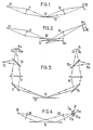
- the means comprise a source 10 of monochromatic light associated with a lens 11 which forms from the source an image 12 which is on the surface of the wafer 13 when the latter is in its nominal position, as indicated in FIG. 1.
- Means of light recovery shown schematically in the form of a lens 14, form of the spot of light on the surface 13 an image which, when the wafer 13 is in its nominal position, is centered relative to a differential photodetector 15, which may in particular be constituted either by a diode with two quadrants, or by two separate diodes. There is thus obtained by difference an error signal which is introduced into a control loop.
- any offset in altitude ⁇ z of the section 13 causes an offset ⁇ x of the image on the differential photodetector 15, therefore an error signal which is an increasing function of ⁇ x and whose sign depends on the direction of ⁇ z.
- Such an autofocus device can be very sensitive, especially if it uses a very oblique angle. But it has a serious drawback.
- An irregularity in the reflection of the surface of the wafer 13 causes an asymmetry in the intensity distribution of the spot and can lead to a focusing error.
- the means of detection of the deviations then comprise a source, for example a laser diode, an optic for focusing the light emitted in the form of a spot, an optic comprising a mirror for picking up the reflected light and returning it along a path opposite to the outward path to a deviation detector.
- the invention aims to provide a projection device of the type defined above, meeting better than those previously known the requirements of practice, in particular in that it comprises an automatic focusing device making it possible to simply spread problems related to image surface reflection defects.
- the invention proposes in particular an apparatus in which two sets of said means are provided, corresponding to reverse paths of the light, and means for summing the differential signals supplied by the two photodetectors.
- the automatic focusing device advantageously further comprises means for detecting angular deviations, that is to say in attitude, between the image surface and a nominal position.
- These means may in particular comprise a source for illuminating the surface by a parallel beam in oblique incidence and means for focusing the image of the source on a four-quadrant photodetector, the grouping of the output signals of the four quadrants allowing to obtain attitude error signals around two perpendicular axes.
- the invention also aims to solve a particular problem in the case of photorepeaters.
- graticule inspection apparatuses are known by photometric comparison of two homologous zones of adjacent patterns. But this solution has many disadvantages. It is indeed the crosshair that we control, and not the image of the crosshair in the plane of the slice. And, in addition, there is a risk of dust being deposited during the transfer between the recording equipment and the photorepeater.
- the invention also aims to eliminate this drawback. To this end, it proposes a projection device constituting a photorepeater, comprising means for forming two homologous zones of adjacent patterns on two photoelectric detectors and for measuring the difference in output signals of the two detectors.
- This solution is applicable whenever several elementary integrated circuit patterns appear on the same reticle, which is frequently the case since this thus reduces the duration of photorepetition on a wafer.
- the actual image is examined directly and not the reticle, which makes it possible to take into account only the defects likely to be actually printed on the silicon wafer and to accept reticles which would be rejected on a conventional inspection device.
- the fault detection resolution is of the same order as the resolution of the objective, that is to say equal to or even less than one micron.
- the various components of the device can occupy very different positions relative to those which are used directly for projection.
- the angular deviation detection means can use a light path making an angle, for example a right angle, with the light paths in said sets of means.
- the first set (in which the elements corresponding to those in FIG. 1 are designated by the same reference number) comprises a monochromatic light source 10 whose output beam is collected by a semi-transparent plate 16 whose role will appear more far.
- the beam reflected by this blade is focused by a lens 11 and a deflection mirror 17 in a spot 12 which is on the surface of the wafer 13 when the latter occupies its nominal position.
- a mirror 17a symmetrical to the mirror 17 and a lens 14 symmetrical to the lens 11 refocus the spot 12 on a differential photodetector 15 through a semi-transparent plate 16a.
- a system comprising the semi-transparent plate 16a, the lens 14 and the mirror 17a forms from the source 10a an image merged with the spot 12.
- the light reflected by the surface 13 is taken up by the mirror 17, the lens 11 and the semi-transparent plate 16 for forming an image on a photodetector 15a similar to the photodetector 15.
- the error signal will be:
- the detectors will obviously be placed and adjusted so that the output signal, which can be produced by a conventional analog adder circuit, is zero when the surface 13 occupies its nominal position.
- the problem encountered in the case of a single passage of light is eliminated: in fact, the image of an asymmetric spot on the photodetector 15 will also be asymmetrical in the same way on the photodetector 15a. Furthermore, the sources 10 and 10a can without drawback have slightly different intensities, because the average of the two photoelectric signals is used.
- photorepeaters generally include an automatic focusing device, but which only ensures the correction of deviations in altitude.
- the present invention makes it possible to easily carry out a control of adjustment in trim, the interest of which has so far not been appreciated.
- an automatic focusing in plate is extremely desirable, because it alone makes it possible to correct slow defects in flatness of the silicon wafers.
- FIGS. 4 and 5 show means for detecting difference in attitude which can be incorporated in a projection apparatus to supply, to a focusing device, the input signals necessary for adjustment in attitude.
- the means shown in FIGS. 4 and 5 comprise means making it possible to send, on edge 13, a monochromatic parallel light beam, in oblique incidence.
- These means comprise a source 18 and an optic shown diagrammatically by a lens 19.
- a second optic also shown diagrammatically by a lens 20, focuses the image of the source point 18 on a quadruple photodetector 21 which can be formed by. a diode with four quadrants D 11 ' D 12 , D 13 and D 14 .
- an offset in attitude ⁇ around an axis perpendicular to the plane of the figure results in an offset ⁇ x on the photodetector 21. If we denote by D 11 , D 12 , D 13 and D 14 the output signals of the four quadrants, the corresponding error signal will be:
- Error signals can be injected into servo loops at ⁇ and ⁇ . These loops will not be described here, any more than the mechanical devices for correct positioning, since they can be of a conventional type, such as for example that described in "The Bell System Technical Journal", November 1970, pp. 2158.2160.
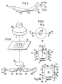
- the means for detecting deviation in altitude and in attitude can be located around the objective of the same photorepeater, as shown in FIGS. 6 and 7; the optical paths of the difference in altitude and attitude measurement means are crossed and the paths frame the objective 22.
- the sources 15, 15a and 18 can be constituted by independent emitters but of sufficient intensity (laser diode for example ) or by the terminal parts of optical fibers.
- the return mirrors 17 and 17a as well as the semi-transparent blades 16 and 16a are formed by prisms.
- FIG. 7A where the members corresponding to those of FIG. 7 are designated by the same reference number, a single source 10 is used for the focus and trim checks.
- the parallel light brush coming from the source 10 is divided by a semi-transparent separating blade 30 into a reflected beam which follows a first path and a transmitted brush whose part reflected by a second separating blade 31 follows a second path, symmetrical with the first when the surface 13 of the silicon wafer has a correct attitude.
- the source points are constituted by respective diaphragms 35 and 35a, the image of which is formed, respectively by the lenses 11 and 11a, on the surface 13.
- the two p hotodetectors 15 and 15a collect the light coming from the wafer 13 and transmitted respectively through the blades 30 and 31.
- the attitude control uses a fraction of the brush which returns to the photodetector 15a, a fraction sampled by reflection on a semi-transparent separating plate 32 and returned to the photodetector 21, generally constituted by a diode with four quadrants. This diode is located at the focal point of the lens 11.
- FIG. 8 schematically shows the reduction objective 22 of the photorepeater which makes it possible to form, from the object reticle 23, once the latter in place in the photorepeater, a real aerial image 24. Inspection and verification are carried out by comparison between the homologous areas of two adjacent patterns, which does not constitute a real limitation, because reasons of speed generally lead to exposing several patterns at the same time. It may be noted in passing that the useful field of a photorepeater is generally of the order of 1 cm ⁇ 1 cm and that the invention will therefore be usable each time the unit dimension of each pattern does not exceed 0.5 cm, which is the most common case.
- the inspection means comprise two mirrors or, as illustrated in FIG. 8, two total reflection prisms 25 and 25a in the form of a half-cube. These two prisms send two homologous images of a small surface of the integrated circuit onto two photosensitive detectors 26 and 26a via two microscope objectives 27 and 27a. All of these elements can constitute a very compact unit, housed near the silicon wafer, on a support secured to the xy table which carries the wafer.
- the signals measured by the photodetectors 26 and 26a are different if the homologous surfaces, delimited by circles in FIG. 8, do not have the same transmission. The difference between the two signals indicates the presence of an opaque or transparent defect in one of the two images.
- each photoelectric detector 26 and 26a will correspond for example to a rectangle of 1 x 5 microns or of 1 x 10 microns. It is thus possible to analyze the image of the reticle by scanning of the television type, by successive lines, 5 microns or 10 microns wide. The complete comparison operation between two circuits of 5 x 5 mm therefore leads to scanning 1000 lines of width 5 microns and length 5 mm, ie a total travel of the table of 5 m. The total control time will therefore only be 100 seconds if the movement is made at an average speed of 5 cm / s. We see that we do not significantly reduce the speed of the photorepeater due to the inspection of the reticle before exposing one or more batches of slices.
- the means shown in FIG. 8 can be saved with their position in memory of a minicomputer which, at the end of the check, provides the map of the circuit. This image of the circuit helps to find the fault under a microscope and to make it disappear, if possible, for example if it is a dust. It is not necessary to describe here the means of recording in memory, since they can be conventional.
Landscapes
- Physics & Mathematics (AREA)
- General Physics & Mathematics (AREA)
- Optics & Photonics (AREA)
- Exposure Of Semiconductors, Excluding Electron Or Ion Beam Exposure (AREA)
- Exposure And Positioning Against Photoresist Photosensitive Materials (AREA)
- Variable Magnification In Projection-Type Copying Machines (AREA)
- Automatic Focus Adjustment (AREA)
- Focusing (AREA)
- Investigating Materials By The Use Of Optical Means Adapted For Particular Applications (AREA)
- Testing Or Measuring Of Semiconductors Or The Like (AREA)
Claims (6)
Applications Claiming Priority (2)
| Application Number | Priority Date | Filing Date | Title |
|---|---|---|---|
| FR8107709 | 1981-04-16 | ||
| FR8107709A FR2504281A1 (fr) | 1981-04-16 | 1981-04-16 | Appareil de projection a dispositif de mise au point |
Publications (2)
| Publication Number | Publication Date |
|---|---|
| EP0063980A1 EP0063980A1 (de) | 1982-11-03 |
| EP0063980B1 true EP0063980B1 (de) | 1985-06-26 |
Family
ID=9257505
Family Applications (1)
| Application Number | Title | Priority Date | Filing Date |
|---|---|---|---|
| EP82400636A Expired EP0063980B1 (de) | 1981-04-16 | 1982-04-06 | Projektionsapparat mit einer Anordnung zum Scharfeinstellen |
Country Status (5)
| Country | Link |
|---|---|
| US (1) | US4477185A (de) |
| EP (1) | EP0063980B1 (de) |
| JP (1) | JPS57188027A (de) |
| DE (1) | DE3264399D1 (de) |
| FR (1) | FR2504281A1 (de) |
Families Citing this family (25)
| Publication number | Priority date | Publication date | Assignee | Title |
|---|---|---|---|---|
| JPS58113706A (ja) * | 1981-12-26 | 1983-07-06 | Nippon Kogaku Kk <Nikon> | 水平位置検出装置 |
| JPS59121932A (ja) * | 1982-12-28 | 1984-07-14 | Fujitsu Ltd | 自動焦点制御装置 |
| US4845373A (en) * | 1984-02-22 | 1989-07-04 | Kla Instruments Corporation | Automatic alignment apparatus having low and high resolution optics for coarse and fine adjusting |
| NL8401710A (nl) * | 1984-05-29 | 1985-12-16 | Philips Nv | Inrichting voor het afbeelden van een maskerpatroon op een substraat. |
| FR2580087B1 (de) * | 1985-04-03 | 1988-12-02 | Hispano Suiza Sa | |
| US4810077A (en) * | 1986-02-13 | 1989-03-07 | Spectra-Tech, Inc. | Grazing angle microscope |
| US4721386A (en) * | 1986-07-18 | 1988-01-26 | Barnes Engineering Company | Three-axis angular monitoring system |
| US4821196A (en) * | 1987-02-20 | 1989-04-11 | International Business Machines Corporation | High resolution automatic focus correction electronic subsystem for E-beam lithography |
| US4886958A (en) * | 1988-03-25 | 1989-12-12 | Texas Instruments Incorporated | Autofocus system for scanning laser inspector or writer |
| DE3921661C1 (de) * | 1989-06-30 | 1991-01-17 | Fraunhofer-Gesellschaft Zur Foerderung Der Angewandten Forschung Ev, 8000 Muenchen, De | |
| FR2674036B1 (fr) * | 1991-03-13 | 1993-07-30 | Mrejen Jean Jacques | Procede de commande de mise au point pour la prise de vue et organe de commande a cette fin. |
| EP0505717B1 (de) * | 1991-03-25 | 1998-07-29 | Heidelberger Druckmaschinen Aktiengesellschaft | Verfahren und Vorrichtung zur optischen Messung von Distanzen |
| JP2943499B2 (ja) * | 1992-04-22 | 1999-08-30 | 日本電気株式会社 | 高さ測定方法および装置 |
| US5311288A (en) * | 1992-07-06 | 1994-05-10 | Opal Technologies Ltd. | Method and apparatus for detecting surface deviations from a reference plane |
| US5510892A (en) * | 1992-11-25 | 1996-04-23 | Nikon Corporation | Inclination detecting apparatus and method |
| US5636013A (en) * | 1995-01-04 | 1997-06-03 | Hutchinson Technology Incorporated | Suspension assembly static attitude and distance measuring instrument |
| US6166808A (en) * | 1996-12-24 | 2000-12-26 | U.S. Philips Corporation | Optical height meter, surface-inspection device provided with such a height meter, and lithographic apparatus provided with the inspection device |
| US5844727A (en) * | 1997-09-02 | 1998-12-01 | Cymer, Inc. | Illumination design for scanning microlithography systems |
| US6774945B1 (en) | 1999-10-18 | 2004-08-10 | Hewlett-Packard Development Company, L.P. | Focusing apparatus for image recording system |
| DE10026830A1 (de) * | 2000-05-30 | 2001-12-06 | Zeiss Carl Jena Gmbh | Optischer Sensor zur Messung des Abstands und/oder der Neigung einer Fläche |
| DE10233087A1 (de) * | 2002-07-19 | 2004-02-05 | Roche Diagnostics Gmbh | Reflexionsphotometrisches Analysesystem |
| ES2617664T3 (es) | 2009-03-11 | 2017-06-19 | Sakura Finetek U.S.A., Inc. | Procedimiento de enfoque automático y dispositivo de enfoque automático |
| DE102013103971A1 (de) | 2013-04-19 | 2014-11-06 | Sensovation Ag | Verfahren zum Erzeugen eines aus mehreren Teilbildern zusammengesetzten Gesamtbilds eines Objekts |
| US10007102B2 (en) | 2013-12-23 | 2018-06-26 | Sakura Finetek U.S.A., Inc. | Microscope with slide clamping assembly |
| US11280803B2 (en) | 2016-11-22 | 2022-03-22 | Sakura Finetek U.S.A., Inc. | Slide management system |
Family Cites Families (14)
| Publication number | Priority date | Publication date | Assignee | Title |
|---|---|---|---|---|
| US3517992A (en) * | 1968-04-24 | 1970-06-30 | Leitz Ernst Gmbh | Automatic focusing slide projector |
| US3612698A (en) * | 1969-05-01 | 1971-10-12 | Ibm | Automatic holographic wafer positioning system and method |
| GB1312663A (en) * | 1970-05-28 | 1973-04-04 | Ti Group Services Ltd | Optical control means |
| US3645623A (en) * | 1970-09-25 | 1972-02-29 | Raymond A Patten | Apparatus for monitoring film thickness by reflecting a light beam from the film surface |
| DE2225972A1 (de) * | 1972-05-27 | 1973-12-13 | Agfa Gevaert Ag | Automatische fokussiervorrichtung |
| US3865483A (en) * | 1974-03-21 | 1975-02-11 | Ibm | Alignment illumination system |
| DE2539206A1 (de) * | 1975-09-03 | 1977-03-17 | Siemens Ag | Verfahren zur automatischen justierung von halbleiterscheiben |
| JPS5245907A (en) * | 1975-10-09 | 1977-04-12 | Agency Of Ind Science & Technol | Automatic optical path adjusting device |
| JPS53123103A (en) * | 1977-04-02 | 1978-10-27 | Mansei Kogyo Kk | Optical information reader |
| JPS54133305A (en) * | 1978-04-07 | 1979-10-17 | Hitachi Ltd | Information recorder |
| JPS5545122A (en) * | 1978-09-25 | 1980-03-29 | Mansei Kogyo Kk | Focus controller of optical reader |
| FR2445512A1 (en) * | 1978-12-27 | 1980-07-25 | Thomson Csf | Position detecting system for image forming appts. - includes two part photodiode providing two signals with difference proportional to position error |
| NL186353C (nl) * | 1979-06-12 | 1990-11-01 | Philips Nv | Inrichting voor het afbeelden van een maskerpatroon op een substraat voorzien van een opto-elektronisch detektiestelsel voor het bepalen van een afwijking tussen het beeldvlak van een projektielenzenstelsel en het substraatvlak. |
| JPS5696203A (en) * | 1979-12-27 | 1981-08-04 | Fujitsu Ltd | Detection device for optical position |
-
1981
- 1981-04-16 FR FR8107709A patent/FR2504281A1/fr active Granted
-
1982
- 1982-04-06 DE DE8282400636T patent/DE3264399D1/de not_active Expired
- 1982-04-06 EP EP82400636A patent/EP0063980B1/de not_active Expired
- 1982-04-16 US US06/369,117 patent/US4477185A/en not_active Expired - Fee Related
- 1982-04-16 JP JP57062604A patent/JPS57188027A/ja active Pending
Non-Patent Citations (1)
| Title |
|---|
| SOLID STATE TECHNOLOGY, vol.23, no.6, juin 1980, Port Washington, N.Y. (US), S. WITTEKOEK: "Step-and-repeat wafer imaging", pages 80-84 * |
Also Published As
| Publication number | Publication date |
|---|---|
| JPS57188027A (en) | 1982-11-18 |
| FR2504281A1 (fr) | 1982-10-22 |
| FR2504281B1 (de) | 1985-04-12 |
| EP0063980A1 (de) | 1982-11-03 |
| US4477185A (en) | 1984-10-16 |
| DE3264399D1 (en) | 1985-08-01 |
Similar Documents
| Publication | Publication Date | Title |
|---|---|---|
| EP0063980B1 (de) | Projektionsapparat mit einer Anordnung zum Scharfeinstellen | |
| EP0015173B1 (de) | Optisches Ausrichtsystem für zwei Patronen und Photorepetierer mit solchem System | |
| JP4256137B2 (ja) | デュアル・ビーム対称高さシステムおよび方法 | |
| JP5773939B2 (ja) | 欠陥検査装置および欠陥検査方法 | |
| US9915622B2 (en) | Wafer inspection | |
| EP0159210B1 (de) | Optische Vorrichtung zum Messen der Annäherung an einer Fläche und Verfahren zum Wiedergewinnen des Profils einer solchen Fläche | |
| EP0401351B1 (de) | Verfahren und vorrichtung für optische messungen | |
| FR2538923A1 (fr) | Procede et dispositif d'alignement optique de motifs dans deux plans rapproches dans un appareil d'exposition comprenant une source de rayonnement divergent | |
| JP2010112803A (ja) | 基板検査装置及び光検出装置 | |
| KR102687194B1 (ko) | 표면 변형들의 이미지 기반 계측 | |
| FR2504288A1 (fr) | Procede et appareil d'alignement d'une tranche de semi-conducteur | |
| EP0015789A1 (de) | Optische photorepetierende Projektionsvorrichtung | |
| CN115427754B (zh) | 高灵敏度的基于影像的反射测量 | |
| EP0156683B1 (de) | Gerät für optische Microlithografie mit lokalem Ausrichtungssystem | |
| EP0402191B1 (de) | Verfahren und Vorrichtung zum Messen der Linienbreite mit optischem Abtasten | |
| FR2707018A1 (de) | ||
| WO2006097645A2 (fr) | Dispositif de mesure optique par triangulation optique | |
| WO2021199340A1 (ja) | 欠陥検査装置及び欠陥検査方法 | |
| JP2506725B2 (ja) | パタ−ン欠陥検査装置 | |
| EP0088691B1 (de) | Justiereinrichtung bei Maschinen zum Herstellen integrierter Schaltungen | |
| WO2010034955A1 (fr) | Mise au point d'un microscope a reflexion | |
| FR2684202A1 (fr) | Procede et dispositif holographiques perfectionnes en lumiere incoherente. | |
| FR2518255A1 (fr) | Appareil d'alignement precis de plaquettes semi-conductrices | |
| EP0083268B1 (de) | Verfahren zur automatischen Regelung der Schärfe von auf einen Schirm projizierten Bildern und Geräte dazu | |
| JPH10122831A (ja) | 表面検査装置 |
Legal Events
| Date | Code | Title | Description |
|---|---|---|---|
| PUAI | Public reference made under article 153(3) epc to a published international application that has entered the european phase |
Free format text: ORIGINAL CODE: 0009012 |
|
| AK | Designated contracting states |
Designated state(s): CH DE GB IT NL |
|
| 17P | Request for examination filed |
Effective date: 19821129 |
|
| ITF | It: translation for a ep patent filed | ||
| RAP1 | Party data changed (applicant data changed or rights of an application transferred) |
Owner name: MATRA GCA S.A. |
|
| GRAA | (expected) grant |
Free format text: ORIGINAL CODE: 0009210 |
|
| AK | Designated contracting states |
Designated state(s): CH DE GB IT LI NL |
|
| REF | Corresponds to: |
Ref document number: 3264399 Country of ref document: DE Date of ref document: 19850801 |
|
| PLBE | No opposition filed within time limit |
Free format text: ORIGINAL CODE: 0009261 |
|
| STAA | Information on the status of an ep patent application or granted ep patent |
Free format text: STATUS: NO OPPOSITION FILED WITHIN TIME LIMIT |
|
| 26N | No opposition filed | ||
| PGFP | Annual fee paid to national office [announced via postgrant information from national office to epo] |
Ref country code: NL Payment date: 19870430 Year of fee payment: 6 |
|
| PG25 | Lapsed in a contracting state [announced via postgrant information from national office to epo] |
Ref country code: LI Effective date: 19880430 Ref country code: CH Effective date: 19880430 |
|
| PG25 | Lapsed in a contracting state [announced via postgrant information from national office to epo] |
Ref country code: NL Effective date: 19881101 |
|
| PG25 | Lapsed in a contracting state [announced via postgrant information from national office to epo] |
Ref country code: GB Effective date: 19881121 |
|
| NLV4 | Nl: lapsed or anulled due to non-payment of the annual fee | ||
| GBPC | Gb: european patent ceased through non-payment of renewal fee | ||
| REG | Reference to a national code |
Ref country code: CH Ref legal event code: PL |
|
| PG25 | Lapsed in a contracting state [announced via postgrant information from national office to epo] |
Ref country code: DE Effective date: 19890103 |