EP0064081B1 - Detecteur d'image a circuit ouvert d'un dispositif de couplage de charge - Google Patents
Detecteur d'image a circuit ouvert d'un dispositif de couplage de charge Download PDFInfo
- Publication number
- EP0064081B1 EP0064081B1 EP81903177A EP81903177A EP0064081B1 EP 0064081 B1 EP0064081 B1 EP 0064081B1 EP 81903177 A EP81903177 A EP 81903177A EP 81903177 A EP81903177 A EP 81903177A EP 0064081 B1 EP0064081 B1 EP 0064081B1
- Authority
- EP
- European Patent Office
- Prior art keywords
- charge
- capacitor
- open circuit
- diode
- ccd
- Prior art date
- Legal status (The legal status is an assumption and is not a legal conclusion. Google has not performed a legal analysis and makes no representation as to the accuracy of the status listed.)
- Expired
Links
- 230000005855 radiation Effects 0.000 claims abstract description 61
- 230000004907 flux Effects 0.000 claims abstract description 51
- 230000008859 change Effects 0.000 claims abstract description 10
- 230000010354 integration Effects 0.000 claims description 19
- 238000002347 injection Methods 0.000 claims description 16
- 239000007924 injection Substances 0.000 claims description 16
- 239000004065 semiconductor Substances 0.000 claims description 11
- 239000004020 conductor Substances 0.000 claims 1
- 239000003990 capacitor Substances 0.000 abstract description 65
- 230000004044 response Effects 0.000 abstract description 5
- 238000010586 diagram Methods 0.000 description 16
- 238000009792 diffusion process Methods 0.000 description 15
- 230000007423 decrease Effects 0.000 description 11
- 230000004888 barrier function Effects 0.000 description 7
- 239000000758 substrate Substances 0.000 description 6
- 230000008878 coupling Effects 0.000 description 3
- 238000010168 coupling process Methods 0.000 description 3
- 238000005859 coupling reaction Methods 0.000 description 3
- 230000003247 decreasing effect Effects 0.000 description 3
- 238000005070 sampling Methods 0.000 description 3
- VYPSYNLAJGMNEJ-UHFFFAOYSA-N Silicium dioxide Chemical compound O=[Si]=O VYPSYNLAJGMNEJ-UHFFFAOYSA-N 0.000 description 2
- 230000008901 benefit Effects 0.000 description 2
- 230000000694 effects Effects 0.000 description 2
- 230000005684 electric field Effects 0.000 description 2
- 239000011521 glass Substances 0.000 description 2
- NPXOKRUENSOPAO-UHFFFAOYSA-N Raney nickel Chemical compound [Al].[Ni] NPXOKRUENSOPAO-UHFFFAOYSA-N 0.000 description 1
- 239000002800 charge carrier Substances 0.000 description 1
- 230000007547 defect Effects 0.000 description 1
- 230000005669 field effect Effects 0.000 description 1
- 238000001914 filtration Methods 0.000 description 1
- 229910052738 indium Inorganic materials 0.000 description 1
- APFVFJFRJDLVQX-UHFFFAOYSA-N indium atom Chemical compound [In] APFVFJFRJDLVQX-UHFFFAOYSA-N 0.000 description 1
- 238000005468 ion implantation Methods 0.000 description 1
- 238000012886 linear function Methods 0.000 description 1
- 229910044991 metal oxide Inorganic materials 0.000 description 1
- 150000004706 metal oxides Chemical class 0.000 description 1
- 238000000034 method Methods 0.000 description 1
- 230000009467 reduction Effects 0.000 description 1
- 229920006395 saturated elastomer Polymers 0.000 description 1
- 235000012239 silicon dioxide Nutrition 0.000 description 1
- 239000000377 silicon dioxide Substances 0.000 description 1
Images


Classifications
-
- H—ELECTRICITY
- H10—SEMICONDUCTOR DEVICES; ELECTRIC SOLID-STATE DEVICES NOT OTHERWISE PROVIDED FOR
- H10F—INORGANIC SEMICONDUCTOR DEVICES SENSITIVE TO INFRARED RADIATION, LIGHT, ELECTROMAGNETIC RADIATION OF SHORTER WAVELENGTH OR CORPUSCULAR RADIATION
- H10F39/00—Integrated devices, or assemblies of multiple devices, comprising at least one element covered by group H10F30/00, e.g. radiation detectors comprising photodiode arrays
- H10F39/10—Integrated devices
- H10F39/12—Image sensors
- H10F39/15—Charge-coupled device [CCD] image sensors
- H10F39/157—CCD or CID infrared image sensors
- H10F39/1575—CCD or CID infrared image sensors of the hybrid type
-
- H—ELECTRICITY
- H04—ELECTRIC COMMUNICATION TECHNIQUE
- H04N—PICTORIAL COMMUNICATION, e.g. TELEVISION
- H04N25/00—Circuitry of solid-state image sensors [SSIS]; Control thereof
- H04N25/70—SSIS architectures; Circuits associated therewith
- H04N25/76—Addressed sensors, e.g. MOS or CMOS sensors
- H04N25/77—Pixel circuitry, e.g. memories, A/D converters, pixel amplifiers, shared circuits or shared components
-
- H—ELECTRICITY
- H10—SEMICONDUCTOR DEVICES; ELECTRIC SOLID-STATE DEVICES NOT OTHERWISE PROVIDED FOR
- H10D—INORGANIC ELECTRIC SEMICONDUCTOR DEVICES
- H10D44/00—Charge transfer devices
- H10D44/40—Charge-coupled devices [CCD]
- H10D44/45—Charge-coupled devices [CCD] having field effect produced by insulated gate electrodes
- H10D44/452—Input structures
Definitions
- the invention relates to a charge transfer device imager comprising: a photosensitive semiconductor diode comprising first and second regions of opposite conductivity types disposed to receive an incident flux of radiation, at least one of said regions being unconnected so that said diode has an open circuit junction voltage proportional to said radiation flux, a capacitive electrode overlying said one unconnected region, a charge transfer device, and connecting means for connecting said charge transfer device to said capacitive electrode.
- Such a charge transfer device imager is disclosed in US-A-3 808 435.
- the means for connecting the charge transfer device to the capacitive electrode is comprised of a transfer gate which is controlled either by a clock signal or by the output voltage of said capacitive electrode.
- a reference potential has to be established at the capacitive electrode by means of a further gate or a resistor connected to a reference voltage.
- the known imager requires the incidence of a chopped radiation, either by means of a shutter or of a scanning device.
- this charge transfer device imager cannot be used in focal plane array imagers which are neither combined with scanning means nor with shutter means.
- the connecting means is comprised of a direct injection channel including means for removing a charge packet from the charge transfer device and storing it on said capacitive electrode to begin an integration period, and means for retrieving at least a portion of said charge packet from said capacitive electrode to terminate said integration period and for returning at least said portion to said charge transfer device, wherein the difference between the charge removed from the charge transfer device and the charge returned to the charge transfer device by said removing and returning means is proportional to the change in said radiation flux during said integration period.
- a charge transfer device imager comprises an open voltage photodiode including a capacitor plate formed monolithically with a P-N junction diode.
- the capacitor plate together with one side of the P-N junction, forms a capacitor which is charged by the photocurrent of the diode.
- the voltage across the capacitor controls the output current of a charge coupled device (CCD) register.
- CCD charge coupled device
- the photodetector diode of the present invention operates in an open circuit configuration so that no net current flows across the diode junction as long as the flux of incident radiation is constant. Initially, radiation incident upon the diode does generate a current flow across the diode junction which charges the capacitor to an open circuit voltage proportional to the flux of the incident radiation.
- the open circuit photodiode capacitor of this invention controls the current in a CCD register by accepting a charge packet of predetermined size from the CCD register, the charge packet being stored on the photodiode capacitor during an integration period when radiation is incident on the photodiode. At the end of the integration period, a charge packet of different size is returned to the CCD register.
- the change in the size of the charge packet is proportional to the change in radiation flux during the integration period and therefore is representative of a video signal generated by the photodiode.
- the advantage of this direct injection device is that it is inherently insensitive to background radiation or radiation having a constant flux.
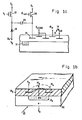
- prior art infrared imagers typically include a photosensitive diode 10 which generates a photocurrent creating a voltage drop across a resistive load device such as a metal oxide semiconductor field effect transistor (MOSFET) 12, the voltage drop determining the voltage on a control gate 14 which regulates the injection of charge from an input diffusion 16 into a CCD register 18.
- a resistive load device such as a metal oxide semiconductor field effect transistor (MOSFET) 12
- MOSFET metal oxide semiconductor field effect transistor
- 1b is a simplified perspective view of the prior art photodiode 10 which includes a diffusion 10a of P-type conductivity in the top surface of a semiconductive layer 20 of N-type conductivity, an electrical contact 10b to the P-type diffusion 10a and a bias electrode 10c insulated by a dielectric layer 10d.
- an external coupling capacitor 24 must be interposed between the photodiode output 10b and the CCD control gate 14 in order to filter out the constant DC output generated by background radiation in order to prevent saturation of the detector by excessive background radiation or a reduction in dynamic range of the detector.
- the radiation 22 incident on the photodiode 10 includes both an image from which a video signal is to be generated and background radiation which contains no information. It is desirable to create a video signal from an image in the presence of either a light or a dark background, which can only be accomplished within the limited dynamic range of the CCD register 18 by filtering out background radiation from the video signal.
- the background radiation typically has a constant flux which generates a constant or a DC component in the output photocurrent of the photodiode 10.
- the potential on one plate of the external capacitor 24 is reset to a voltage V r at the end of each CCD clock period under the control of a reset switch 26 gated by a clock signal ⁇ rst .
- a significant disadvantage of this arrangement is that the capacitor 24 takes up a significant amount of space, thus reducing the device density on the semiconductor layer 20.
- the bias electrode 10c overlies the junction between the diode diffusion 10a and the semiconductor layer 20 and has an applied voltage V h which depletes surface charge carriers from the-region of the diode junction to prevent leakage across the junction.
- the load MOSFET 12, the coupling capacitor 24 and the bias electrode 10c take up significant amounts of space on the underlying semiconductor layer, thus limiting the density of the device.
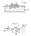
- the invention makes use of an open circuit photodiode 30 comprising a semiconductive layer 20 of N-type conductivity, a diode diffusion 30a of P-type conductivity in the semiconductor layer 20 and an insulated capacitor plate 32 overlying the semiconductor layer 20 in registration with the diode diffusion 30a so as to form a photodiode capacitor 37.
- the diode diffusion 30a is not electrically connected so that the didoe 30 is in an open circuit configuration.
- Radiation 22 incident upon the diode 30 generates current flow across diode junction 36 between the the diffusion 30a and the remainder of the semiconductor layer 20.
- the current flow across the junction 36 charges the junction 36 and the capacitor 37 to an open circuit voltage which is proportional to the incident radiation flux.
- the open circuit photodiode 30 is formed on a semiconductive substrate or layer 20 of N-type conductivity, and the P-type diode region 30a may be formed by ion implantation or diffusion.
- a dielectric layer 38 such as silicon dioxide is placed over the top surface of the substrate 20 and an aluminum-nickel capacitor plate 32 is placed over the dielectric layer in registration with the diode region 30a.
- a glass layer 40 is placed over the capacitor plate 32 and over exposed portions of the dielectric layer 38, the glass layer 40 having a contact opening 42 to the capacitor plate 32 in which an indium bump 44 is deposited as an electrode contact to the capacitor plate 32.
- a bias voltage V b is applied to the substrate 20 of Fig. 2 and is preferably selected so as to impose an ' electrical field which is equal and opposite to the electrical field created by surface charge Q ss at the surface of the substrate 20.
- the structure of the open circuit diode capacitor 37 described above is used in a novel open circuit direct injection device useful in charge coupled device imagers.
- This device is illustrated for the sake of simplified explanation as a bucket brigade device in Fig. 3 and includes an intervening bucket brigade direct injection channel 70 interposed between the open circuit photodiode capacitor 37 and a charge coupled device serial output register 72.
- the direct injection channel 70 includes a first transfer MOSFET 74, a MOS store capacitor 76 and an input MOSFET 78 connected to the capacitor plate 32 of the open circuit photodiode capacitor 37.
- the direct injection device of Fig. 3 actually injects the charge stored on the open circuit photodiode capacitor 37 directly into the output CCD register
- a charge packet of a predetermined size Q fz is diverted from the CCD register 72 and stored on the capacitor plate 32 during an integration period.
- the charge packet is then retrieved from the open circuit photodiode capacitor plate 32 and reinjected into the CCD register 72.
- the size of the charge packet is "altered" during the integration period if the radiation flux incident upon the open circuit photodiode 30 has changed.
- the change in the size of the charge packet represents the video signal of the image viewed by the photodiode 30.
- Operation of the open circuit direct injection device of Fig. 3 begins when a charge packet of predetermined size, preferably of a size equal to the fat zero level Qfz of the CCD register 72, is transferred serially in the CCD register 72.
- a clock signal ⁇ ' tr turns on to apply an attractive voltage to the gate of the MOSFET 74 while a clock signal ⁇ ' store turns on to apply an attractive voltage to the plate of the MOS capacitor 76 so that the charge packet is transferred out of the CCD register 72 beneath the gate 74a of the transfer MOSFET 74 and stored on the store capacitor 76.
- the clock signals ⁇ ' tr and ⁇ ' store turn off while the clock signal ⁇ ' in applied to the gate of the input MOSFET 78 is on so that the charge packet is withdrawn from the capacitor 76 and flows through the input MOSFET 78 to be stored on the detector capacitor plate 32, after which the clock signal ⁇ ' in turns off.
- the open circuit voltage V oc on the capacitor plate 32 changes by a proportional amount ⁇ V oc' in accordance with the discussion given above in connection with Fig. 3.
- the clock signals ⁇ '," and ( ⁇ ' Store turn on so that the charge packet is retrieved from the capacitor plate 32 to again be stored on the MOS capacitor 76, after which the clock signal ⁇ ," turns off.
- the open circuit voltage on the capacitor plate 32 has changed, the amount of charge released from the capacitor plate 32 to the store capacitor 76 is not equal to the original size Qfz of the charge packet prevrously withdrawn from the CCD register 72. It may be shown that the change AQ in the size of the charge packet from its original fat zero level Q fz is equal to the capacitance C det of the detector capacitor 37 multiplied by the change ⁇ V oc in the open circuit voltage V oc of the photodiode 30, which may be expressed as follows:
- AQ may be positive or negative, depending upon whether the radiation flux increased or decreased during the integration period.
- the size Q of the charge packet stored on the store capacitor 76 at the end of the integration period is equal to the fat zero level Q fz of the CCD register 72 plus AQ which may be expressed as follows:
- the charge packet stored on the store capacitor 76 is reinjected into the CCD register 72 when the clock signal ⁇ ' store turns off while the clock signal ⁇ 'tr turns on so that the charge packet is withdrawn from the store capacitor 76 and passes beneath the transfer gate 74a and into the CCD register 72.
- a serial train of charge packets may be generated in the output register 72 forming a video signal represented by the difference AQ between the size of each charge packet and the fat zero level Q fz .
- Fig. 4a The preferred embodiment of the invention is illustrated in Fig. 4a in which the open circuit photodiode capacitor 37 controls the direct injection of charge packets transferred serially in the CCD output register 72 by means of an intervening CCD channel 70' formed with the output CCD register 72 on an N-type semiconductive layer 80 including a CCD electrode 72a connected to receive the clock signal ⁇ 'ccd.
- the intervening CCD channel 70' includes a transfer gate 82 connected to receive the clock signal ⁇ ' tr, a store gate 84 connected to receive the clock signal ⁇ ' storen a screen gate 86 connected to a voltage source V scr and an input gate 88 connected to recieve the clock signal ⁇ ' in .
- a P-type diffusion 89 adjacent the input gate 88 is connected to the capacitor plate 32 to permit charge transfer between the capacitor plate 32 and the intermediate CCD channel 70'. It will be easily recognized by those skilled in the art that the intervening CCD channel 70' of Fig. 4a is equivalent to the bucket brigade device 70 of Fig. 3.
- Figs. 6a through 6e are plotted on a time scale expanded from that of Fig. 7a and correspond to the time window between To and Tp of Fig. 7a.
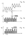
- the total incident radiation flux follows the waveform illustrated in Fig. 7a, in which the sawtooth waveform of the image radiation flux R image illustrated in Fig. 5a is superimposed upon the step function waveform of the background radiation flux R dc illustrated in Fig. 5b. It will be seen that the effects of the background radiation flux R dc are virtually eliminated in the CCD output current I ccd in the device of Fig. 4a.
- operation begins attimeT 10 when the clock signal ⁇ ' ccd turns on, causing the surface potential S 2 of the substrate 80 illustrated in Fig. 4b to fall from the barrier level 91 underlying the CCD electrode 72a to the well level 90, which permits a fat zero charge packet Q fz to be transferred and held beneath the CCD electrode 72a.
- the clock signals ⁇ ' tr and ⁇ ' store illustrated in Figs. 6b and 6c respectively turn on, causing the surface potential S 2 to decrease from the barrier levels 92 and 95 underlying the transfer gate 82 and the store gate 84 respectively, to the well levels 93 and 94 respectively.
- the amount of charge Q, stored in the region 89, 96, 97 immediately increases from an initial level Q o to a new level Q fz +Q 0 as illustrated in Fig. 6e.
- the decreasing radiation flux R illustrated in Fig. 6d causes the open circuit voltage V oc of the photodiode 30 to decrease, reducing the positive charge stored in the P-type diffusion 30a of the open circuit photodiode 30, . causing a corresponding decrease in the negative charge (electrons) stored on the capacitor plate 32.
- Fig. 6e illustrates that, beginning at time T, 3 , the stored charge Q i decreases in proportion to the decrease in radiation flux R illustrated in Fig. 6d.
- the stored charge Q i is removed from the region 89, 96, 97 when the clock signal ⁇ ' store turns on to decrease the surface potential S 2 from the barrier level 95 to the well level 94 so that the stored charge Q, is withdrawn from the region 89, 96, 97 and held beneath the store gate 84.
- the clock signals ⁇ ' ccd and cp' tr turn on to decrease the surface potential S 2 from the barrier levels 92, 91 respectively to the potential- well levels 93, 90 respectively.
- the clock signal ⁇ ' store turns off, causing the surface potential S 2 to increase from the potential well level 94 to the barrier level 95 while at time T 17 the clock signal ⁇ tr is turned off to cause the surface potential S 2 to increase from the potential well level 93 to the barrier level 92, thus causing the stored charge Q i to be injected into the potential well 90' beneath the CCD gate 72a.
- the amount of charge Q ccd injected into the CCD output register 72 at time T 17 is indicated in dashed line in Fig. 10e and is equal to the charge Q, previously stored in the region 89, 96, 97 at time T 14 .
- Figs. 7a-c when the background radiation flux R dc suddenly increases in accordance with its step function waveform as illustrated in Fig. 7a.
- the temporary saturation of the output device is limited to the single integration period beginning at time T a , and Fig. 7c clearly shows that the output current I ccd resumes its usually nearly sawtooth waveform shortly after time T s .
- the output current I ccd is a reliable representation of the image radiation flux R image and is virtually independent of the background radiation flux R dc .
- Truncation of the sawtooth waveform in Fig. 7c occurs in this tutorial example only because the center frequency of the input signal R image of Fig.
- FIG. 7a is close to the sampling frequency defined by the clock signal ⁇ 'store of Fig. 7c. It should be understood that a skilled worker may select a sufficiently high frequency for each clock signal illustrated in Figs. 7a, 7b and 7c so that the sampling frequency of the device of Fig. 4a is significantly greater than the frequency of the image viewed by the device.
- An output video signal may be derived from a plurality of intervening CCD channels 70' and open circuit photodiode capacitors 37 in a planar array (not shown) comprising a plurality of such photodiode capacitors.
- a significant advantage of the open circuit direct injection device of Figs. 3 and 4a is that the video signal (represented by the charge difference ⁇ Q) is virtually insensitive to background radiation having a constant flux.
Landscapes
- Engineering & Computer Science (AREA)
- Multimedia (AREA)
- Signal Processing (AREA)
- Solid State Image Pick-Up Elements (AREA)
- Transforming Light Signals Into Electric Signals (AREA)
Claims (2)
caractérisé en ce que:
Applications Claiming Priority (2)
| Application Number | Priority Date | Filing Date | Title |
|---|---|---|---|
| US20554480A | 1980-11-10 | 1980-11-10 | |
| US205544 | 1980-11-10 |
Publications (3)
| Publication Number | Publication Date |
|---|---|
| EP0064081A1 EP0064081A1 (fr) | 1982-11-10 |
| EP0064081A4 EP0064081A4 (fr) | 1984-04-04 |
| EP0064081B1 true EP0064081B1 (fr) | 1986-08-06 |
Family
ID=22762644
Family Applications (1)
| Application Number | Title | Priority Date | Filing Date |
|---|---|---|---|
| EP81903177A Expired EP0064081B1 (fr) | 1980-11-10 | 1981-11-09 | Detecteur d'image a circuit ouvert d'un dispositif de couplage de charge |
Country Status (5)
| Country | Link |
|---|---|
| EP (1) | EP0064081B1 (fr) |
| JP (1) | JPS57501904A (fr) |
| IL (1) | IL64042A (fr) |
| IT (1) | IT1144513B (fr) |
| WO (1) | WO1982001789A1 (fr) |
Families Citing this family (1)
| Publication number | Priority date | Publication date | Assignee | Title |
|---|---|---|---|---|
| IL72696A (en) * | 1983-08-31 | 1987-12-20 | Texas Instruments Inc | Infrared imaging circuit with sampling and averaging means |
Family Cites Families (5)
| Publication number | Priority date | Publication date | Assignee | Title |
|---|---|---|---|---|
| US3808435A (en) * | 1973-05-29 | 1974-04-30 | Texas Instruments Inc | Infra-red quantum differential detector system |
| US3944849A (en) * | 1974-06-26 | 1976-03-16 | Texas Instruments Inc. | Charge transfer device signal processing |
| JPS5323224A (en) * | 1976-08-16 | 1978-03-03 | Hitachi Ltd | Solid pickup unit |
| US4197469A (en) * | 1978-05-25 | 1980-04-08 | Rockwell International Corporation | Capacitively coupled array of photodetectors |
| US4169273A (en) * | 1978-06-26 | 1979-09-25 | Honeywell Inc. | Photodetector signal processing |
-
1981
- 1981-10-12 IL IL64042A patent/IL64042A/xx unknown
- 1981-11-06 IT IT49650/81A patent/IT1144513B/it active
- 1981-11-09 JP JP56503725A patent/JPS57501904A/ja active Pending
- 1981-11-09 WO PCT/US1981/001497 patent/WO1982001789A1/fr not_active Ceased
- 1981-11-09 EP EP81903177A patent/EP0064081B1/fr not_active Expired
Also Published As
| Publication number | Publication date |
|---|---|
| EP0064081A4 (fr) | 1984-04-04 |
| IL64042A0 (en) | 1982-01-31 |
| IL64042A (en) | 1984-08-31 |
| JPS57501904A (fr) | 1982-10-21 |
| EP0064081A1 (fr) | 1982-11-10 |
| IT1144513B (it) | 1986-10-29 |
| WO1982001789A1 (fr) | 1982-05-27 |
| IT8149650A0 (it) | 1981-11-06 |
Similar Documents
| Publication | Publication Date | Title |
|---|---|---|
| US3969634A (en) | Bucket background subtraction circuit for charge-coupled devices | |
| EP0222624B1 (fr) | Dispositif et procédé pour la conversion photoélectrique de lumière en signaux électriques | |
| EP0511644B1 (fr) | Dispositif état solide de prise de vues | |
| US4338514A (en) | Apparatus for controlling exposure of a solid state image sensor array | |
| US5164832A (en) | Clipped dynamic range compression image sensing apparatus | |
| US4688098A (en) | Solid state image sensor with means for removing excess photocharges | |
| JPH0312510B2 (fr) | ||
| CA1169529A (fr) | Appareil d'imagerie a semiconducteur | |
| EP0148786A2 (fr) | Méthode de commande d'un capteur d'image à CCD | |
| EP0559207B1 (fr) | Dispositif de conversion photoélectrique | |
| US4479139A (en) | Charge coupled device open circuit image detector | |
| US6180935B1 (en) | Dynamic range extension of CCD imagers | |
| US4500924A (en) | Solid state imaging apparatus | |
| JPH0453149B2 (fr) | ||
| US4616249A (en) | Solid state image pick-up element of static induction transistor type | |
| KR0139314B1 (ko) | 고체촬상장치 및 그 구동방법 | |
| US5304803A (en) | Infrared imaging array | |
| EP0064081B1 (fr) | Detecteur d'image a circuit ouvert d'un dispositif de couplage de charge | |
| US4340909A (en) | Solid state area imaging apparatus | |
| US6522358B2 (en) | Charge transfer device and method of driving the charge transfer device | |
| JPH0771235B2 (ja) | 電荷検出回路の駆動方法 | |
| JPS6058779A (ja) | 固体撮像装置 | |
| EP0029367B1 (fr) | Dispositif de formation d'image à état solide | |
| JPH0347624B2 (fr) | ||
| JPS6333353B2 (fr) |
Legal Events
| Date | Code | Title | Description |
|---|---|---|---|
| PUAI | Public reference made under article 153(3) epc to a published international application that has entered the european phase |
Free format text: ORIGINAL CODE: 0009012 |
|
| AK | Designated contracting states |
Designated state(s): DE FR GB |
|
| 17P | Request for examination filed |
Effective date: 19821115 |
|
| RAP1 | Party data changed (applicant data changed or rights of an application transferred) |
Owner name: SANTA BARBARA RESEARCH CENTER |
|
| GRAA | (expected) grant |
Free format text: ORIGINAL CODE: 0009210 |
|
| AK | Designated contracting states |
Kind code of ref document: B1 Designated state(s): DE FR GB |
|
| REF | Corresponds to: |
Ref document number: 3175071 Country of ref document: DE Date of ref document: 19860911 |
|
| ET | Fr: translation filed | ||
| PLBE | No opposition filed within time limit |
Free format text: ORIGINAL CODE: 0009261 |
|
| STAA | Information on the status of an ep patent application or granted ep patent |
Free format text: STATUS: NO OPPOSITION FILED WITHIN TIME LIMIT |
|
| 26N | No opposition filed | ||
| PG25 | Lapsed in a contracting state [announced via postgrant information from national office to epo] |
Ref country code: GB Effective date: 19891109 |
|
| GBPC | Gb: european patent ceased through non-payment of renewal fee | ||
| PG25 | Lapsed in a contracting state [announced via postgrant information from national office to epo] |
Ref country code: FR Effective date: 19900731 |
|
| PG25 | Lapsed in a contracting state [announced via postgrant information from national office to epo] |
Ref country code: DE Effective date: 19900801 |
|
| REG | Reference to a national code |
Ref country code: FR Ref legal event code: ST |