EP0064805B1 - Procédé pour produire un film mince métallique sur un corps semiconducteur - Google Patents
Procédé pour produire un film mince métallique sur un corps semiconducteur Download PDFInfo
- Publication number
- EP0064805B1 EP0064805B1 EP82301513A EP82301513A EP0064805B1 EP 0064805 B1 EP0064805 B1 EP 0064805B1 EP 82301513 A EP82301513 A EP 82301513A EP 82301513 A EP82301513 A EP 82301513A EP 0064805 B1 EP0064805 B1 EP 0064805B1
- Authority
- EP
- European Patent Office
- Prior art keywords
- aluminum
- thin film
- aici
- substrate
- temperature
- Prior art date
- Legal status (The legal status is an assumption and is not a legal conclusion. Google has not performed a legal analysis and makes no representation as to the accuracy of the status listed.)
- Expired
Links
Images

Classifications
-
- H—ELECTRICITY
- H10—SEMICONDUCTOR DEVICES; ELECTRIC SOLID-STATE DEVICES NOT OTHERWISE PROVIDED FOR
- H10W—GENERIC PACKAGES, INTERCONNECTIONS, CONNECTORS OR OTHER CONSTRUCTIONAL DETAILS OF DEVICES COVERED BY CLASS H10
- H10W20/00—Interconnections in chips, wafers or substrates
- H10W20/01—Manufacture or treatment
- H10W20/031—Manufacture or treatment of conductive parts of the interconnections
- H10W20/062—Manufacture or treatment of conductive parts of the interconnections by smoothing of conductive parts, e.g. by planarisation
-
- C—CHEMISTRY; METALLURGY
- C23—COATING METALLIC MATERIAL; COATING MATERIAL WITH METALLIC MATERIAL; CHEMICAL SURFACE TREATMENT; DIFFUSION TREATMENT OF METALLIC MATERIAL; COATING BY VACUUM EVAPORATION, BY SPUTTERING, BY ION IMPLANTATION OR BY CHEMICAL VAPOUR DEPOSITION, IN GENERAL; INHIBITING CORROSION OF METALLIC MATERIAL OR INCRUSTATION IN GENERAL
- C23C—COATING METALLIC MATERIAL; COATING MATERIAL WITH METALLIC MATERIAL; SURFACE TREATMENT OF METALLIC MATERIAL BY DIFFUSION INTO THE SURFACE, BY CHEMICAL CONVERSION OR SUBSTITUTION; COATING BY VACUUM EVAPORATION, BY SPUTTERING, BY ION IMPLANTATION OR BY CHEMICAL VAPOUR DEPOSITION, IN GENERAL
- C23C16/00—Chemical coating by decomposition of gaseous compounds, without leaving reaction products of surface material in the coating, i.e. chemical vapour deposition [CVD] processes
- C23C16/06—Chemical coating by decomposition of gaseous compounds, without leaving reaction products of surface material in the coating, i.e. chemical vapour deposition [CVD] processes characterised by the deposition of metallic material
- C23C16/08—Chemical coating by decomposition of gaseous compounds, without leaving reaction products of surface material in the coating, i.e. chemical vapour deposition [CVD] processes characterised by the deposition of metallic material from metal halides
- C23C16/12—Deposition of aluminium only
-
- H—ELECTRICITY
- H10—SEMICONDUCTOR DEVICES; ELECTRIC SOLID-STATE DEVICES NOT OTHERWISE PROVIDED FOR
- H10D—INORGANIC ELECTRIC SEMICONDUCTOR DEVICES
- H10D64/00—Electrodes of devices having potential barriers
- H10D64/01—Manufacture or treatment
- H10D64/011—Manufacture or treatment of electrodes ohmically coupled to a semiconductor
- H10D64/0111—Manufacture or treatment of electrodes ohmically coupled to a semiconductor to Group IV semiconductors
-
- H—ELECTRICITY
- H10—SEMICONDUCTOR DEVICES; ELECTRIC SOLID-STATE DEVICES NOT OTHERWISE PROVIDED FOR
- H10P—GENERIC PROCESSES OR APPARATUS FOR THE MANUFACTURE OR TREATMENT OF DEVICES COVERED BY CLASS H10
- H10P14/00—Formation of materials, e.g. in the shape of layers or pillars
- H10P14/40—Formation of materials, e.g. in the shape of layers or pillars of conductive or resistive materials
- H10P14/412—Deposition of metallic or metal-silicide materials
Definitions
- the present invention relates to a method of producing a metallic thin film. More particularly, the present invention relates to a method for forming an aluminum thin film which may be usually used as a wiring formed by means of a delineating metallic thin film for electronic devices, such as a semiconductor device.
- the wiring for electronic devices is usually formed in such a manner that a metallic thin film is deposited on a substrate and a pattern of wiring is delineated on the substrate by etching.
- the deposition of a metal is carried out by a conventional method, for example, vacuum deposition, sputtering or chemical vapor growth.
- the metallic materials usable for the preparation of the semiconductor device include aluminum (Al), gold (Au), platinum (Pt), titanium (Ti), tungsten (W), molybdenum (Mo) and the like.
- aluminum is most widely used because it exhibits a low resistance when being brought into electrical contact with silicon, of which the substrate of the semiconductor device is made, and it has an excellent bonding property to a silicon dioxide (Si0 2 ) film conventionally used as an insulating material.
- Another reason for the wide use of aluminum is that it is easy to form a relatively clean, uniform thin film.
- the highly integrated semiconductor device comprises a large number of elements, each having a reduced width, arranged on the substrate having a predetermined area. However, in most cases, the number of the elements per thickness of the device in the vertical direction thereof is decreased rather than increased. In other words, as the degree of integration of the semiconductor device is enhanced, the degree of unevenness of the main plane of the substrate becomes greater than usual.
- An insulating film or metal between the wiring layers can be used with an extremely enhanced accuracy by using ions having a directional' property of etching. For example, an opening having a vertical or substantially vertical step can be pierced through the insulating film.
- an aluminum wiring is formed by the conventional vacuum deposition, the deposition of the metal on the step region becomes discontinuous due to a self-shadow effect, as described hereinafter with reference to Figs. 3 and 4 and, thus, a satisfactory step coverage cannot be attained, with the result that the metal conductor often undergoes breakage.
- a method comprising partially etching the metal conductor and redepositing the metal on the partially etched conductor; a method comprising incorporating a dissimilar metal to the deposited metal into the metal conductor: a method comprising pre- depositing a dissimilar metal to the metal to be deposited on the step region as a precoat; and a method comprising subjecting the surface of the deposited metal to sputtering etching or plasma.
- deposition of aluminum by magnetron sputtering is being widely used as a relatively effective method for providing an improved step coverage.
- the thickness of the metal deposited on the wall or step of the insulating film perpendicular or almost perpendicular to the plane parallel to the substrate is only in the range of from 20 to 30% of that of the metal deposited on the main plane of the substrate. Therefore, a great possibility of breakage still exists in the wall or step.
- silicon can be epitaxially grown on a substrate from SiC1 4 and the like by the chemical vapor deposition method (CVD method).
- CVD method chemical vapor deposition method
- Japanese Laid-Open Patent Application No. 51-131428 discloses a method for producing an aluminum thin film from the dissociation of an organoaluminum compound by plasma.
- the organoaluminum compound is so explosive that it is unsuitable for practical use.
- GB-A-2 041 983 also refers to a process for providing an aluminum coating by the thermal decomposition of triisobutyl aluminum vapor, supplied at a temperature below 90°C to a reaction chamber maintained at 250-270°C.
- An object of the present invention is to provide a better method of forming an aluminum thin film which is required for the preparation of electronic devices, particularly semiconductor devices.
- An embodiment of the present invention can attain a higher step coverage with aluminum, by chemical vapor deposition, than is possible by means of a conventional CVD method.
- the present invention is characterized in that a vapor phase growth of an aluminum thin film is carried out by decomposing a monovalent aluminum halide into a trivalent aluminum halide and metallic aluminum and by depositing the metallic aluminum on a substrate maintained at a temperature lower than the melting point of the metallic aluminum.
- the disproportionation reaction of the halogen compound used in the present invention can be expressed by the following equation: wherein AIX 3 represents a trivalent aluminum halide and AIX represents a monovalent aluminum halide.
- the aluminum thin film can be formed on the surface, whether the surface is flat or vertical (step), of a semiconductor element in a uniform thickness, because the aluminum to be deposited has no directional property of growth, as is the case with the aluminum deposited by the conventional vapor deposition. Accordingly, when the present invention is applied to the preparation of the semiconductor device, an aluminum wiring rides across a high step so as to extend continuously in a predetermined direction without being broken, with the consequence that a highly integrated LSI can be produced in a high yield.
- AIX 3 in the equation (1) AICI3 is usually used.
- Other aluminum halides, i.e. AIBr 3 , All 3 or mixtures thereof may also be used.
- the disproportionation reaction is carried out in a reducing atmosphere of hydrogen gas, because aluminum is highly reactive with oxygen, and hydrogen gas is used as the carrier gas for the present invention. It is preferable that hydrogen gas have a purity of 99.999% or more.
- the substrate In order to form a uniform aluminum thin film on a substrate having a large step without causing any breakage of the film according to the present invention, it is necessary to maintain the substrate at a temperature lower than the melting point of aluminum, in addition to the utilization of the disproportionation reaction of the above equation (1 It is desirable that the substrate be maintained at a temperature of about 400°C or less during the deposition of the aluminum thin film, from the point of view of adhesion of the thin film to the substrate.
- the AICI used in the equation (1) may be prepared by reacting aluminum (Al) with chlorine (C1 2 ).
- the AICI be prepared according to the following equation:
- trivalent aluminum chloride (AICI 3 ) and metallic aluminum (Al) which are used as the raw materials can be easily obtained in the form of a high purity of 99.9999% or more with respect to the impurities, particularly, oxidizing impurities such as 0 2 and H 2 0. Because the reaction of Al with AICl 3 according to the equation (2) is endothermic, gaseous AICI can be obtained at an elevated temperature.
- Fig. 1 there is shown the partial pressure ratio of AICI to AIC1 3 under an equilibrium condition at various temperatures.
- the abscissa indicates the reaction temperature, while the ordinate indicates the partial pressure ratio.
- P AICl the higher the ratio of the partial pressure of AICI
- P AICl 3 the partial pressure of AICl 3
- P AICl 3 the partial pressure of AICl 3
- AI and AIC1 3 are used as the raw material, it is possible for the reaction of AI with AICl 3 to be carried out at a high temperature and for the disproportionation reaction of the produced AICI to be carried out at a low temperature, whereby the produced AI is deposited on a substrate.
- the reaction tube In order that the produced AI is uniformly deposited on the substrate, it is necessary for the reaction tube to be provided with a high temperature region, in which the reaction of AI with AICI 3 is carried out, and a low temperature region, in which the produced AI is deposited on the substrate. It is preferable that the difference between the high temperature region and the low temperature region be 600°C or more. The temperature difference may be generated by heating these regions separately or by using local cooling.
- the partial pressure ratio P AICl /P AICl 3 is reduced to 1/100 times the original value at a temperature drop of 300°C, as is shown in Fig. 1. Therefore, a temperature drop of at least 300°C can cause the partial pressure ratio P AICl /P AICl 3 to drop by 1/100 and thus the produced AICI to be decomposed into AI and AICI 3 to a satisfactory extent.
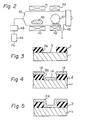
- FIG. 2 there is shown an explanatory view of one example of the apparatus for forming a metallic thin film according to the present invention.
- the reference numerals 41, 42 represent electric heaters set to temperatures of 1000°C and 400°C, respectively.
- the reference numerals 43 and 44 represent a quartz reaction tube constituting one horizontal-type reaction tube and a controller for gas flow, respectively.
- Hydrogen gas (H 2 ) as a carrier gas, is fed into the reaction tube 43.
- a gas-evacuating port 45 is connected to a booster and a vacuum rotary pump.
- the reference numerals 46 and 47 represent molten aluminum and one or more semiconductor silicon wafers, respectively. The distance between the molten aluminum 46 and the wafer 47 is 50 cm.
- the reference numeral 48 represents a container containing AICI 3 . Gaseous AICI 3 in admixture with H 2 as a carrier gas is fed into the reaction tube 43.
- Fig. 3 shows a cross sectional view of a silicon (Si) semiconductor substrate 1 on which a Si0 2 layer 2 having a thickness of about 1 11m is formed and which substrate 1 has an exposed main plane 3 formed by selectively etching the Si0 2 layer 2.
- the selective etching was carried out by a conventional reactive sputtering etching using a photoresist film (not shown) as a mask, the resultant wall or step 2a of the etched portion is almost perpendicular.
- a cross sectional view is shown in Fig. 4 of the silicon semiconductor substrate 1, shown in Fig. 3, on which an.aluminum thin film 14 having a thickness of 500 nm (5000 A) is formed by the conventional vapor deposition method. Even if the substrate were rotated during the vapor depositing procedure, it was impossible to form the aluminum thin film 14 on the wall or step 2a because of a self-shadow effect.
- the AICI released AICI 3 , whereby an aluminum thin film was deposited on the wafer 47 at a deposition rate of about 500 A/min.
- Fig. 5 shows a cross sectional view of the silicon semiconductor substrate 1 on which an aluminum thin film 24 having a thickness of 500 nm (5000A) is formed at the total pressures (P T ) of normal pressure and 1.33 x 10 3 Pa (10 Torr), respectively, by the disproportionation reaction starting from AICI 3 and Alas the raw material.
- P T total pressures
- P T total pressures
- 1.33 x 10 3 Pa (10 Torr) 1.33 x 10 3 Pa (10 Torr
Landscapes
- Chemical & Material Sciences (AREA)
- General Chemical & Material Sciences (AREA)
- Chemical Kinetics & Catalysis (AREA)
- Engineering & Computer Science (AREA)
- Materials Engineering (AREA)
- Mechanical Engineering (AREA)
- Metallurgy (AREA)
- Organic Chemistry (AREA)
- Chemical Vapour Deposition (AREA)
- Electrodes Of Semiconductors (AREA)
Claims (6)
Applications Claiming Priority (2)
| Application Number | Priority Date | Filing Date | Title |
|---|---|---|---|
| JP42209/81 | 1981-03-23 | ||
| JP56042209A JPS5948952B2 (ja) | 1981-03-23 | 1981-03-23 | 金属薄膜の形成方法 |
Publications (3)
| Publication Number | Publication Date |
|---|---|
| EP0064805A2 EP0064805A2 (fr) | 1982-11-17 |
| EP0064805A3 EP0064805A3 (en) | 1984-10-10 |
| EP0064805B1 true EP0064805B1 (fr) | 1987-08-19 |
Family
ID=12629624
Family Applications (1)
| Application Number | Title | Priority Date | Filing Date |
|---|---|---|---|
| EP82301513A Expired EP0064805B1 (fr) | 1981-03-23 | 1982-03-23 | Procédé pour produire un film mince métallique sur un corps semiconducteur |
Country Status (4)
| Country | Link |
|---|---|
| US (1) | US4430364A (fr) |
| EP (1) | EP0064805B1 (fr) |
| JP (1) | JPS5948952B2 (fr) |
| DE (1) | DE3277046D1 (fr) |
Cited By (1)
| Publication number | Priority date | Publication date | Assignee | Title |
|---|---|---|---|---|
| DE3625860A1 (de) * | 1985-08-02 | 1987-02-12 | Toshiba Kawasaki Kk | Halbleitervorrichtung mit einem kontakt und vorrichtung zur herstellung derselben |
Families Citing this family (13)
| Publication number | Priority date | Publication date | Assignee | Title |
|---|---|---|---|---|
| JPS60161235U (ja) * | 1984-04-04 | 1985-10-26 | 向川 邦彦 | 内装壁材用出隅当て枠 |
| DE3751755T2 (de) * | 1986-06-30 | 1997-04-03 | Nihon Sinku Gijutsu K K | Verfahren und Vorrichtung zum Abscheiden aus der Gasphase |
| EP0252667B1 (fr) * | 1986-06-30 | 1996-03-27 | Nihon Sinku Gijutsu Kabushiki Kaisha | Procédé de dépÔt en phase vapeur |
| GB8623788D0 (en) * | 1986-10-03 | 1986-11-05 | Emi Plc Thorn | Electrical device |
| US5023994A (en) * | 1988-09-29 | 1991-06-18 | Microwave Power, Inc. | Method of manufacturing a microwave intergrated circuit substrate including metal lined via holes |
| EP0448763A1 (fr) * | 1990-03-30 | 1991-10-02 | Siemens Aktiengesellschaft | Procédé et appareil pour la fabrication de couches ou structures conductrices pour circuits semi-conducteurs ayant la plus haute densité d'intégration |
| US5478780A (en) * | 1990-03-30 | 1995-12-26 | Siemens Aktiengesellschaft | Method and apparatus for producing conductive layers or structures for VLSI circuits |
| JPH0469526U (fr) * | 1990-10-30 | 1992-06-19 | ||
| JPH04323376A (ja) * | 1991-04-22 | 1992-11-12 | Osaka Gas Co Ltd | 酸化物薄膜の製造方法 |
| DE19730007C1 (de) * | 1997-07-12 | 1999-03-25 | Mtu Muenchen Gmbh | Verfahren und Vorrichtung zur Gasphasendiffusionsbeschichtung von Werkstücken aus warmfestem Material mit einem Beschichtungsmaterial |
| US6169031B1 (en) * | 1999-05-28 | 2001-01-02 | National Science Council | Chemical vapor deposition for titanium metal thin film |
| BRPI0414547A (pt) * | 2003-09-19 | 2006-11-07 | Akzo Nobel Nv | metalização de substrato(s) por um processo de deposição lìquido/vapor |
| JP4419062B2 (ja) * | 2004-03-29 | 2010-02-24 | ソニー株式会社 | 画像処理装置および方法、記録媒体、並びにプログラム |
Family Cites Families (6)
| Publication number | Priority date | Publication date | Assignee | Title |
|---|---|---|---|---|
| US3471321A (en) | 1964-12-30 | 1969-10-07 | Texas Instruments Inc | Vapor coating aluminum on ironcontaining substrate |
| US3801365A (en) * | 1971-08-05 | 1974-04-02 | Energy Conversion Devices Inc | Method for producing an electrical device |
| GB1436999A (en) | 1972-06-21 | 1976-05-26 | Lucas Electrical Ltd | Method of depositing aluminium on the surface of a semi- conductor wafer |
| GB1399163A (en) * | 1972-11-08 | 1975-06-25 | Ferranti Ltd | Methods of manufacturing semiconductor devices |
| GB2038883B (en) | 1978-11-09 | 1982-12-08 | Standard Telephones Cables Ltd | Metallizing semiconductor devices |
| GB2041983B (en) * | 1978-11-09 | 1982-12-01 | Standard Telephones Cables Ltd | Metallising semiconductor devices |
-
1981
- 1981-03-23 JP JP56042209A patent/JPS5948952B2/ja not_active Expired
-
1982
- 1982-03-22 US US06/360,661 patent/US4430364A/en not_active Expired - Fee Related
- 1982-03-23 EP EP82301513A patent/EP0064805B1/fr not_active Expired
- 1982-03-23 DE DE8282301513T patent/DE3277046D1/de not_active Expired
Cited By (1)
| Publication number | Priority date | Publication date | Assignee | Title |
|---|---|---|---|---|
| DE3625860A1 (de) * | 1985-08-02 | 1987-02-12 | Toshiba Kawasaki Kk | Halbleitervorrichtung mit einem kontakt und vorrichtung zur herstellung derselben |
Also Published As
| Publication number | Publication date |
|---|---|
| EP0064805A3 (en) | 1984-10-10 |
| DE3277046D1 (en) | 1987-09-24 |
| JPS5948952B2 (ja) | 1984-11-29 |
| JPS57158370A (en) | 1982-09-30 |
| EP0064805A2 (fr) | 1982-11-17 |
| US4430364A (en) | 1984-02-07 |
Similar Documents
| Publication | Publication Date | Title |
|---|---|---|
| EP0064805B1 (fr) | Procédé pour produire un film mince métallique sur un corps semiconducteur | |
| US4608271A (en) | Method for the manufacture of metal silicide layers by means of reduced pressure gas phase deposition | |
| US5306666A (en) | Process for forming a thin metal film by chemical vapor deposition | |
| US4501769A (en) | Method for selective deposition of layer structures consisting of silicides of HMP metals on silicon substrates and products so-formed | |
| EP0414267B1 (fr) | Procédé pour déposer un film de tungstène sur une plaquette semi-conductrice | |
| US5376405A (en) | Chemical vapor deposition technique for depositing titanium silicide on semiconductor wafers | |
| US7268078B2 (en) | Chemical vapor deposition of titanium from titanium tetrachloride and hydrocarbon reactants | |
| TWI480977B (zh) | 銅內連線用的氮化鈷層及其製造方法 | |
| US5747384A (en) | Process of forming a refractory metal thin film | |
| KR950004895B1 (ko) | 구리 필름을 화학 증착시키는 유기 금속 구리 착물 | |
| US4617087A (en) | Method for differential selective deposition of metal for fabricating metal contacts in integrated semiconductor circuits | |
| US5358901A (en) | Process for forming an intermetallic layer | |
| US4923715A (en) | Method of forming thin film by chemical vapor deposition | |
| EP0566040A2 (fr) | Procédé pour déposer sélectivement une alliage cuivre-aluminium sur un substrat | |
| JPH10508656A (ja) | コンフオーマルなチタン系フイルムおよびその製造方法 | |
| EP0493002B1 (fr) | Procédé de formation d'un film déposé | |
| US5277934A (en) | Method for protecting a graphite chuck for a starter filament in the manufacture of polycrystalline silicon | |
| JP3524945B2 (ja) | 被覆フィラメント | |
| JPS60145376A (ja) | タングステンシリサイド膜の成長方法 | |
| EP0397131B1 (fr) | Procédé de fabrication de contacts dans des dispositifs à semiconducteur | |
| JP3189767B2 (ja) | 銅配線の製造方法 | |
| JPH07142411A (ja) | 半導体装置における金属薄膜形成方法 | |
| JP2677230B2 (ja) | TiN膜の形成方法 | |
| JP2940162B2 (ja) | 高融点金属の気相成長法及びそれを用いた金属配線の製造方法 | |
| JPH06252051A (ja) | 金属及びメタロイド層の化学的析出方法 |
Legal Events
| Date | Code | Title | Description |
|---|---|---|---|
| PUAI | Public reference made under article 153(3) epc to a published international application that has entered the european phase |
Free format text: ORIGINAL CODE: 0009012 |
|
| AK | Designated contracting states |
Designated state(s): DE FR GB NL |
|
| PUAL | Search report despatched |
Free format text: ORIGINAL CODE: 0009013 |
|
| AK | Designated contracting states |
Designated state(s): DE FR GB NL |
|
| 17P | Request for examination filed |
Effective date: 19841214 |
|
| 17Q | First examination report despatched |
Effective date: 19860225 |
|
| GRAA | (expected) grant |
Free format text: ORIGINAL CODE: 0009210 |
|
| AK | Designated contracting states |
Kind code of ref document: B1 Designated state(s): DE FR GB |
|
| ET | Fr: translation filed | ||
| REF | Corresponds to: |
Ref document number: 3277046 Country of ref document: DE Date of ref document: 19870924 |
|
| PLBE | No opposition filed within time limit |
Free format text: ORIGINAL CODE: 0009261 |
|
| STAA | Information on the status of an ep patent application or granted ep patent |
Free format text: STATUS: NO OPPOSITION FILED WITHIN TIME LIMIT |
|
| 26N | No opposition filed | ||
| PGFP | Annual fee paid to national office [announced via postgrant information from national office to epo] |
Ref country code: FR Payment date: 19911231 Year of fee payment: 11 |
|
| PGFP | Annual fee paid to national office [announced via postgrant information from national office to epo] |
Ref country code: GB Payment date: 19920107 Year of fee payment: 11 |
|
| PGFP | Annual fee paid to national office [announced via postgrant information from national office to epo] |
Ref country code: DE Payment date: 19920522 Year of fee payment: 11 |
|
| PG25 | Lapsed in a contracting state [announced via postgrant information from national office to epo] |
Ref country code: GB Effective date: 19930323 |
|
| GBPC | Gb: european patent ceased through non-payment of renewal fee |
Effective date: 19930323 |
|
| PG25 | Lapsed in a contracting state [announced via postgrant information from national office to epo] |
Ref country code: FR Effective date: 19931130 |
|
| PG25 | Lapsed in a contracting state [announced via postgrant information from national office to epo] |
Ref country code: DE Effective date: 19931201 |
|
| REG | Reference to a national code |
Ref country code: FR Ref legal event code: ST |