EP0064872A2 - Plaquettes céramiques à circuits imprimés - Google Patents
Plaquettes céramiques à circuits imprimés Download PDFInfo
- Publication number
- EP0064872A2 EP0064872A2 EP82302346A EP82302346A EP0064872A2 EP 0064872 A2 EP0064872 A2 EP 0064872A2 EP 82302346 A EP82302346 A EP 82302346A EP 82302346 A EP82302346 A EP 82302346A EP 0064872 A2 EP0064872 A2 EP 0064872A2
- Authority
- EP
- European Patent Office
- Prior art keywords
- ceramic
- wiring board
- mgo
- sio
- holes
- Prior art date
- Legal status (The legal status is an assumption and is not a legal conclusion. Google has not performed a legal analysis and makes no representation as to the accuracy of the status listed.)
- Withdrawn
Links
Images
Classifications
-
- H—ELECTRICITY
- H05—ELECTRIC TECHNIQUES NOT OTHERWISE PROVIDED FOR
- H05K—PRINTED CIRCUITS; CASINGS OR CONSTRUCTIONAL DETAILS OF ELECTRIC APPARATUS; MANUFACTURE OF ASSEMBLAGES OF ELECTRICAL COMPONENTS
- H05K1/00—Printed circuits
- H05K1/02—Details
- H05K1/09—Use of materials for the conductive, e.g. metallic pattern
- H05K1/092—Dispersed materials, e.g. conductive pastes or inks
-
- H—ELECTRICITY
- H05—ELECTRIC TECHNIQUES NOT OTHERWISE PROVIDED FOR
- H05K—PRINTED CIRCUITS; CASINGS OR CONSTRUCTIONAL DETAILS OF ELECTRIC APPARATUS; MANUFACTURE OF ASSEMBLAGES OF ELECTRICAL COMPONENTS
- H05K1/00—Printed circuits
- H05K1/02—Details
- H05K1/03—Use of materials for the substrate
- H05K1/0306—Inorganic insulating substrates, e.g. ceramic, glass
-
- H—ELECTRICITY
- H10—SEMICONDUCTOR DEVICES; ELECTRIC SOLID-STATE DEVICES NOT OTHERWISE PROVIDED FOR
- H10W—GENERIC PACKAGES, INTERCONNECTIONS, CONNECTORS OR OTHER CONSTRUCTIONAL DETAILS OF DEVICES COVERED BY CLASS H10
- H10W70/00—Package substrates; Interposers; Redistribution layers [RDL]
- H10W70/60—Insulating or insulated package substrates; Interposers; Redistribution layers
- H10W70/611—Insulating or insulated package substrates; Interposers; Redistribution layers for connecting multiple chips together
-
- H—ELECTRICITY
- H10—SEMICONDUCTOR DEVICES; ELECTRIC SOLID-STATE DEVICES NOT OTHERWISE PROVIDED FOR
- H10W—GENERIC PACKAGES, INTERCONNECTIONS, CONNECTORS OR OTHER CONSTRUCTIONAL DETAILS OF DEVICES COVERED BY CLASS H10
- H10W70/00—Package substrates; Interposers; Redistribution layers [RDL]
- H10W70/60—Insulating or insulated package substrates; Interposers; Redistribution layers
- H10W70/62—Insulating or insulated package substrates; Interposers; Redistribution layers characterised by their interconnections
- H10W70/63—Vias, e.g. via plugs
- H10W70/635—Through-vias
-
- H—ELECTRICITY
- H10—SEMICONDUCTOR DEVICES; ELECTRIC SOLID-STATE DEVICES NOT OTHERWISE PROVIDED FOR
- H10W—GENERIC PACKAGES, INTERCONNECTIONS, CONNECTORS OR OTHER CONSTRUCTIONAL DETAILS OF DEVICES COVERED BY CLASS H10
- H10W70/00—Package substrates; Interposers; Redistribution layers [RDL]
- H10W70/60—Insulating or insulated package substrates; Interposers; Redistribution layers
- H10W70/62—Insulating or insulated package substrates; Interposers; Redistribution layers characterised by their interconnections
- H10W70/66—Conductive materials thereof
- H10W70/666—Organic materials or pastes
-
- H—ELECTRICITY
- H10—SEMICONDUCTOR DEVICES; ELECTRIC SOLID-STATE DEVICES NOT OTHERWISE PROVIDED FOR
- H10W—GENERIC PACKAGES, INTERCONNECTIONS, CONNECTORS OR OTHER CONSTRUCTIONAL DETAILS OF DEVICES COVERED BY CLASS H10
- H10W70/00—Package substrates; Interposers; Redistribution layers [RDL]
- H10W70/60—Insulating or insulated package substrates; Interposers; Redistribution layers
- H10W70/67—Insulating or insulated package substrates; Interposers; Redistribution layers characterised by their insulating layers or insulating parts
- H10W70/69—Insulating materials thereof
-
- H—ELECTRICITY
- H05—ELECTRIC TECHNIQUES NOT OTHERWISE PROVIDED FOR
- H05K—PRINTED CIRCUITS; CASINGS OR CONSTRUCTIONAL DETAILS OF ELECTRIC APPARATUS; MANUFACTURE OF ASSEMBLAGES OF ELECTRICAL COMPONENTS
- H05K3/00—Apparatus or processes for manufacturing printed circuits
- H05K3/46—Manufacturing multilayer circuits
- H05K3/4611—Manufacturing multilayer circuits by laminating two or more circuit boards
-
- H—ELECTRICITY
- H05—ELECTRIC TECHNIQUES NOT OTHERWISE PROVIDED FOR
- H05K—PRINTED CIRCUITS; CASINGS OR CONSTRUCTIONAL DETAILS OF ELECTRIC APPARATUS; MANUFACTURE OF ASSEMBLAGES OF ELECTRICAL COMPONENTS
- H05K3/00—Apparatus or processes for manufacturing printed circuits
- H05K3/46—Manufacturing multilayer circuits
- H05K3/4611—Manufacturing multilayer circuits by laminating two or more circuit boards
- H05K3/4626—Manufacturing multilayer circuits by laminating two or more circuit boards characterised by the insulating layers or materials
- H05K3/4629—Manufacturing multilayer circuits by laminating two or more circuit boards characterised by the insulating layers or materials laminating inorganic sheets comprising printed circuits, e.g. green ceramic sheets
-
- Y—GENERAL TAGGING OF NEW TECHNOLOGICAL DEVELOPMENTS; GENERAL TAGGING OF CROSS-SECTIONAL TECHNOLOGIES SPANNING OVER SEVERAL SECTIONS OF THE IPC; TECHNICAL SUBJECTS COVERED BY FORMER USPC CROSS-REFERENCE ART COLLECTIONS [XRACs] AND DIGESTS
- Y10—TECHNICAL SUBJECTS COVERED BY FORMER USPC
- Y10S—TECHNICAL SUBJECTS COVERED BY FORMER USPC CROSS-REFERENCE ART COLLECTIONS [XRACs] AND DIGESTS
- Y10S428/00—Stock material or miscellaneous articles
- Y10S428/901—Printed circuit
-
- Y—GENERAL TAGGING OF NEW TECHNOLOGICAL DEVELOPMENTS; GENERAL TAGGING OF CROSS-SECTIONAL TECHNOLOGIES SPANNING OVER SEVERAL SECTIONS OF THE IPC; TECHNICAL SUBJECTS COVERED BY FORMER USPC CROSS-REFERENCE ART COLLECTIONS [XRACs] AND DIGESTS
- Y10—TECHNICAL SUBJECTS COVERED BY FORMER USPC
- Y10T—TECHNICAL SUBJECTS COVERED BY FORMER US CLASSIFICATION
- Y10T29/00—Metal working
- Y10T29/49—Method of mechanical manufacture
- Y10T29/49002—Electrical device making
- Y10T29/49117—Conductor or circuit manufacturing
- Y10T29/49124—On flat or curved insulated base, e.g., printed circuit, etc.
- Y10T29/49155—Manufacturing circuit on or in base
- Y10T29/49163—Manufacturing circuit on or in base with sintering of base
-
- Y—GENERAL TAGGING OF NEW TECHNOLOGICAL DEVELOPMENTS; GENERAL TAGGING OF CROSS-SECTIONAL TECHNOLOGIES SPANNING OVER SEVERAL SECTIONS OF THE IPC; TECHNICAL SUBJECTS COVERED BY FORMER USPC CROSS-REFERENCE ART COLLECTIONS [XRACs] AND DIGESTS
- Y10—TECHNICAL SUBJECTS COVERED BY FORMER USPC
- Y10T—TECHNICAL SUBJECTS COVERED BY FORMER US CLASSIFICATION
- Y10T428/00—Stock material or miscellaneous articles
- Y10T428/24—Structurally defined web or sheet [e.g., overall dimension, etc.]
- Y10T428/24273—Structurally defined web or sheet [e.g., overall dimension, etc.] including aperture
- Y10T428/24322—Composite web or sheet
- Y10T428/24331—Composite web or sheet including nonapertured component
Definitions
- This invention relates to ceramic wiring boards and more particularly to wiring boards wherein at least the conductor filled in through-hole parts of ceramic substrates is improved.
- ceramic wiring boards have been made by screen printing a wiring pattern with a conductor paste containing a metal powder selected from W powder and Mo powder as a conductive component on a ceramic green sheet mainly composed of A1 2 0 3 and then sintering this green sheet.
- Multilayer ceramic wiring boards have been made by the following steps (a) - (g). That is, (a) mixing a mixture of A1 2 0 3 powder and a sintering assistant which is molten at 1300°C - 1500°C, e.g., powder of at least one compound selected from SiO 2 -Mg0-Al 2 O 3 low melting compounds, kaolinite and dolomite with an organic binder, e.g., butyral, polyvinyl alcohol, etc. and an organic solvent, e.g., trichloroethylene, alcohols, etc.
- a sintering assistant which is molten at 1300°C - 1500°C
- an organic binder e.g., butyral, polyvinyl alcohol, etc.
- an organic solvent e.g., trichloroethylene, alcohols, etc.
- the green sheet part is sintered with great contraction at temperatures from melting temperature of the sintering assistant to sintering temperature of A1 2 0 3 and the wiring pattern part into which the sintering assistant penetrates from the surrounding green sheet part is also sintered with a great contraction like the green sheet part.
- the conductor paste part is not sufficiently sintered as compared with the green sheet part and hence does not become dense and furthermore contraction of the paste part is small and hence a large strain remains in the vicinity of the through-holes after sintering, which causes cracks and warpage of the wiring board.
- plating solution penetrates into the sintered conductor in the through-holes and this plating solution corrodes the through-holes to result in high resistance and finally disconnection.
- the object of this invention is to provide a ceramic wiring board which shows neither warp nor crack of ceramic substrates and furthermore which shows no corrosion of the sintered conductor in the through-holes.
- the above object can be attained by using at least the sintered conductor part filled in the through-holes which comprises a metal and the same compound as the sintering assistant used in the ceramic substrate.
- the sintered conductor filled in the through-holes comprises said components, no strain is present in the vicinity of the through-holes and the conductor becomes dense. Thus, no warp and crack of ceramic substrates occur and no defective products are produced. Furthermore, since the sintered conductor filled in the through-holes is not corroded, disconnection of the sintered wiring conductor does not occur during use and reliability is increased.
- the ceramic substrates comprise (a) as ceramic a metal oxide selected from Al 2 O 3 (m.p. 2015°C), MgO (m.p. 2800°C), SiO 2 (m.p. 1273°C), ZrO 2 (m.p. 2677°C) and BeO (m.p. 2550°C) or a compound selected fromnitee (3Al 2 O 3 -2SiO 2 , m.p. 1830°C), forsterite (2MgO.SiO 2 , m.p. 1900°C) and steatite (MgO.SiO 2 , m.p.
- SiO 2 -MgO-Al 2 O 3 low melting compounds e.g., cordierite (2MgO. 2Al 2 O 3 ⁇ 5SiO 2 , m. p. 1500°C), SiO 2 -MgO-CaO low melting compounds, e.g., diopside ⁇ (Ca, Mg)O.MgO.2SiO 2 , m.p. 1400°C ⁇ , Al 2 O 3 -SiO 2 minerals, e.g., kaolinite (Al 2 O 3 ⁇ 2SiO 2 ⁇ 2H 2 0, m.p.
- SiO 2 -MgO-Al 2 O 3 low melting compounds e.g., cordierite (2MgO. 2Al 2 O 3 ⁇ 5SiO 2 , m. p. 1500°C)
- SiO 2 -MgO-CaO low melting compounds e.g., diopside ⁇ (Ca, Mg)O
- MgO-CaO minerals e.g., dolomite ⁇ (M g , Ca)(CO 3 ) 2 , m. p. 2370°C ⁇
- MgO-SiO 2 minerals e.g., talc (3MgO ⁇ 4SiO 2 ⁇ H 2 O, m.p. 1543°C).
- a sintering acceleration effect is recognized with 99.9 wt% or less of said ceramic (a) and 0.1 wt% or more of said sintering assistant (b), but preferred mixing ratio for obtaining sufficient effect of lowering the sintering temperature is 80 - 95 wt% of said ceramic (a) and 20 - 5 wt% of said sintering assistant (b).
- the conductor paste comprises (c) a metal powder selected from W powder and Mo powder, (b) a sintering assistant mentioned hereinabove with reference to the ceramic substrates, (d) an organic binder, e.g., nitrocellulose, ethylcellulose and (e) an organic solvent, e.g., a-terpineol, n-butyl carbitol acetate.
- a metal powder selected from W powder and Mo powder
- a sintering assistant mentioned hereinabove with reference to the ceramic substrates e.g., nitrocellulose, ethylcellulose and (e) an organic solvent, e.g., a-terpineol, n-butyl carbitol acetate.
- The.mixing ratio of said sintering assistant (b) and said metal powders (c) is 0.5 - 20 wt% of the former and 99.5 - 80 wt% of the latter.
- amount of the sintering assistant (b) is less than 0.5 wt%, sufficient sintering effect cannot be obtained and when more than 20 wt%, conductivity is extremely damaged.
- the organic binder (d) and the organic solvent (e) are organic materials necessary for obtaining a conductive paste using the sintering assistant powder (b) and the metal powder (c).
- Mixing ratios of the organic binder (d) and the organic solvent (e) to the total amount of the sintering assistant powder (b) and the metal powder (c) are 5 - 10 wt% and 60 - 75 wt% to 20 - 30 wt% of (b) + (c), respectively.
- Viscosity of the paste prepared at such mixing ratios is the viscosity suitable for printing, for example, 10 3 - 10 4 poises by shear rate (1/sec).
- a mixed powder comprising 80 - 95 wt% of ceramic (a) and 20 - 5 wt% of sintering assistant (b) is mixed with 5 - 10 wt% of at least one organic binder selected from butyral resin and polyvinyl alcohol and 15 - 30 wt% of at least one organic solvent selected from trichloroethylene and an alcohol to obtain a slurry material.
- This slurry material is cast by an ordinary doctor blade and heat treated at 80 - 120°C for about 30 - 3 hours to obtain a sheet-like molded material called ceramic green sheet.
- ceramic green sheet are made through-holes of 0.1 mm - 0.5 mm in diameter at the desired positions by electron beam or mechanical means such as press, punch, drill, etc.
- these through-holes is filled said conductive paste by screen printing process.
- the desired wiring pattern is formed by screen printing process on the surface of the green sheet having through-holes filled with the conductive paste.
- the conductive paste for formation of the wiring pattern may be the conductor paste mentioned hereinbefore or this conductor paste from which the sintering assistant (b) is omitted.
- a plurality of these ceramic green sheets having through-holes filled with the conductor paste and printed wiring patterns are stacked with registration so as to ensure that wirings can be connected between the sheets. Then, the stacked sheets are pressed with heat under a pressure of 5 kg/cm 2 - 40 kg/cm 2 at 80°C - 150°C for 5 minutes - 15 minutes to obtain an unsintered multi- layer wiring board.
- This unsintered multi-layer wiring board is sintered in a mixed atmosphere of N 2 , H 2 and H 2 0 at a temperature of at least the melting point of said sintering assistant (b) and less than the melting point of said ceramic (a), e.g., at 1500°C - 1600°C when Al 2 O 3 is used as the compound (a) and cordierite as said sintering assistant (b).
- Composition of the atmosphere gas is usually N 2 : 70 - 80 vol%, H 2 : 15 - 20 vol% and H 2 0: 5 - 10 vol%.
- Heating rate at the sintering is usually 50 - 200 °C/hr and retention time at maximum temperature is usually about 0.5 - 2 hours.
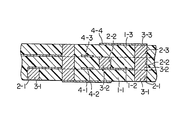
- Figure is a partial cross-sectional view of the ceramic multi-layer wiring board.
- a conductor paste prepared by homogeneously mixing 25 g of a mixed powder comprising 90 wt% of W powder having a mean particle diameter of 2 ⁇ m, 6 wt% of talc powder having a mean particle diameter of 5 ⁇ m and 4 wt% of kaolinite powder having a mean particle diameter of 3 um, 8 g of ethylcellulose and 67 g of a-terpineol, through-holes 2-1, 2-2 and 2-3 were filled with this conductor paste, namely, 3-1, 3-2 and 3-3 and simultaneously the desired wiring patterns 4-1, 4-2, 4-3 and 4-4 were formed.
- This unsintered multi-layer wiring board was sintered in an atmosphere of N 2 : 75 vol%, H 2 : 17 vol% and H 2 0: 8 vol% by heating it at a temperature of 1600°C at a heating rate of 130°C/hr and retaining it at the sintering temperature for 1.5 hour to obtain a multi-layer ceramic wiring board.
- This multi-layer ceramic wiring board was subjected to a thermal shock test 50 times, which comprised leaving it to stand at 0°C for 1 hour and then at 100°C for 1 hour to find that 0.01% of cracks occurred at the through-hole part.
- a thermal shock test 50 times, which comprised leaving it to stand at 0°C for 1 hour and then at 100°C for 1 hour to find that 0.01% of cracks occurred at the through-hole part.
- 10 - 15% of cracks occurred at the through-hole part 10 - 15% of cracks occurred at the through-hole part.
- water absorption of said multi- layer ceramic wiring board of this invention was 0.001% while that of the conventional multi-layer ceramic wiring board was about 0.2%.
- Example 1 was repeated except that a conductor paste obtained by homogeneously mixing 20 g of a mixed powder comprising 99.5 wt% of W powder having a mean particle diameter of 2 um, 0.3 wt% of talc powder having a mean particle diameter of 5 ⁇ m and 0.2 wt% of kaolinite powder having a mean particle diameter of 3 ⁇ m, 5 g of nitrocellulose and 75 g of n-butyl carbitole acetate was used for formation of wiring patterns and filling of the through-holes.
- a multi-layer ceramic wiring board was made in the same manner as in Example 1 except that a conductor paste obtained by homogeneously mixing 30 g of a mixed powder which comprised 80 wt% of Mo powder having a mean particle diameter of 2 ⁇ m, 10 wt% of talc powder having a mean particle diameter of 5 ⁇ m and 10 wt% of kaolinite powder having a mean particle diameter of 3 ⁇ m, 10 g of ethylcellulose and 60 g of a-terpineol was used for formation of the wiring patterns and filling of the through-holes.
- This multi-layer ceramic wiring board had good characteristics like that of Example 1.
- a multi-layer ceramic wiring board was made in the same manner as in Example 1 except that a slurry material comprising 65 wt% of a mixture of 80 wt% of A1 2 0 3 powder having a mean particle diameter of 4 pm, 10 wt% of talc powder having a mean particle diameter of 5 ⁇ m and 10 wt% of kaolinite powder having a mean particle diameter of 3 ⁇ m, 5 wt% of polyvinyl alcohol and 30 wt% of ethyl alcohol was used for producing the green sheets; pressure, heating temperature and heating time at production of the unsintered multi-layer ceramic wiring board were 5 kg/cm 2 , 150°C and 15 minutes, respectively; sintering atmosphere comprised N 2 : 70 vol%, H 2 : 20 vol% and H 2 0: 10 vol%; heating rate was 50°C/hr, sintered temperature was 1510°C; and retention time at the sintering temperature was 0.5 hr.
- a slurry material comprising 65
- a multi-layer ceramic wiring board was produced in the same manner as in Example 1 except that a slurry material comprising 75 wt% of a mixture of 95 wt% of A1 2 0 3 powder having a particle diameter of 4 ⁇ m and 5 wt% of talc powder having a mean particle diameter or 5 ⁇ m, 10 wt% of polyvinyl alcohol and 15 wt% of ethyl alcohol was used for production of the green sheets; pressure, heating temperature and heating time at production of unsintered multi-layer ceramic wiring board were 40 kg/cm 2 , 80°C and 5 minute, respectively; sintering atmosphere comprised N 2 : 80 vol%, H 2 : 45 vol% and H 2 0: 5 vol%; heating rate was 200°C/hr, sintering temperature was 1650°C; and retention time at the sintering temperature was 2 hours.
- a slurry material comprising 75 wt% of a mixture of 95 wt% of A1 2 0 3 powder having
- a multi-layer ceramic wiring board was produced in the same manner as in Example 1 except that a homogeneous mixture of 25 g of W powder having a mean particle diameter of 2 ⁇ m, 8 g of ethylcellulose and 67 g of a-terpineol was used as the conductor paste for formation of wiring patterns.
- This wiring board had good characteristics like that of Example 1.
- Example 1 In the same manner as in Example 1, a ceramic green sheet having through-holes filled with the conductor paste and wiring patterns printed thereon was produced. This ceramic green sheet was sintered in the same manner as in Example 1 except that it was not pressed, to obtain 1 a ceramic wiring board. This ceramic wire board had good characteristics like that of Example 1.
Landscapes
- Engineering & Computer Science (AREA)
- Chemical & Material Sciences (AREA)
- Microelectronics & Electronic Packaging (AREA)
- Ceramic Engineering (AREA)
- Inorganic Chemistry (AREA)
- Dispersion Chemistry (AREA)
- Production Of Multi-Layered Print Wiring Board (AREA)
- Laminated Bodies (AREA)
- Compositions Of Oxide Ceramics (AREA)
- Printing Elements For Providing Electric Connections Between Printed Circuits (AREA)
Applications Claiming Priority (2)
| Application Number | Priority Date | Filing Date | Title |
|---|---|---|---|
| JP56068889A JPS57184296A (en) | 1981-05-09 | 1981-05-09 | Ceramic circuit board |
| JP68889/81 | 1981-05-09 |
Publications (2)
| Publication Number | Publication Date |
|---|---|
| EP0064872A2 true EP0064872A2 (fr) | 1982-11-17 |
| EP0064872A3 EP0064872A3 (fr) | 1983-08-31 |
Family
ID=13386668
Family Applications (1)
| Application Number | Title | Priority Date | Filing Date |
|---|---|---|---|
| EP82302346A Withdrawn EP0064872A3 (fr) | 1981-05-09 | 1982-05-07 | Plaquettes céramiques à circuits imprimés |
Country Status (3)
| Country | Link |
|---|---|
| US (1) | US4465727A (fr) |
| EP (1) | EP0064872A3 (fr) |
| JP (1) | JPS57184296A (fr) |
Cited By (3)
| Publication number | Priority date | Publication date | Assignee | Title |
|---|---|---|---|---|
| WO1988001469A1 (fr) * | 1986-08-15 | 1988-02-25 | Digital Equipment Corporation | Procede pour fabriquer des substrats d'interconnexion a haute densite a l'aide de modules empiles, et substrats obtenus |
| EP0220508A3 (en) * | 1985-09-27 | 1989-04-26 | Nec Corporation | A multi-layer circuit board having a large heat dissipation |
| EP0276004A3 (fr) * | 1987-01-22 | 1991-06-12 | Matsushita Electric Industrial Co., Ltd. | Substrat multicouche en céramique et son procédé de fabrication |
Families Citing this family (36)
| Publication number | Priority date | Publication date | Assignee | Title |
|---|---|---|---|---|
| JPS599992A (ja) * | 1982-07-08 | 1984-01-19 | 株式会社日立製作所 | 多層配線基板の製造方法 |
| JPS5911700A (ja) * | 1982-07-12 | 1984-01-21 | 株式会社日立製作所 | セラミツク多層配線回路板 |
| JPS5944797A (ja) * | 1982-09-07 | 1984-03-13 | 増田 閃一 | 物体の静電的処理装置 |
| JPS6014494A (ja) * | 1983-07-04 | 1985-01-25 | 株式会社日立製作所 | セラミツク多層配線基板およびその製造方法 |
| KR900004379B1 (ko) * | 1983-09-16 | 1990-06-23 | 마쯔시다덴기산교 가부시기가이샤 | 세라믹 다층기판 및 그 제조방법 |
| JPS60116191A (ja) * | 1983-11-29 | 1985-06-22 | イビデン株式会社 | 電子部品搭載用基板の製造方法 |
| FR2556503B1 (fr) * | 1983-12-08 | 1986-12-12 | Eurofarad | Substrat d'interconnexion en alumine pour composant electronique |
| JPS60254697A (ja) * | 1984-05-31 | 1985-12-16 | 富士通株式会社 | 多層セラミック回路基板および製法 |
| JPS6114187A (ja) * | 1984-06-27 | 1986-01-22 | 日本特殊陶業株式会社 | 補強板状焼結体 |
| FR2567684B1 (fr) * | 1984-07-10 | 1988-11-04 | Nec Corp | Module ayant un substrat ceramique multicouche et un circuit multicouche sur ce substrat et procede pour sa fabrication |
| JPS6183674A (ja) * | 1984-10-01 | 1986-04-28 | 株式会社日立製作所 | セラミツク配線基板及びその製造方法 |
| JPS61155243A (ja) * | 1984-12-28 | 1986-07-14 | 富士通株式会社 | グリ−ンシ−ト組成物 |
| US4724305A (en) * | 1986-03-07 | 1988-02-09 | Hitachi Metals, Ltd. | Directly-heating roller for fuse-fixing toner images |
| US4776070A (en) * | 1986-03-12 | 1988-10-11 | Hitachi Metals, Ltd. | Directly-heating roller for fixing toner images |
| WO1988005959A1 (fr) * | 1987-02-04 | 1988-08-11 | Coors Porcelain Company | Substrat ceramique presentant des passages remplis d'une substance conductrice et procede de production |
| US4799984A (en) * | 1987-09-18 | 1989-01-24 | E. I. Du Pont De Nemours And Company | Method for fabricating multilayer circuits |
| JPH0772092B2 (ja) * | 1988-02-10 | 1995-08-02 | 日本特殊陶業株式会社 | 低温焼成基板 |
| US4806188A (en) * | 1988-03-04 | 1989-02-21 | E. I. Du Pont De Nemours And Company | Method for fabricating multilayer circuits |
| JPH02148789A (ja) * | 1988-03-11 | 1990-06-07 | Internatl Business Mach Corp <Ibm> | 電子回路基板 |
| US5013605A (en) * | 1988-08-11 | 1991-05-07 | Gritz David N | Cordierite-type glass-ceramic with controlled coloration |
| US5044966A (en) * | 1989-05-23 | 1991-09-03 | Peter Friesen | Electrical panel for physically supporting and electrically connecting electrical components |
| JP2665561B2 (ja) * | 1989-09-26 | 1997-10-22 | 日本特殊陶業株式会社 | セラミック多層基板 |
| US5157477A (en) * | 1990-01-10 | 1992-10-20 | International Business Machines Corporation | Matched impedance vertical conductors in multilevel dielectric laminated wiring |
| JP2794960B2 (ja) * | 1991-02-19 | 1998-09-10 | 松下電器産業株式会社 | 焼結導体配線基板とその製造方法 |
| JP3338527B2 (ja) * | 1992-10-07 | 2002-10-28 | 富士通株式会社 | 高密度積層形のコネクタ、及び、コネクタの設計方法 |
| US5698015A (en) * | 1995-05-19 | 1997-12-16 | Nikko Company | Conductor paste for plugging through-holes in ceramic circuit boards and a ceramic circuit board having this conductor paste |
| JP3165779B2 (ja) * | 1995-07-18 | 2001-05-14 | 株式会社トクヤマ | サブマウント |
| KR100298897B1 (ko) * | 1998-12-23 | 2001-09-22 | 이형도 | 인쇄회로기판제조방법 |
| JP2000244123A (ja) * | 1999-02-19 | 2000-09-08 | Hitachi Ltd | 多層セラミック回路基板 |
| KR20030074582A (ko) * | 2003-09-03 | 2003-09-19 | 학교법인 한국정보통신학원 | 초고주파 다층회로 구조 및 제작 방법 |
| JP4518885B2 (ja) * | 2004-09-09 | 2010-08-04 | 京セラ株式会社 | セラミック電子部品及びその製造方法 |
| CN1906715B (zh) * | 2004-12-20 | 2010-06-16 | 株式会社村田制作所 | 层压陶瓷电子元件及其制造方法 |
| JP4650794B2 (ja) * | 2005-07-01 | 2011-03-16 | 昭栄化学工業株式会社 | 積層電子部品用導体ペーストおよびそれを用いた積層電子部品 |
| US7736544B2 (en) * | 2007-04-26 | 2010-06-15 | E. I. Du Pont De Nemours And Company | Electrically conductive composition for via-holes |
| US20090047569A1 (en) * | 2007-08-14 | 2009-02-19 | Jain Kailash C | High strength support for solid oxide fuel cell |
| CN109511218A (zh) * | 2018-12-16 | 2019-03-22 | 天津荣事顺发电子有限公司 | 一种多层陶瓷电路板制备方法 |
Family Cites Families (4)
| Publication number | Priority date | Publication date | Assignee | Title |
|---|---|---|---|---|
| FR2280957A1 (fr) * | 1974-08-01 | 1976-02-27 | Ibm | Composition conductrice pour metallisation, support ceramique revetu de cette composition et procede de formation |
| JPS5328266A (en) * | 1976-08-13 | 1978-03-16 | Fujitsu Ltd | Method of producing multilayer ceramic substrate |
| GB2040589B (en) * | 1978-06-28 | 1982-12-08 | Mitsumi Electric Co Ltd | Printed circuit device |
| US4345955A (en) * | 1980-10-28 | 1982-08-24 | E. I. Du Pont De Nemours And Company | Process for manufacturing multilayer ceramic chip carrier modules |
-
1981
- 1981-05-09 JP JP56068889A patent/JPS57184296A/ja active Granted
-
1982
- 1982-05-04 US US06/374,874 patent/US4465727A/en not_active Expired - Lifetime
- 1982-05-07 EP EP82302346A patent/EP0064872A3/fr not_active Withdrawn
Cited By (5)
| Publication number | Priority date | Publication date | Assignee | Title |
|---|---|---|---|---|
| EP0220508A3 (en) * | 1985-09-27 | 1989-04-26 | Nec Corporation | A multi-layer circuit board having a large heat dissipation |
| WO1988001469A1 (fr) * | 1986-08-15 | 1988-02-25 | Digital Equipment Corporation | Procede pour fabriquer des substrats d'interconnexion a haute densite a l'aide de modules empiles, et substrats obtenus |
| AU612588B2 (en) * | 1986-08-15 | 1991-07-18 | Digital Equipment Corporation | Method of making high density interconnection substrates using stacked modules and substrates obtained |
| EP0276004A3 (fr) * | 1987-01-22 | 1991-06-12 | Matsushita Electric Industrial Co., Ltd. | Substrat multicouche en céramique et son procédé de fabrication |
| US5043223A (en) * | 1987-01-22 | 1991-08-27 | Matsushita Electric Industrial Co., Ltd. | Multilayer ceramic substrate and method for making the same |
Also Published As
| Publication number | Publication date |
|---|---|
| US4465727A (en) | 1984-08-14 |
| EP0064872A3 (fr) | 1983-08-31 |
| JPS57184296A (en) | 1982-11-12 |
| JPH0258794B2 (fr) | 1990-12-10 |
Similar Documents
| Publication | Publication Date | Title |
|---|---|---|
| US4465727A (en) | Ceramic wiring boards | |
| CA1222832A (fr) | Enlevement des residus de carbone des corps en ceramique a metal dans la masse | |
| CA1078079A (fr) | Procede de preparation de ceramique multicouche | |
| KR100295695B1 (ko) | 세라믹회로판지지기판용전기피드스루 | |
| EP0132740B1 (fr) | Procédé pour fabriquer un substrat diélectrique | |
| EP0043029B1 (fr) | Substrat céramique multicouches obtenu par frittage et procédé pour sa fabrication | |
| EP0098067A2 (fr) | Procédé pour fabriquer une structure à multi-couches en verre-céramique comprenant des conducteurs basés sur le cuivre | |
| JPS60254697A (ja) | 多層セラミック回路基板および製法 | |
| KR900008781B1 (ko) | 후막도체조성물 | |
| US4576735A (en) | Electroconductive molybdenum paste | |
| US3723176A (en) | Alumina palladium composite | |
| JPH08274433A (ja) | 銀系導電性ペースト及びそれを用いた多層セラミック回路基板 | |
| JP2657008B2 (ja) | セラミックス用メタライズ組成物 | |
| JP2872273B2 (ja) | セラミツク基板材料 | |
| JPH0685466A (ja) | 多層回路基板 | |
| JP4231316B2 (ja) | セラミック配線基板の製造方法 | |
| JP2001072473A (ja) | セラミック基板の製造方法 | |
| JPS63257107A (ja) | メタライズ組成物 | |
| JP2003002751A (ja) | セラミック部品の製造方法 | |
| JPH025026B2 (fr) | ||
| JPS61278195A (ja) | 多層回路基板及びその製造方法 | |
| EP0269063A2 (fr) | Substrat multi-couche en céramique mullite et procédé pour sa fabrication | |
| JPH06291432A (ja) | ムライトセラミック基板及びその製造方法 | |
| JPH0554718B2 (fr) | ||
| JPH05139849A (ja) | セラミツク多層基板の製造方法 |
Legal Events
| Date | Code | Title | Description |
|---|---|---|---|
| PUAI | Public reference made under article 153(3) epc to a published international application that has entered the european phase |
Free format text: ORIGINAL CODE: 0009012 |
|
| AK | Designated contracting states |
Designated state(s): DE GB |
|
| PUAL | Search report despatched |
Free format text: ORIGINAL CODE: 0009013 |
|
| AK | Designated contracting states |
Designated state(s): DE GB |
|
| 17P | Request for examination filed |
Effective date: 19840110 |
|
| STAA | Information on the status of an ep patent application or granted ep patent |
Free format text: STATUS: THE APPLICATION IS DEEMED TO BE WITHDRAWN |
|
| 18D | Application deemed to be withdrawn |
Effective date: 19860121 |
|
| RIN1 | Information on inventor provided before grant (corrected) |
Inventor name: ISHIHARA, SHOOSAKU Inventor name: TAGUCHI, NORIYUKI Inventor name: FUJITA, TSUYOSHI Inventor name: TODA, GYOZO Inventor name: KUROKI, TAKASHI |