EP0065154A2 - Biegefreundliche Leiterplatte - Google Patents
Biegefreundliche Leiterplatte Download PDFInfo
- Publication number
- EP0065154A2 EP0065154A2 EP82103672A EP82103672A EP0065154A2 EP 0065154 A2 EP0065154 A2 EP 0065154A2 EP 82103672 A EP82103672 A EP 82103672A EP 82103672 A EP82103672 A EP 82103672A EP 0065154 A2 EP0065154 A2 EP 0065154A2
- Authority
- EP
- European Patent Office
- Prior art keywords
- circuit board
- printed circuit
- electronic components
- built
- base material
- Prior art date
- Legal status (The legal status is an assumption and is not a legal conclusion. Google has not performed a legal analysis and makes no representation as to the accuracy of the status listed.)
- Withdrawn
Links
Images

Classifications
-
- H—ELECTRICITY
- H05—ELECTRIC TECHNIQUES NOT OTHERWISE PROVIDED FOR
- H05K—PRINTED CIRCUITS; CASINGS OR CONSTRUCTIONAL DETAILS OF ELECTRIC APPARATUS; MANUFACTURE OF ASSEMBLAGES OF ELECTRICAL COMPONENTS
- H05K1/00—Printed circuits
- H05K1/18—Printed circuits structurally associated with non-printed electric components
- H05K1/189—Printed circuits structurally associated with non-printed electric components characterised by the use of flexible or folded printed circuits
-
- H—ELECTRICITY
- H05—ELECTRIC TECHNIQUES NOT OTHERWISE PROVIDED FOR
- H05K—PRINTED CIRCUITS; CASINGS OR CONSTRUCTIONAL DETAILS OF ELECTRIC APPARATUS; MANUFACTURE OF ASSEMBLAGES OF ELECTRICAL COMPONENTS
- H05K1/00—Printed circuits
- H05K1/02—Details
- H05K1/0277—Bendability or stretchability details
- H05K1/028—Bending or folding regions of flexible printed circuits
-
- H—ELECTRICITY
- H05—ELECTRIC TECHNIQUES NOT OTHERWISE PROVIDED FOR
- H05K—PRINTED CIRCUITS; CASINGS OR CONSTRUCTIONAL DETAILS OF ELECTRIC APPARATUS; MANUFACTURE OF ASSEMBLAGES OF ELECTRICAL COMPONENTS
- H05K2201/00—Indexing scheme relating to printed circuits covered by H05K1/00
- H05K2201/05—Flexible printed circuits [FPCs]
- H05K2201/057—Shape retainable
-
- H—ELECTRICITY
- H05—ELECTRIC TECHNIQUES NOT OTHERWISE PROVIDED FOR
- H05K—PRINTED CIRCUITS; CASINGS OR CONSTRUCTIONAL DETAILS OF ELECTRIC APPARATUS; MANUFACTURE OF ASSEMBLAGES OF ELECTRICAL COMPONENTS
- H05K2201/00—Indexing scheme relating to printed circuits covered by H05K1/00
- H05K2201/09—Shape and layout
- H05K2201/09009—Substrate related
- H05K2201/09018—Rigid curved substrate
-
- H—ELECTRICITY
- H05—ELECTRIC TECHNIQUES NOT OTHERWISE PROVIDED FOR
- H05K—PRINTED CIRCUITS; CASINGS OR CONSTRUCTIONAL DETAILS OF ELECTRIC APPARATUS; MANUFACTURE OF ASSEMBLAGES OF ELECTRICAL COMPONENTS
- H05K2201/00—Indexing scheme relating to printed circuits covered by H05K1/00
- H05K2201/10—Details of components or other objects attached to or integrated in a printed circuit board
- H05K2201/10613—Details of electrical connections of non-printed components, e.g. special leads
- H05K2201/10621—Components characterised by their electrical contacts
- H05K2201/10651—Component having two leads, e.g. resistor, capacitor
-
- H—ELECTRICITY
- H05—ELECTRIC TECHNIQUES NOT OTHERWISE PROVIDED FOR
- H05K—PRINTED CIRCUITS; CASINGS OR CONSTRUCTIONAL DETAILS OF ELECTRIC APPARATUS; MANUFACTURE OF ASSEMBLAGES OF ELECTRICAL COMPONENTS
- H05K2203/00—Indexing scheme relating to apparatus or processes for manufacturing printed circuits covered by H05K3/00
- H05K2203/30—Details of processes not otherwise provided for in H05K2203/01 - H05K2203/17
- H05K2203/302—Bending a rigid substrate; Breaking rigid substrates by bending
-
- H—ELECTRICITY
- H05—ELECTRIC TECHNIQUES NOT OTHERWISE PROVIDED FOR
- H05K—PRINTED CIRCUITS; CASINGS OR CONSTRUCTIONAL DETAILS OF ELECTRIC APPARATUS; MANUFACTURE OF ASSEMBLAGES OF ELECTRICAL COMPONENTS
- H05K3/00—Apparatus or processes for manufacturing printed circuits
- H05K3/22—Secondary treatment of printed circuits
- H05K3/28—Applying non-metallic protective coatings
Definitions
- the present invention relates to a printed circuit board made of thin base material, which is equipped with electronic components, for installation in spatially limited devices.
- the on a slide (mm 0.3 thickness) made of a specially - len material contained traces may be bent and thus adapted to the respective position of use (substitute for cable harnesses).
- the invention has for its object to develop a circuit board which can be mechanically equipped with electronic components and soldered in the conventional method and then - when installed in the device - the contour of the device can be adapted by a bending process and thus obtain the desired shape.
- a printed circuit board of the type mentioned at the outset in that a printed circuit board consisting of a conventional base material is curved in accordance with the contour of the built-in device and in that all the components arranged on it are (preferably) longitudinal in a direction parallel to a bending axis are aligned, wherein the conductor tracks are coated with solder resist to avoid cracking when bending the circuit board.
- the circuit board can be bent well in accordance with the contour of the built-in device despite the attachment of the components, the solder resist coating of the conductor tracks avoiding cracking.
- the end face approach of the circuit board for locking in a holder of the built-in device can facilitate the precise bending of the circuit board.
- Printed circuit boards according to the invention are used where flat printed circuit boards cannot be used due to the shape of the housing due to their dimensions.
- the circuit board 1 is screwed onto the base 5 in the built-in housing 6 and with one end face 1a, on which there is an attachment 1b for locking, in the holder 4 fixedly arranged in the housing 6 is clamped, as a result of which the circuit board 1 is elastically bent and the contour of the housing 6 is adapted.
- the electronic components 2 arranged on the printed circuit board 1 are preferably aligned longitudinally in one direction parallel to a bending axis 3 shown in dashed lines and therefore stiffening of the printed circuit board 1 by the components 2 is avoided. Furthermore, the circuit board 1 is coated with (not shown) solder resist, so that these coated conductor tracks are not tinned and cracking during the bending process of the circuit board 1 is prevented.
Landscapes
- Engineering & Computer Science (AREA)
- Microelectronics & Electronic Packaging (AREA)
- Combinations Of Printed Boards (AREA)
- Telephone Set Structure (AREA)
- Structure Of Printed Boards (AREA)
- Devices For Indicating Variable Information By Combining Individual Elements (AREA)
Abstract
Description
- Die vorliegende Erfindung betrifft eine Leiterplatte aus dünnem Basismaterial, die mit elektronischen Bauteilen bestückt ist, zum Einbau in räumlich begrenzte Geräte.
- Es sind aus der Firmenschrift "Flexible gedruckte Schaltungen" der Firma Kabelwerke Reinshagen flexible gedruckte Schaltungen auf Folienbasis bekannt.
- Die auf einer Folie (0,3 mm Dicke) aus einem speziel- len Werkstoff befindlichen Leiterbahnen können gebogen und somit der jeweiligen Gebrauchslage angepaßt werden (Ersatz für Kabelbäume).
- Ihr Nachteil besteht darin, daß die Folie nicht mit elektronischen Bauelementen bestückt werden kann.
- Ferner sind Einrichtungen bekannt, bei denen zwei starre Leiterplatten durch eine auflaminierte flexible gedruckte Schaltung verbunden sind.
- Ihr Nachteil ist, daß im auflaminierten flexiblen Bereich keine elektronischen Bauelemente bestückt und gelötet werden können.
- Der Erfindung liegt die Aufgabe zugrunde, eine Leiterplatte zu entwickeln, die im herkömmlichen Verfahren mit elektronischen Bauelementen maschinell bestückbar und lötbar ist und danach - beim Einbau in das Gerät - der Kontur des Gerätes durch einen Biegevorgang angepaßt werden und damit die gewünschte Form erhalten kann.
- Diese Aufgabe wird bei einer Leiterplatte der eingangs genannten Art erfindungsgemäß dadurch gelöst, daß eine aus einem herkömmlichen Basismaterial bestehende Leiterplatte entsprechend der Kontur des Einbau-Gerätes gebogen ausgebildet ist und daß alle auf ihr angeordneten Bauelemente (vorzugsweise) längs in einer zu einer Biegeachse parallelen Richtung ausgerichtet sind, wobei die Leiterbahnen zur Vermeidung von Rißbildungen beim Biegen der Leiterplatte mit Lötstoplack überzogen sind.
- Eine vorteilhafte weitere Ausgestaltung der Erfindung ist im Unteranspruch gekennzeichnet.
- Dadurch, daß die elektronischen Bauelemente parallel zu einer Biegeachse der Leiterplatte ausgerichtet sind, läßt sich die Leiterplatte trotz der Anbringung der Bauelemente entsprechend der Kontur des Einbaugerätes gut biegen, wobei der Lötstoplacküberzug der Leiterbahnen eine Rißbildung vermeidet.
- Der Stirnseitenansatz der Leiterplatte zur Arretierung in einer Halterung des Einbau-Gerätes kann dabei die genaue Biegung der Leiterplatte erleichtern.
- Ein Ausführungsbeispiel der Erfindung ist in der Zeichnung dargestellt; darin zeigen:
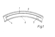
- Fig. 1 den Einbau einer gebogenen Leiterplatte in einem Handapparat eines fernmeldetechnischen Gerätes, und
- Fig. 2 die Anordnung der Bauelemente auf der Leiterplatte, wobei die gestrichelte Linie die Biegeachse andeutet.
- Wie die Fig. 1 zeigt, ist die Leiterplatte 1 im eingebauten Zustand gebogen.
- Leiterplatten nach der Erfindung werden dort eingesetzt, wo plane Leiterplatten aufgrund der Gehäuseform wegen ihrer Abmessungen nicht verwendet werden können.
- Die Leiterplatte 1 wird in dem in Fig. 1 und 2 dargestellten Ausführungsbeispiel am Sockel 5 im Einbau-Gehäuse 6 festgeschraubt und mit der einen Stirnseite 1a, an der sich ein Ansatz 1b zur Arretierung befindet, in die im Gehäuse 6 fest angeordnete Halterung 4 geklemmt, wodurch die Leiterplatte 1 elastisch gebogen und der Kontur des Gehäuses 6 angepaßt wird.
- Für die Leiterplatte 1 ist kein spezielles Basismaterial notwendig.
- Die Fig. 2 zeigt im einzelnen, daß die auf der Leiterplatte 1 angeordneten elektronischen Bauelemente 2 vorzugsweise längs in einer Richtung parallel zu einer gestrichelt dargestellten Biegeachse 3 ausgerichtet sind und daher eine Versteifung der Leiterplatte 1 durch die Bauelemente 2 vermieden wird. Ferner ist die Leiterplatte 1 mit (nicht'dargestelltem) Lötstoplack überzogen, so daß diese überzogenen Leiterbahnen nicht verzinnt werden und eine Rißbildung beim Biegevorgang der Leiterplatte 1 verhindert wird.
Claims (2)
dadurch gekennzeichnet,
daß die aus einem herkömmlichen Basismaterial bestehende Leiterplatte (1) entsprechend der Kontur des Einbau- Gerätes (6) gebogen ausgebildet ist und daß alle auf ihr angeordneten elektronischen Bauelemente (2) längs einer zu einer Biegeachse (3) parallelen Richtung ausgerichtet sind, wobei die Leiterbahnen zur Vermeidung von Rißbildungen beim Biegen der Leiterplatte (1) mit Lötstoplack überzogen sind.
dadurch gekennzeichnet,
daß die Leiterplatte (1) an ihrer Stirnseite (1a) einen Ansatz (1b) zur Arretierung in einer Halterung (4) des Einbau-Gerätes (6) aufweist.
Applications Claiming Priority (2)
| Application Number | Priority Date | Filing Date | Title |
|---|---|---|---|
| DE3119952 | 1981-05-20 | ||
| DE19813119952 DE3119952A1 (de) | 1981-05-20 | 1981-05-20 | Biegefreundliche leiterplatte mit zueinander parallel ausgerichteten bauelementen |
Publications (2)
| Publication Number | Publication Date |
|---|---|
| EP0065154A2 true EP0065154A2 (de) | 1982-11-24 |
| EP0065154A3 EP0065154A3 (de) | 1984-03-28 |
Family
ID=6132717
Family Applications (1)
| Application Number | Title | Priority Date | Filing Date |
|---|---|---|---|
| EP82103672A Withdrawn EP0065154A3 (de) | 1981-05-20 | 1982-04-29 | Biegefreundliche Leiterplatte |
Country Status (5)
| Country | Link |
|---|---|
| EP (1) | EP0065154A3 (de) |
| AU (1) | AU552487B2 (de) |
| DE (1) | DE3119952A1 (de) |
| GB (1) | GB2098809B (de) |
| SG (1) | SG66384G (de) |
Cited By (2)
| Publication number | Priority date | Publication date | Assignee | Title |
|---|---|---|---|---|
| EP0199007A3 (de) * | 1985-04-23 | 1988-07-27 | Bodenseewerk Gerätetechnik GmbH | Trägerplattenanordnung für hohe Beschleunigungen |
| US9770571B2 (en) | 1996-10-16 | 2017-09-26 | Resmed Limited | Vent valve assembly |
Family Cites Families (3)
| Publication number | Priority date | Publication date | Assignee | Title |
|---|---|---|---|---|
| US3499220A (en) * | 1967-02-28 | 1970-03-10 | Amerace Esna Corp | Method of and apparatus for making a flexible,printed electrical circuit |
| US4136225A (en) * | 1977-07-08 | 1979-01-23 | Bell Telephone Laboratories, Incorporated | Cover coatings for printed circuits |
| GB1545531A (en) * | 1977-09-07 | 1979-05-10 | Gould Advance Ltd | Electronic assemblies |
-
1981
- 1981-05-20 DE DE19813119952 patent/DE3119952A1/de not_active Withdrawn
-
1982
- 1982-04-29 EP EP82103672A patent/EP0065154A3/de not_active Withdrawn
- 1982-05-03 AU AU83223/82A patent/AU552487B2/en not_active Ceased
- 1982-05-13 GB GB8213932A patent/GB2098809B/en not_active Expired
-
1984
- 1984-09-18 SG SG66384A patent/SG66384G/en unknown
Cited By (2)
| Publication number | Priority date | Publication date | Assignee | Title |
|---|---|---|---|---|
| EP0199007A3 (de) * | 1985-04-23 | 1988-07-27 | Bodenseewerk Gerätetechnik GmbH | Trägerplattenanordnung für hohe Beschleunigungen |
| US9770571B2 (en) | 1996-10-16 | 2017-09-26 | Resmed Limited | Vent valve assembly |
Also Published As
| Publication number | Publication date |
|---|---|
| EP0065154A3 (de) | 1984-03-28 |
| GB2098809B (en) | 1984-08-15 |
| AU8322382A (en) | 1982-11-25 |
| SG66384G (en) | 1985-03-15 |
| GB2098809A (en) | 1982-11-24 |
| DE3119952A1 (de) | 1982-12-09 |
| AU552487B2 (en) | 1986-06-05 |
Similar Documents
| Publication | Publication Date | Title |
|---|---|---|
| DE3790062C2 (de) | ||
| DE3535923A1 (de) | Substrathaltender aufbau | |
| DE60128537T2 (de) | Zusammenbau zur verbindung von mindestens zwei gedruckten schaltungen | |
| DE1925791A1 (de) | Montagetafel fuer integrierte Schaltungen | |
| DE60003261T2 (de) | Elektrisches Verbindersystem für Flachkabel | |
| DE1791205B2 (de) | In einen Aufnahmerahmen eines Gerätes der elektrischen Nachrichtenoder Meßtechnik einschiebbare Baugruppe | |
| EP0065154A2 (de) | Biegefreundliche Leiterplatte | |
| DE3919273C2 (de) | Leiterplattenanordnung | |
| DE202015008007U1 (de) | Leiterplattenanordnung | |
| DE2948319C2 (de) | Verfahren zum Anbringen und Befestigen von Stromzuführungsdrähten an elektrischen Bauelementen | |
| DE1591581C3 (de) | Mikrowellen-Schattkreis in Triplate-Technik | |
| DE3329651C2 (de) | ||
| DE29621580U1 (de) | Leitungs-Steckverbindung | |
| DE8114897U1 (de) | Biegefreundliche leiterplatte mit zueinander parallel ausgerichteten bauelementen | |
| DE3925157C2 (de) | ||
| DE3316286A1 (de) | Vorrichtung zum kontaktieren von leiterplatten | |
| DE3211466C2 (de) | Leiterplattenanordnung | |
| DE10342047A1 (de) | Elektrisches Verbindungselement | |
| DE19613587C2 (de) | Anordnung zur Blockierung der elektromagnetischen Abstrahlung bei Leiterkarten und integrierten Schaltkreisen | |
| DE3133199C2 (de) | Kontaktsokel für elektrische Bauteile | |
| DE3046123C2 (de) | Steckverbinder zum Verbinden der Leiterbahnen von Leiterplatten | |
| DE4008542A1 (de) | Verfahren zum aendern von gedruckten leiterplatten | |
| DE7908303U1 (de) | Halter für Kühlbleche für elektronische Bauteile in einem Gerätechassis | |
| DE2652951A1 (de) | Schaltungsanordnung mit einer leiterplatte und darauf angeordneten bauelementen | |
| DE29514440U1 (de) | Leiterplatte für ein elektrisches oder elektronisches Gerät |
Legal Events
| Date | Code | Title | Description |
|---|---|---|---|
| PUAI | Public reference made under article 153(3) epc to a published international application that has entered the european phase |
Free format text: ORIGINAL CODE: 0009012 |
|
| AK | Designated contracting states |
Designated state(s): AT BE CH FR IT LU NL SE |
|
| PUAL | Search report despatched |
Free format text: ORIGINAL CODE: 0009013 |
|
| AK | Designated contracting states |
Designated state(s): AT BE CH FR IT LI LU NL SE |
|
| 17P | Request for examination filed |
Effective date: 19840330 |
|
| 17Q | First examination report despatched |
Effective date: 19860710 |
|
| RAP1 | Party data changed (applicant data changed or rights of an application transferred) |
Owner name: KRONE AKTIENGESELLSCHAFT |
|
| STAA | Information on the status of an ep patent application or granted ep patent |
Free format text: STATUS: THE APPLICATION HAS BEEN WITHDRAWN |
|
| 18W | Application withdrawn |
Withdrawal date: 19870121 |
|
| RIN1 | Information on inventor provided before grant (corrected) |
Inventor name: BECKER, PETER |