EP0065154A2 - Plaquette de circuit apte au cintrage - Google Patents
Plaquette de circuit apte au cintrage Download PDFInfo
- Publication number
- EP0065154A2 EP0065154A2 EP82103672A EP82103672A EP0065154A2 EP 0065154 A2 EP0065154 A2 EP 0065154A2 EP 82103672 A EP82103672 A EP 82103672A EP 82103672 A EP82103672 A EP 82103672A EP 0065154 A2 EP0065154 A2 EP 0065154A2
- Authority
- EP
- European Patent Office
- Prior art keywords
- circuit board
- printed circuit
- electronic components
- built
- base material
- Prior art date
- Legal status (The legal status is an assumption and is not a legal conclusion. Google has not performed a legal analysis and makes no representation as to the accuracy of the status listed.)
- Withdrawn
Links
Images

Classifications
-
- H—ELECTRICITY
- H05—ELECTRIC TECHNIQUES NOT OTHERWISE PROVIDED FOR
- H05K—PRINTED CIRCUITS; CASINGS OR CONSTRUCTIONAL DETAILS OF ELECTRIC APPARATUS; MANUFACTURE OF ASSEMBLAGES OF ELECTRICAL COMPONENTS
- H05K1/00—Printed circuits
- H05K1/18—Printed circuits structurally associated with non-printed electric components
- H05K1/189—Printed circuits structurally associated with non-printed electric components characterised by the use of flexible or folded printed circuits
-
- H—ELECTRICITY
- H05—ELECTRIC TECHNIQUES NOT OTHERWISE PROVIDED FOR
- H05K—PRINTED CIRCUITS; CASINGS OR CONSTRUCTIONAL DETAILS OF ELECTRIC APPARATUS; MANUFACTURE OF ASSEMBLAGES OF ELECTRICAL COMPONENTS
- H05K1/00—Printed circuits
- H05K1/02—Details
- H05K1/0277—Bendability or stretchability details
- H05K1/028—Bending or folding regions of flexible printed circuits
-
- H—ELECTRICITY
- H05—ELECTRIC TECHNIQUES NOT OTHERWISE PROVIDED FOR
- H05K—PRINTED CIRCUITS; CASINGS OR CONSTRUCTIONAL DETAILS OF ELECTRIC APPARATUS; MANUFACTURE OF ASSEMBLAGES OF ELECTRICAL COMPONENTS
- H05K2201/00—Indexing scheme relating to printed circuits covered by H05K1/00
- H05K2201/05—Flexible printed circuits [FPCs]
- H05K2201/057—Shape retainable
-
- H—ELECTRICITY
- H05—ELECTRIC TECHNIQUES NOT OTHERWISE PROVIDED FOR
- H05K—PRINTED CIRCUITS; CASINGS OR CONSTRUCTIONAL DETAILS OF ELECTRIC APPARATUS; MANUFACTURE OF ASSEMBLAGES OF ELECTRICAL COMPONENTS
- H05K2201/00—Indexing scheme relating to printed circuits covered by H05K1/00
- H05K2201/09—Shape and layout
- H05K2201/09009—Substrate related
- H05K2201/09018—Rigid curved substrate
-
- H—ELECTRICITY
- H05—ELECTRIC TECHNIQUES NOT OTHERWISE PROVIDED FOR
- H05K—PRINTED CIRCUITS; CASINGS OR CONSTRUCTIONAL DETAILS OF ELECTRIC APPARATUS; MANUFACTURE OF ASSEMBLAGES OF ELECTRICAL COMPONENTS
- H05K2201/00—Indexing scheme relating to printed circuits covered by H05K1/00
- H05K2201/10—Details of components or other objects attached to or integrated in a printed circuit board
- H05K2201/10613—Details of electrical connections of non-printed components, e.g. special leads
- H05K2201/10621—Components characterised by their electrical contacts
- H05K2201/10651—Component having two leads, e.g. resistor, capacitor
-
- H—ELECTRICITY
- H05—ELECTRIC TECHNIQUES NOT OTHERWISE PROVIDED FOR
- H05K—PRINTED CIRCUITS; CASINGS OR CONSTRUCTIONAL DETAILS OF ELECTRIC APPARATUS; MANUFACTURE OF ASSEMBLAGES OF ELECTRICAL COMPONENTS
- H05K2203/00—Indexing scheme relating to apparatus or processes for manufacturing printed circuits covered by H05K3/00
- H05K2203/30—Details of processes not otherwise provided for in H05K2203/01 - H05K2203/17
- H05K2203/302—Bending a rigid substrate; Breaking rigid substrates by bending
-
- H—ELECTRICITY
- H05—ELECTRIC TECHNIQUES NOT OTHERWISE PROVIDED FOR
- H05K—PRINTED CIRCUITS; CASINGS OR CONSTRUCTIONAL DETAILS OF ELECTRIC APPARATUS; MANUFACTURE OF ASSEMBLAGES OF ELECTRICAL COMPONENTS
- H05K3/00—Apparatus or processes for manufacturing printed circuits
- H05K3/22—Secondary treatment of printed circuits
- H05K3/28—Applying non-metallic protective coatings
Definitions
- the present invention relates to a printed circuit board made of thin base material, which is equipped with electronic components, for installation in spatially limited devices.
- the on a slide (mm 0.3 thickness) made of a specially - len material contained traces may be bent and thus adapted to the respective position of use (substitute for cable harnesses).
- the invention has for its object to develop a circuit board which can be mechanically equipped with electronic components and soldered in the conventional method and then - when installed in the device - the contour of the device can be adapted by a bending process and thus obtain the desired shape.
- a printed circuit board of the type mentioned at the outset in that a printed circuit board consisting of a conventional base material is curved in accordance with the contour of the built-in device and in that all the components arranged on it are (preferably) longitudinal in a direction parallel to a bending axis are aligned, wherein the conductor tracks are coated with solder resist to avoid cracking when bending the circuit board.
- the circuit board can be bent well in accordance with the contour of the built-in device despite the attachment of the components, the solder resist coating of the conductor tracks avoiding cracking.
- the end face approach of the circuit board for locking in a holder of the built-in device can facilitate the precise bending of the circuit board.
- Printed circuit boards according to the invention are used where flat printed circuit boards cannot be used due to the shape of the housing due to their dimensions.
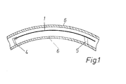
- the circuit board 1 is screwed onto the base 5 in the built-in housing 6 and with one end face 1a, on which there is an attachment 1b for locking, in the holder 4 fixedly arranged in the housing 6 is clamped, as a result of which the circuit board 1 is elastically bent and the contour of the housing 6 is adapted.
- the electronic components 2 arranged on the printed circuit board 1 are preferably aligned longitudinally in one direction parallel to a bending axis 3 shown in dashed lines and therefore stiffening of the printed circuit board 1 by the components 2 is avoided. Furthermore, the circuit board 1 is coated with (not shown) solder resist, so that these coated conductor tracks are not tinned and cracking during the bending process of the circuit board 1 is prevented.
Landscapes
- Engineering & Computer Science (AREA)
- Microelectronics & Electronic Packaging (AREA)
- Combinations Of Printed Boards (AREA)
- Telephone Set Structure (AREA)
- Structure Of Printed Boards (AREA)
- Devices For Indicating Variable Information By Combining Individual Elements (AREA)
Applications Claiming Priority (2)
| Application Number | Priority Date | Filing Date | Title |
|---|---|---|---|
| DE3119952 | 1981-05-20 | ||
| DE19813119952 DE3119952A1 (de) | 1981-05-20 | 1981-05-20 | Biegefreundliche leiterplatte mit zueinander parallel ausgerichteten bauelementen |
Publications (2)
| Publication Number | Publication Date |
|---|---|
| EP0065154A2 true EP0065154A2 (fr) | 1982-11-24 |
| EP0065154A3 EP0065154A3 (fr) | 1984-03-28 |
Family
ID=6132717
Family Applications (1)
| Application Number | Title | Priority Date | Filing Date |
|---|---|---|---|
| EP82103672A Withdrawn EP0065154A3 (fr) | 1981-05-20 | 1982-04-29 | Plaquette de circuit apte au cintrage |
Country Status (5)
| Country | Link |
|---|---|
| EP (1) | EP0065154A3 (fr) |
| AU (1) | AU552487B2 (fr) |
| DE (1) | DE3119952A1 (fr) |
| GB (1) | GB2098809B (fr) |
| SG (1) | SG66384G (fr) |
Cited By (2)
| Publication number | Priority date | Publication date | Assignee | Title |
|---|---|---|---|---|
| EP0199007A3 (fr) * | 1985-04-23 | 1988-07-27 | Bodenseewerk Gerätetechnik GmbH | Montage d'une plaque de circuit portant des éléments en cas d'une accélération forte |
| US9770571B2 (en) | 1996-10-16 | 2017-09-26 | Resmed Limited | Vent valve assembly |
Family Cites Families (3)
| Publication number | Priority date | Publication date | Assignee | Title |
|---|---|---|---|---|
| US3499220A (en) * | 1967-02-28 | 1970-03-10 | Amerace Esna Corp | Method of and apparatus for making a flexible,printed electrical circuit |
| US4136225A (en) * | 1977-07-08 | 1979-01-23 | Bell Telephone Laboratories, Incorporated | Cover coatings for printed circuits |
| GB1545531A (en) * | 1977-09-07 | 1979-05-10 | Gould Advance Ltd | Electronic assemblies |
-
1981
- 1981-05-20 DE DE19813119952 patent/DE3119952A1/de not_active Withdrawn
-
1982
- 1982-04-29 EP EP82103672A patent/EP0065154A3/fr not_active Withdrawn
- 1982-05-03 AU AU83223/82A patent/AU552487B2/en not_active Ceased
- 1982-05-13 GB GB8213932A patent/GB2098809B/en not_active Expired
-
1984
- 1984-09-18 SG SG66384A patent/SG66384G/en unknown
Cited By (2)
| Publication number | Priority date | Publication date | Assignee | Title |
|---|---|---|---|---|
| EP0199007A3 (fr) * | 1985-04-23 | 1988-07-27 | Bodenseewerk Gerätetechnik GmbH | Montage d'une plaque de circuit portant des éléments en cas d'une accélération forte |
| US9770571B2 (en) | 1996-10-16 | 2017-09-26 | Resmed Limited | Vent valve assembly |
Also Published As
| Publication number | Publication date |
|---|---|
| EP0065154A3 (fr) | 1984-03-28 |
| GB2098809B (en) | 1984-08-15 |
| AU8322382A (en) | 1982-11-25 |
| SG66384G (en) | 1985-03-15 |
| GB2098809A (en) | 1982-11-24 |
| DE3119952A1 (de) | 1982-12-09 |
| AU552487B2 (en) | 1986-06-05 |
Similar Documents
| Publication | Publication Date | Title |
|---|---|---|
| DE3790062C2 (fr) | ||
| DE3535923A1 (de) | Substrathaltender aufbau | |
| DE60128537T2 (de) | Zusammenbau zur verbindung von mindestens zwei gedruckten schaltungen | |
| DE1925791A1 (de) | Montagetafel fuer integrierte Schaltungen | |
| DE60003261T2 (de) | Elektrisches Verbindersystem für Flachkabel | |
| DE1791205B2 (de) | In einen Aufnahmerahmen eines Gerätes der elektrischen Nachrichtenoder Meßtechnik einschiebbare Baugruppe | |
| EP0065154A2 (fr) | Plaquette de circuit apte au cintrage | |
| DE3919273C2 (de) | Leiterplattenanordnung | |
| DE202015008007U1 (de) | Leiterplattenanordnung | |
| DE2948319C2 (de) | Verfahren zum Anbringen und Befestigen von Stromzuführungsdrähten an elektrischen Bauelementen | |
| DE1591581C3 (de) | Mikrowellen-Schattkreis in Triplate-Technik | |
| DE3329651C2 (fr) | ||
| DE29621580U1 (de) | Leitungs-Steckverbindung | |
| DE8114897U1 (de) | Biegefreundliche leiterplatte mit zueinander parallel ausgerichteten bauelementen | |
| DE3925157C2 (fr) | ||
| DE3316286A1 (de) | Vorrichtung zum kontaktieren von leiterplatten | |
| DE3211466C2 (de) | Leiterplattenanordnung | |
| DE10342047A1 (de) | Elektrisches Verbindungselement | |
| DE19613587C2 (de) | Anordnung zur Blockierung der elektromagnetischen Abstrahlung bei Leiterkarten und integrierten Schaltkreisen | |
| DE3133199C2 (de) | Kontaktsokel für elektrische Bauteile | |
| DE3046123C2 (de) | Steckverbinder zum Verbinden der Leiterbahnen von Leiterplatten | |
| DE4008542A1 (de) | Verfahren zum aendern von gedruckten leiterplatten | |
| DE7908303U1 (de) | Halter für Kühlbleche für elektronische Bauteile in einem Gerätechassis | |
| DE2652951A1 (de) | Schaltungsanordnung mit einer leiterplatte und darauf angeordneten bauelementen | |
| DE29514440U1 (de) | Leiterplatte für ein elektrisches oder elektronisches Gerät |
Legal Events
| Date | Code | Title | Description |
|---|---|---|---|
| PUAI | Public reference made under article 153(3) epc to a published international application that has entered the european phase |
Free format text: ORIGINAL CODE: 0009012 |
|
| AK | Designated contracting states |
Designated state(s): AT BE CH FR IT LU NL SE |
|
| PUAL | Search report despatched |
Free format text: ORIGINAL CODE: 0009013 |
|
| AK | Designated contracting states |
Designated state(s): AT BE CH FR IT LI LU NL SE |
|
| 17P | Request for examination filed |
Effective date: 19840330 |
|
| 17Q | First examination report despatched |
Effective date: 19860710 |
|
| RAP1 | Party data changed (applicant data changed or rights of an application transferred) |
Owner name: KRONE AKTIENGESELLSCHAFT |
|
| STAA | Information on the status of an ep patent application or granted ep patent |
Free format text: STATUS: THE APPLICATION HAS BEEN WITHDRAWN |
|
| 18W | Application withdrawn |
Withdrawal date: 19870121 |
|
| RIN1 | Information on inventor provided before grant (corrected) |
Inventor name: BECKER, PETER |