EP0065596B1 - Décodeur de signal - Google Patents
Décodeur de signal Download PDFInfo
- Publication number
- EP0065596B1 EP0065596B1 EP81109272A EP81109272A EP0065596B1 EP 0065596 B1 EP0065596 B1 EP 0065596B1 EP 81109272 A EP81109272 A EP 81109272A EP 81109272 A EP81109272 A EP 81109272A EP 0065596 B1 EP0065596 B1 EP 0065596B1
- Authority
- EP
- European Patent Office
- Prior art keywords
- whose
- input
- signal
- output
- switch
- Prior art date
- Legal status (The legal status is an assumption and is not a legal conclusion. Google has not performed a legal analysis and makes no representation as to the accuracy of the status listed.)
- Expired
Links
- 230000015654 memory Effects 0.000 description 16
- 230000005540 biological transmission Effects 0.000 description 2
- 230000006870 function Effects 0.000 description 1
- 238000003780 insertion Methods 0.000 description 1
- 230000037431 insertion Effects 0.000 description 1
- 238000000034 method Methods 0.000 description 1
Images



Classifications
-
- H—ELECTRICITY
- H04—ELECTRIC COMMUNICATION TECHNIQUE
- H04L—TRANSMISSION OF DIGITAL INFORMATION, e.g. TELEGRAPHIC COMMUNICATION
- H04L25/00—Baseband systems
- H04L25/38—Synchronous or start-stop systems, e.g. for Baudot code
- H04L25/40—Transmitting circuits; Receiving circuits
- H04L25/49—Transmitting circuits; Receiving circuits using code conversion at the transmitter; using predistortion; using insertion of idle bits for obtaining a desired frequency spectrum; using three or more amplitude levels ; Baseband coding techniques specific to data transmission systems
- H04L25/4917—Transmitting circuits; Receiving circuits using code conversion at the transmitter; using predistortion; using insertion of idle bits for obtaining a desired frequency spectrum; using three or more amplitude levels ; Baseband coding techniques specific to data transmission systems using multilevel codes
- H04L25/4923—Transmitting circuits; Receiving circuits using code conversion at the transmitter; using predistortion; using insertion of idle bits for obtaining a desired frequency spectrum; using three or more amplitude levels ; Baseband coding techniques specific to data transmission systems using multilevel codes using ternary codes
- H04L25/4925—Transmitting circuits; Receiving circuits using code conversion at the transmitter; using predistortion; using insertion of idle bits for obtaining a desired frequency spectrum; using three or more amplitude levels ; Baseband coding techniques specific to data transmission systems using multilevel codes using ternary codes using balanced bipolar ternary codes
Definitions
- the invention relates to a signal decoder for implementing a codirectional, divided into a positive and a negative half-wave and amplified
- 64 kbit / s interface signal in a binary information signal, in a 64 kHz clock and in an 8 kHz clock.
- Such interface signals are defined in the CCITT Orange Book, Vol. 111-2, Line Transmission, 1977, pages 432-433, G. 732 or page 458-459, G.744.
- Such a signal decoder is known from FR-A-2 407 617. This works with a monostable flip-flop whose analog tipping time fluctuates greatly as a result of component tolerances and temperature influences. This results in inadequate jitter tolerance, since the clock obtained can cause bit errors if the query is not timely.
- the invention is based on the object of realizing a signal decoder with better jitter tolerance.
- a first memory is provided for each half-wave, the input of which is connected via a first switch to the input for the half-wave
- a second memory is provided for each half-wave, whose input is connected to the output of a second switch, whose control input is in turn connected to the output of a controllable inverter, whose input is also connected to the input for the half-wave and whose control input is connected to the output of the first memory
- a third for each half-wave Memory is provided, the input of which is connected to the output of a third switch, the control input of which is in turn connected to the input for the half-wave
- a counter is provided for each half-wave, the start input of which is connected to the input for the first half-wave, the Stop entrance with the entrance for the second half wave is connected, the first command output is connected to the control input of the first switch, the second command output is connected to the input of the second switch and the third
- the decoded signal is derived exclusively from the edges of the input signal.
- the closing phase of the first switch is 3/8
- the closing phase of the second switch is 1/2
- the closing phase of the third switch is * 1 the duration of the code words for the states zero and one.
- the signal decoder according to the invention can advantageously be used in the data inputs of the PCM 30 F system, a PCM switch or a 64 kbit / s terminal.
- Fig. 1 shows the stages for forming the codirectional interface signal.
- Line a shows the bit number
- line b shows the states of the 64 kbit / s signal
- line c shows a signal in which the state zero by a code word "1010” and the state one by Code word "1100” is formed.
- Line d also shows a signal in which these code words are alternately reversed.
- Line e shows this signal in which every eighth code word violates the inversion rule. These places are marked with a V.
- Line f finally shows an 8 kHz Signal.
- FIG. 2 shows a signal decoder according to the invention.
- the arrangement contains an input 1, switches 2, 5 and 7, a controllable inverter 4, memories 3, 6 and 8 and a counter 9 for a half-wave.
- a corresponding arrangement for the other half-wave is identified with the same reference numerals but with an apostrophe.
- the outputs of the memories are combined by OR gates 10, 11 and 12.
- the counters 9 and 9 ' have a start input 14, 14', a stop input 15, 15 ', a first command output 16, 16', a second command output 17, 17 ', a third command output 18, 18' and a clock input 13.
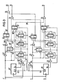
- Fig. 3 shows a practical embodiment of the signal decoder according to Fig. 2.
- the counter 9 consists of a divider (8: 1) 91, an inverter 92 and three stages 93, 94 and 95 of an internal counter.
- the RS memory 22, 22 ' forms the start / stop commands for both counters 9, 9'.
- the memory outputs are linked by gates 24, 25 and 26, which perform an OR function.
- the mode of operation of the signal decoder according to FIG. 3 can be tracked with the aid of the pulse plan in FIG. 4 using the circuit points listed.
Landscapes
- Physics & Mathematics (AREA)
- Spectroscopy & Molecular Physics (AREA)
- Engineering & Computer Science (AREA)
- Computer Networks & Wireless Communication (AREA)
- Signal Processing (AREA)
- Analogue/Digital Conversion (AREA)
- Synchronisation In Digital Transmission Systems (AREA)
- Dc Digital Transmission (AREA)
- Circuits Of Receivers In General (AREA)
- Selective Calling Equipment (AREA)
- Error Detection And Correction (AREA)
- Compression, Expansion, Code Conversion, And Decoders (AREA)
Claims (7)
Applications Claiming Priority (2)
| Application Number | Priority Date | Filing Date | Title |
|---|---|---|---|
| DE3120282 | 1981-05-21 | ||
| DE19813120282 DE3120282A1 (de) | 1981-05-21 | 1981-05-21 | Signaldecoder |
Publications (3)
| Publication Number | Publication Date |
|---|---|
| EP0065596A2 EP0065596A2 (fr) | 1982-12-01 |
| EP0065596A3 EP0065596A3 (en) | 1984-02-22 |
| EP0065596B1 true EP0065596B1 (fr) | 1986-02-26 |
Family
ID=6132915
Family Applications (1)
| Application Number | Title | Priority Date | Filing Date |
|---|---|---|---|
| EP81109272A Expired EP0065596B1 (fr) | 1981-05-21 | 1981-10-29 | Décodeur de signal |
Country Status (6)
| Country | Link |
|---|---|
| US (1) | US4473820A (fr) |
| EP (1) | EP0065596B1 (fr) |
| JP (1) | JPS57197946A (fr) |
| BR (1) | BR8202935A (fr) |
| DE (2) | DE3120282A1 (fr) |
| NO (1) | NO158979C (fr) |
Families Citing this family (2)
| Publication number | Priority date | Publication date | Assignee | Title |
|---|---|---|---|---|
| US5684833A (en) * | 1994-04-21 | 1997-11-04 | Aichidenshi Kabushiki Kaisha | Mutual conversion method of binary data and multilevel signal, its communication method, and its receiving device |
| DE10132048A1 (de) * | 2001-07-03 | 2003-01-23 | Siemens Ag | Ausgabeeinheit, Empfangseinheit, Anordnung zur Datenübertragung in einem Kraftfahrzeug sowie Verfahren dazu |
Family Cites Families (4)
| Publication number | Priority date | Publication date | Assignee | Title |
|---|---|---|---|---|
| US3787613A (en) * | 1972-06-27 | 1974-01-22 | Bell Telephone Labor Inc | Pulse transmission system for conveying data and control words by means of alternating polarity pulses and violations thereof |
| US3745361A (en) * | 1972-06-27 | 1973-07-10 | Bell Telephone Labor Inc | Composite clock signal generating and distributing circuits |
| FR2407617A1 (fr) * | 1977-10-28 | 1979-05-25 | Telecommunications Sa | Procede pour recevoir des jonctions codirectionnelles a 64 kbit/s et son dispositif de mise en oeuvre |
| US4380080A (en) * | 1980-12-30 | 1983-04-12 | Sperry Corporation | Tri-level differential line receiver |
-
1981
- 1981-05-21 DE DE19813120282 patent/DE3120282A1/de not_active Withdrawn
- 1981-10-29 EP EP81109272A patent/EP0065596B1/fr not_active Expired
- 1981-10-29 DE DE8181109272T patent/DE3173902D1/de not_active Expired
-
1982
- 1982-04-14 US US06/368,450 patent/US4473820A/en not_active Expired - Fee Related
- 1982-05-19 NO NO821664A patent/NO158979C/no unknown
- 1982-05-20 BR BR8202935A patent/BR8202935A/pt unknown
- 1982-05-20 JP JP57084132A patent/JPS57197946A/ja active Pending
Also Published As
| Publication number | Publication date |
|---|---|
| EP0065596A3 (en) | 1984-02-22 |
| NO158979C (no) | 1988-11-16 |
| EP0065596A2 (fr) | 1982-12-01 |
| JPS57197946A (en) | 1982-12-04 |
| NO158979B (no) | 1988-08-08 |
| US4473820A (en) | 1984-09-25 |
| DE3173902D1 (en) | 1986-04-03 |
| NO821664L (no) | 1982-11-22 |
| DE3120282A1 (de) | 1982-12-09 |
| BR8202935A (pt) | 1983-05-03 |
Similar Documents
| Publication | Publication Date | Title |
|---|---|---|
| DE2608902C3 (de) | Code-Wandler-Vorrichtung | |
| DE3544820A1 (de) | Taktfrequenzteilerschaltung | |
| CH620068A5 (fr) | ||
| DE3743586C2 (fr) | ||
| EP0065596B1 (fr) | Décodeur de signal | |
| DE3722907A1 (de) | Maximallaengen-schieberegister-folgegenerator | |
| EP0019821B1 (fr) | Procédé et dispositif pour la transmission d'une séquence binaire | |
| DE68922506T2 (de) | Frequenzteilerschaltung. | |
| DE2133660A1 (de) | Codierer | |
| DE1499930B2 (de) | Schaltung zur beseitigung der phasenverschiebung einzelner informationssignale gegenueber zahlreichen aufeinanderfolgenden, aus einer zweiphasenschrift abgeleiteten auslesesignalen | |
| EP0141946B1 (fr) | Dispositif pour la synchronisation des flancs de signaux binaires avec un signal d'horloge | |
| EP0198263A2 (fr) | Montage pour la transmission de signaux numériques sans mise à la terre par l'intermédiaire de points de séparation | |
| DE2143470A1 (de) | Codewandler | |
| DE1524122A1 (de) | Elektronische Datenverarbeitungsanlage mit Zeitaufteilung des Speicherzugriffs | |
| EP0326856A1 (fr) | Compteur électronique d'impulsions | |
| DE3042761C2 (de) | Schaltungsanordnung zur Gewinnung einer elektrischenBezugstakt-Impulsfolge für die Dekodierung einer von einem Aufzeichnungsträger gelesenen und auf diesem aufgezeichneten Mehrlängenschrift | |
| DE3324506C2 (fr) | ||
| DE3246211A1 (de) | Schaltungsanordnung zur detektion von folgen identischer binaerwerte | |
| DE2744942A1 (de) | Nachrichtenuebertragungssystem mit einer sende- und empfangseinrichtung | |
| DE2834798C3 (de) | Schaltungsanordnung zum Ansteuern einflankengesteuerter Bauelemente | |
| DE2443869A1 (de) | Digitaldatenuebertragungsanlage | |
| DE2603081C3 (de) | Schaltungsanordnung zur wahlweisen Verbindung mehrerer Eingänge mit mehreren Ausgängen | |
| DE3513694C2 (fr) | ||
| DE2605380B2 (de) | Schaltungsanordnung zum Erzeugen einer Rechteckschwingung aus der Mischung zweier Rechteckschwingungen miteinander | |
| DE2731482B1 (de) | Demultiplexer |
Legal Events
| Date | Code | Title | Description |
|---|---|---|---|
| PUAI | Public reference made under article 153(3) epc to a published international application that has entered the european phase |
Free format text: ORIGINAL CODE: 0009012 |
|
| 17P | Request for examination filed |
Effective date: 19811029 |
|
| AK | Designated contracting states |
Designated state(s): BE CH DE FR GB IT NL SE |
|
| PUAL | Search report despatched |
Free format text: ORIGINAL CODE: 0009013 |
|
| AK | Designated contracting states |
Designated state(s): BE CH DE FR GB IT LI NL SE |
|
| GRAA | (expected) grant |
Free format text: ORIGINAL CODE: 0009210 |
|
| AK | Designated contracting states |
Designated state(s): BE CH DE FR GB IT LI NL SE |
|
| PG25 | Lapsed in a contracting state [announced via postgrant information from national office to epo] |
Ref country code: BE Effective date: 19860226 |
|
| PG25 | Lapsed in a contracting state [announced via postgrant information from national office to epo] |
Ref country code: SE Effective date: 19860228 |
|
| REF | Corresponds to: |
Ref document number: 3173902 Country of ref document: DE Date of ref document: 19860403 |
|
| ITF | It: translation for a ep patent filed | ||
| ET | Fr: translation filed | ||
| PLBE | No opposition filed within time limit |
Free format text: ORIGINAL CODE: 0009261 |
|
| STAA | Information on the status of an ep patent application or granted ep patent |
Free format text: STATUS: NO OPPOSITION FILED WITHIN TIME LIMIT |
|
| 26N | No opposition filed | ||
| PGFP | Annual fee paid to national office [announced via postgrant information from national office to epo] |
Ref country code: GB Payment date: 19910913 Year of fee payment: 11 |
|
| PGFP | Annual fee paid to national office [announced via postgrant information from national office to epo] |
Ref country code: FR Payment date: 19911022 Year of fee payment: 11 |
|
| ITTA | It: last paid annual fee | ||
| PG25 | Lapsed in a contracting state [announced via postgrant information from national office to epo] |
Ref country code: GB Effective date: 19921029 |
|
| PGFP | Annual fee paid to national office [announced via postgrant information from national office to epo] |
Ref country code: NL Payment date: 19921031 Year of fee payment: 12 |
|
| PGFP | Annual fee paid to national office [announced via postgrant information from national office to epo] |
Ref country code: DE Payment date: 19921216 Year of fee payment: 12 |
|
| PGFP | Annual fee paid to national office [announced via postgrant information from national office to epo] |
Ref country code: CH Payment date: 19930121 Year of fee payment: 12 |
|
| GBPC | Gb: european patent ceased through non-payment of renewal fee |
Effective date: 19921029 |
|
| PG25 | Lapsed in a contracting state [announced via postgrant information from national office to epo] |
Ref country code: FR Effective date: 19930630 |
|
| REG | Reference to a national code |
Ref country code: FR Ref legal event code: ST |
|
| PG25 | Lapsed in a contracting state [announced via postgrant information from national office to epo] |
Ref country code: LI Effective date: 19931031 Ref country code: CH Effective date: 19931031 |
|
| PG25 | Lapsed in a contracting state [announced via postgrant information from national office to epo] |
Ref country code: NL Effective date: 19940501 |
|
| NLV4 | Nl: lapsed or anulled due to non-payment of the annual fee | ||
| REG | Reference to a national code |
Ref country code: CH Ref legal event code: PL |
|
| PG25 | Lapsed in a contracting state [announced via postgrant information from national office to epo] |
Ref country code: DE Effective date: 19940701 |