EP0065711A1 - Einrichtung mit einem in zweifacher Ausführung vorhandenen Taktgeber von hoher Funktionssicherheit - Google Patents
Einrichtung mit einem in zweifacher Ausführung vorhandenen Taktgeber von hoher Funktionssicherheit Download PDFInfo
- Publication number
- EP0065711A1 EP0065711A1 EP82104168A EP82104168A EP0065711A1 EP 0065711 A1 EP0065711 A1 EP 0065711A1 EP 82104168 A EP82104168 A EP 82104168A EP 82104168 A EP82104168 A EP 82104168A EP 0065711 A1 EP0065711 A1 EP 0065711A1
- Authority
- EP
- European Patent Office
- Prior art keywords
- circuit
- clock
- gate
- input
- filtering
- Prior art date
- Legal status (The legal status is an assumption and is not a legal conclusion. Google has not performed a legal analysis and makes no representation as to the accuracy of the status listed.)
- Granted
Links
Images



Classifications
-
- G—PHYSICS
- G06—COMPUTING OR CALCULATING; COUNTING
- G06F—ELECTRIC DIGITAL DATA PROCESSING
- G06F11/00—Error detection; Error correction; Monitoring
- G06F11/07—Responding to the occurrence of a fault, e.g. fault tolerance
- G06F11/16—Error detection or correction of the data by redundancy in hardware
- G06F11/1604—Error detection or correction of the data by redundancy in hardware where the fault affects the clock signals of a processing unit and the redundancy is at or within the level of clock signal generation hardware
-
- G—PHYSICS
- G04—HOROLOGY
- G04G—ELECTRONIC TIME-PIECES
- G04G3/00—Producing timing pulses
-
- G—PHYSICS
- G06—COMPUTING OR CALCULATING; COUNTING
- G06F—ELECTRIC DIGITAL DATA PROCESSING
- G06F1/00—Details not covered by groups G06F3/00 - G06F13/00 and G06F21/00
- G06F1/04—Generating or distributing clock signals or signals derived directly therefrom
-
- H—ELECTRICITY
- H04—ELECTRIC COMMUNICATION TECHNIQUE
- H04L—TRANSMISSION OF DIGITAL INFORMATION, e.g. TELEGRAPHIC COMMUNICATION
- H04L7/00—Arrangements for synchronising receiver with transmitter
- H04L7/0079—Receiver details
- H04L7/0083—Receiver details taking measures against momentary loss of synchronisation, e.g. inhibiting the synchronisation, using idle words or using redundant clocks
-
- G—PHYSICS
- G06—COMPUTING OR CALCULATING; COUNTING
- G06F—ELECTRIC DIGITAL DATA PROCESSING
- G06F11/00—Error detection; Error correction; Monitoring
- G06F11/07—Responding to the occurrence of a fault, e.g. fault tolerance
- G06F11/16—Error detection or correction of the data by redundancy in hardware
- G06F11/18—Error detection or correction of the data by redundancy in hardware using passive fault-masking of the redundant circuits
Definitions
- the invention relates to a device for increasing the operational safety of a duplicated clock.
- a duplicated clock is used for example in telecommunications centers to control a peripheral; it includes two clocks which each generate the time signals necessary to control the peripheral organs.
- each clock In the case of a telecommunications central office, each clock is generally controlled by three very reliable time bases, each time base delivering a clock signal and a synchronization signal. Each clock generally receives the three clock signals from the three time bases on a first majority circuit which delivers a majority signal from which it generates time signals which will be delivered to the peripheral, the majority clock signal can also be used. in the ring road to control certain organs.
- Each clock of a duplicated clock also receives, for example, the three synchronization signals from the three time bases on a second majority circuit which delivers a majority synchronization signal which is taken into account by the majority clock signal.
- the majority clock signal is generally filtered and reshaped in a filtering and shaping circuit before being used for the elaboration of the time signals and for taking into account the majority synchronization signal.
- a clock of a duplicated clock is connected to a part of the organs of the peripheral, the other clock being connected to another part of the organs of the same peripheral.
- the clock signals obtained at the output of the filtering and shaping circuit of each clock can be phase shifted; this phase difference is found between the time signals delivered by each clock which can adversely affect the proper functioning the device and put it out of service when this phase shift is too great.
- the object of the present invention is to increase the operating safety of a duplicated clock and thus to reduce the causes of the deactivation of a peripheral, and in general of the device to which it delivers the time signals.
- FIG. 1 represents a duplicated clock made up of two clocks 1 and 2.
- Each clock comprises a first majority circuit 3 receiving clock signals h1, h2, h3 from three time bases, and a second majority circuit 5 receiving signals from synchronization Sy1, Sy2, Sy3 of the three time bases.
- the first majority circuit 3 delivers a majority clock signal to a filtering and shaping circuit 4 which delivers a reconstructed clock signal w1 for the clock 1 and w2 for the clock 2.
- a circuit of choice 6 receives, in each clock, the reconstructed clock signals w1 and w2, and outputs a clock signal w.
- a unitary register 7 receives a majority synchronization signal from the second majority circuit 5, and is controlled by the clock signal w; it delivers a synchronization signal Sy.
- a time signal processing circuit 8 receives the clock signal w; it works out by dividing the clock signal w, different time signals t1 to tn.
- Each choice circuit 6 comprises a first processing circuit 11, a second processing circuit 12 and an output circuit 13.
- the first and second processing circuits receive the reconstituted clock signals w1 and w2; the first processing circuit 11 is controlled by the reconstructed clock signal w2 and the second processing circuit 12 is controlled by the reconstructed clock signal w1.
- the device for increasing the operating safety of a duplicated clock is therefore constituted by the two choice circuits 6 each located in a clock.
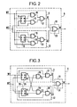
- FIG. 2 illustrates a first embodiment of the choice circuit 6 of FIG. 1.
- the first processing circuit 11 comprises a flip-flop 14 of type D for example, and three AND-NON (NAND) gates 15, 16, 17.
- the flip-flop 14 receives the reconstituted clock signal w1 on its signal input D, and the reconstituted clock signal w2 on its clock input; its direct output Q1 is connected to an input of the AND-NO gate 15, another input of which receives the reconstructed clock signal w1; its reverse output Q1 is connected to an input of the AND-NON gate 16 which receives on another input the reconstructed clock signal w2.
- the AND-NO gate 17 has an input connected to the output of the AND-NO gate 15 and another input connected to the output of the AND-NO gate 16.
- the second processing circuit 12 is identical to the first processing circuit 11. It therefore comprises a flip-flop 18 and three AND-NO gates 19, 20, 21.
- the flip-flop 18 receives the reconstructed clock signal w2 on its signal input D and the reconstructed clock signal w1 on its clock input; its direct output Q2 is connected to an input of the AND-NON gate 19 of which another input receives the reconstituted clock signal w2, and its reverse output Q2 is connected to an input of the AND-NON gate which receives on a other input the reconstructed clock signal w1.
- the AND-NO gate 21 has an input connected to the output of the AND-NO gate 19 and another input connected to the output of the AND-NO gate 20.
- the output circuit 13 is formed. by an OR gate 22 having an input connected to the output of the AND-NO gate 17 of the first processing circuit 11, and another input connected to the output of the AND-NO gate 21 of the second processing circuit 12.
- the gate OR 22 delivers the clock signal w.
- FIG. 3 illustrates a second embodiment of the choice circuit 6 of FIG. 1.
- the first processing circuit 11 comprises a flip-flop 25, of type D for example, and two AND-NON gates 26, 27;
- the second processing circuit 12 is identical to the first processing circuit 11 and comprises a flip-flop 28 and two AND-NO gates 29, 30;
- the output circuit 13 is constituted by an AND-NO gate 31.
- the flip-flop 25 receives the reconstructed clock signal w1 on its signal input D and the reconstructed clock signal w2 on its clock input; its output Q1 is connected to an input of the AND-NON gate 29 of the second processing circuit, and its output Q1 is connected to an input of the AND-NON gate 26.
- the flip-flop 28 receives the reconstructed clock signal w2 on its signal input D and the reconstituted clock signal w1 on its clock input; its output Q2 is connected to an input of the AND-NO gate 26 of the first of the first processing circuit 11, its output Q2 being connected to an input of the AND-NO gate 29.
- the output of the AND-NO gate 26 is connected to an input of the AND-NO gate 27, another input of which receives the reconstructed clock signal w1;
- the output of the AND-NO gate 29 is connected to an input of the AND-NO gate 30, another input of which receives the reconstructed clock signal w2.
- the AND-NO gate 31 of the output circuit 13 has an input connected to the output of the AND-NO gate 27 and another input connected to the output of the AND-NO gate 30; its output delivers the clock signal w.
- Figure 4 is a timing diagram which represents the different signals in the choice circuit.
- w1 and w2 having the value 0
- q1 o
- q2 o
- w1 goes to 1
- the reconstituted clock signals w1 and w2 being established and w1 being ahead of w2, the various signals of the choice circuit no longer change in value, except A1 which takes the value 1 when w1 goes to o, and the value o when w1 goes to 1.
- the clock signal w therefore alternately goes to o and to 1 at the rate of w1.
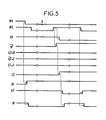
- FIG. 5- is a timing diagram which represents the various signals in the choice circuit, the reference X indicating the appearance of the fault on w1.
- FIG. 6 is a timing diagram which represents the different signals in the choice circuit.
- the clock signal w delivered by each choice circuit therefore corresponds to w1 if w1 is ahead of w2, to w2 if w2 is ahead of w1, and to w2 if w1 is down.
- w2 breaks down when w1 is ahead of w2
- FIG. 4 shows that when in steady state, signal A2 remains at 1 that whatever the value of w2; a breakdown on w2 therefore does not change the established regime. It would be the same if w1 broke down when w2 was ahead of w1.
Landscapes
- Engineering & Computer Science (AREA)
- Theoretical Computer Science (AREA)
- Physics & Mathematics (AREA)
- General Physics & Mathematics (AREA)
- General Engineering & Computer Science (AREA)
- Quality & Reliability (AREA)
- Computer Networks & Wireless Communication (AREA)
- Signal Processing (AREA)
- Synchronisation In Digital Transmission Systems (AREA)
- Hardware Redundancy (AREA)
- Electric Clocks (AREA)
- Detection And Prevention Of Errors In Transmission (AREA)
Applications Claiming Priority (2)
| Application Number | Priority Date | Filing Date | Title |
|---|---|---|---|
| FR8110022 | 1981-05-20 | ||
| FR8110022A FR2506478A1 (fr) | 1981-05-20 | 1981-05-20 | Dispositif pour augmenter la securite de fonctionnement d'une horloge dupliquee |
Publications (2)
| Publication Number | Publication Date |
|---|---|
| EP0065711A1 true EP0065711A1 (de) | 1982-12-01 |
| EP0065711B1 EP0065711B1 (de) | 1984-09-19 |
Family
ID=9258678
Family Applications (1)
| Application Number | Title | Priority Date | Filing Date |
|---|---|---|---|
| EP82104168A Expired EP0065711B1 (de) | 1981-05-20 | 1982-05-13 | Einrichtung mit einem in zweifacher Ausführung vorhandenen Taktgeber von hoher Funktionssicherheit |
Country Status (8)
| Country | Link |
|---|---|
| US (1) | US4480198A (de) |
| EP (1) | EP0065711B1 (de) |
| JP (1) | JPS5837586A (de) |
| DE (1) | DE3260773D1 (de) |
| ES (1) | ES8304678A1 (de) |
| FR (1) | FR2506478A1 (de) |
| IE (1) | IE52991B1 (de) |
| PT (1) | PT74932A (de) |
Cited By (2)
| Publication number | Priority date | Publication date | Assignee | Title |
|---|---|---|---|---|
| EP0162870A4 (de) * | 1983-11-07 | 1988-04-26 | Motorola Inc | Mikrorechner mit synthesiertem taktgenerator und leistungseinsparung. |
| EP0280258A3 (en) * | 1987-02-25 | 1990-05-02 | Stratus Computer, Inc. | Fault-tolerant digital timing apparatus and method |
Families Citing this family (16)
| Publication number | Priority date | Publication date | Assignee | Title |
|---|---|---|---|---|
| NL8202685A (nl) * | 1982-07-05 | 1984-02-01 | Philips Nv | Kloksignaalregenerator met hoge stabiliteit. |
| US4644498A (en) * | 1983-04-04 | 1987-02-17 | General Electric Company | Fault-tolerant real time clock |
| US4696019A (en) * | 1984-09-19 | 1987-09-22 | United Technologies Corporation | Multi-channel clock synchronizer |
| FR2577087B1 (fr) * | 1985-02-07 | 1987-03-06 | Thomson Csf Mat Tel | Dispositif de distribution d'horloge tripliquee, chaque signal d'horloge comportant un signal de synchronisation |
| US4644568A (en) * | 1985-03-28 | 1987-02-17 | At&T Bell Laboratories | Timing signal distribution arrangement |
| GB8615399D0 (en) * | 1986-06-24 | 1986-07-30 | Int Computers Ltd | Switching circuit |
| US4882738A (en) * | 1987-06-25 | 1989-11-21 | Nec Corporation | Clock control system |
| US4922489A (en) * | 1987-10-23 | 1990-05-01 | Siemens Aktiengesellschaft | Circuit configuration for routine testing of the clock supply of a large number of units operated with the same clock |
| NL8800872A (nl) * | 1988-04-06 | 1989-11-01 | Philips Nv | Geintegreerde schakeling. |
| DE3905689A1 (de) * | 1989-02-24 | 1990-08-30 | Philips Patentverwaltung | Schaltungsanordnung mit zwei parallelen zweigen zur uebertragung eines binaersignales |
| US4979191A (en) * | 1989-05-17 | 1990-12-18 | The Boeing Company | Autonomous N-modular redundant fault tolerant clock system |
| US5123107A (en) * | 1989-06-20 | 1992-06-16 | Mensch Jr William D | Topography of CMOS microcomputer integrated circuit chip including core processor and memory, priority, and I/O interface circuitry coupled thereto |
| US5175734A (en) * | 1989-09-27 | 1992-12-29 | Siemens Aktiengesellschaft | Clock supply for multiplex systems |
| US5377205A (en) * | 1993-04-15 | 1994-12-27 | The Boeing Company | Fault tolerant clock with synchronized reset |
| US6718474B1 (en) | 2000-09-21 | 2004-04-06 | Stratus Technologies Bermuda Ltd. | Methods and apparatus for clock management based on environmental conditions |
| US6404240B1 (en) * | 2000-10-30 | 2002-06-11 | Semiconductor Components Industries Llc | Circuit and method of a three state phase frequency lock detector |
Citations (4)
| Publication number | Priority date | Publication date | Assignee | Title |
|---|---|---|---|---|
| DE2157982A1 (de) * | 1971-03-10 | 1972-09-14 | Ibm | Digitales Multiprozessor-Datenverarbeitungssystem |
| FR2315736A1 (fr) * | 1975-06-25 | 1977-01-21 | Materiel Telephonique | Systeme de transmission de signaux periodiques |
| US4185245A (en) * | 1978-05-15 | 1980-01-22 | International Telephone And Telegraph Corporation | Fault-tolerant clock signal distribution arrangement |
| FR2433878A1 (fr) * | 1978-08-18 | 1980-03-14 | Labo Cent Telecommunicat | Circuit d'horloge pour ensemble electronique |
Family Cites Families (2)
| Publication number | Priority date | Publication date | Assignee | Title |
|---|---|---|---|---|
| SE326321B (de) * | 1968-11-15 | 1970-07-20 | E Sjoequist | |
| GB1603647A (en) * | 1977-04-29 | 1981-11-25 | Bourner M | Pulse order recognition circuit |
-
1981
- 1981-05-20 FR FR8110022A patent/FR2506478A1/fr active Pending
-
1982
- 1982-05-12 JP JP57079806A patent/JPS5837586A/ja active Pending
- 1982-05-13 DE DE8282104168T patent/DE3260773D1/de not_active Expired
- 1982-05-13 EP EP82104168A patent/EP0065711B1/de not_active Expired
- 1982-05-19 PT PT74932A patent/PT74932A/pt unknown
- 1982-05-19 ES ES512362A patent/ES8304678A1/es not_active Expired
- 1982-05-19 IE IE1200/82A patent/IE52991B1/en unknown
- 1982-05-20 US US06/380,313 patent/US4480198A/en not_active Expired - Fee Related
Patent Citations (4)
| Publication number | Priority date | Publication date | Assignee | Title |
|---|---|---|---|---|
| DE2157982A1 (de) * | 1971-03-10 | 1972-09-14 | Ibm | Digitales Multiprozessor-Datenverarbeitungssystem |
| FR2315736A1 (fr) * | 1975-06-25 | 1977-01-21 | Materiel Telephonique | Systeme de transmission de signaux periodiques |
| US4185245A (en) * | 1978-05-15 | 1980-01-22 | International Telephone And Telegraph Corporation | Fault-tolerant clock signal distribution arrangement |
| FR2433878A1 (fr) * | 1978-08-18 | 1980-03-14 | Labo Cent Telecommunicat | Circuit d'horloge pour ensemble electronique |
Non-Patent Citations (1)
| Title |
|---|
| IEEE COMPUTER SOCIETY, THE NINTH ANNUAL INTERNATIONAL SYMPOSIUM ON FAULT-TOLERANT COMPUTING, 20-22 juin 1979, pages 33-39, Madison, Wisconsin; F.T.C.S.-9, IEEE catalog no. 79CH1396-IC * |
Cited By (2)
| Publication number | Priority date | Publication date | Assignee | Title |
|---|---|---|---|---|
| EP0162870A4 (de) * | 1983-11-07 | 1988-04-26 | Motorola Inc | Mikrorechner mit synthesiertem taktgenerator und leistungseinsparung. |
| EP0280258A3 (en) * | 1987-02-25 | 1990-05-02 | Stratus Computer, Inc. | Fault-tolerant digital timing apparatus and method |
Also Published As
| Publication number | Publication date |
|---|---|
| ES512362A0 (es) | 1983-03-01 |
| EP0065711B1 (de) | 1984-09-19 |
| ES8304678A1 (es) | 1983-03-01 |
| IE821200L (en) | 1982-11-20 |
| IE52991B1 (en) | 1988-04-27 |
| JPS5837586A (ja) | 1983-03-04 |
| PT74932A (fr) | 1982-06-01 |
| DE3260773D1 (en) | 1984-10-25 |
| US4480198A (en) | 1984-10-30 |
| FR2506478A1 (fr) | 1982-11-26 |
Similar Documents
| Publication | Publication Date | Title |
|---|---|---|
| EP0065711B1 (de) | Einrichtung mit einem in zweifacher Ausführung vorhandenen Taktgeber von hoher Funktionssicherheit | |
| FR2371017A1 (fr) | Systeme de traitement d'entree/sortie utilisant des processeurs verrouilles | |
| KR950033826A (ko) | 소형컴퓨터 인터페이스 시스템상의 신호로부터 노이즈를 제거하는 이중필터링 글리치 제거기 | |
| FR2488079A1 (fr) | Dispositif de filtrage numerique | |
| FR2480968A1 (fr) | Processeur numerique adapte a l'integration a haute densite | |
| US20050018796A1 (en) | Method of combining an analysis filter bank following a synthesis filter bank and structure therefor | |
| EP0452878B1 (de) | Multiplexierungsanordnung für Taktsignale | |
| EP0298569B1 (de) | Gerät zum Ausschliessen von Festechos für Ultraschallechographie | |
| FR2739991A1 (fr) | Dispositif de filtrage numerique | |
| CA2284899A1 (fr) | Filtre numerique pour retards fractionnaires | |
| CA2106703A1 (fr) | Procede pour determiner la transmittance d'un circuit de filtrage prevu pour transformer la reponse impulsionnelle d'un filtre en une reponse a phase minimale et filtre mettant enoeuvre ce procede | |
| US6501406B1 (en) | Digital filter | |
| FR2476935A1 (fr) | Procede de reglage de la phase de l'horloge d'un systeme de reception de donnees numeriques, circuit de recuperation de phase pour la mise en oeuvre de ce procede, et systeme de reception de donnees numeriques comprenant ce circuit. | |
| FR2646918A1 (fr) | Dispositif de mesure de la vitesse d'ecoulements sanguins par echographie ultrasonore a cadence de mesure amelioree | |
| KR960040319A (ko) | 초음파칼라도플러영상시스템의 클러터신호 필터링방법 | |
| FR2394933A1 (fr) | Filtre numerique en treillis pour la synthese de signaux ou de la parole | |
| CA1126867A (fr) | Dispositif de controle de la qualite d'un signal de transmission numerique synchrone | |
| KR910002248A (ko) | 디지탈 신호 노이즈 삭제 방법 및 그 장치 | |
| EP0115737A1 (de) | Matrix-Umsetzungssystem für ein Videosystem mit einem dynamisch definierbaren Zeichensatz | |
| JPH1132031A (ja) | クロック再生装置 | |
| EP3745234A1 (de) | Vorrichtung mit mehreren taktbereichen | |
| FR2415399A1 (fr) | Circuit de traitement de signaux pour appareil de prise de vue de television couleur | |
| JPS6010913A (ja) | パルス信号のノイズ除去回路 | |
| FR2642919A1 (fr) | Circuit de logique combinatoire rapide | |
| FR2504766A1 (fr) | Circuit de separation des signaux de luminance et de chrominance et recepteur de television comportant un tel circuit |
Legal Events
| Date | Code | Title | Description |
|---|---|---|---|
| PUAI | Public reference made under article 153(3) epc to a published international application that has entered the european phase |
Free format text: ORIGINAL CODE: 0009012 |
|
| AK | Designated contracting states |
Designated state(s): BE DE FR GB IT |
|
| 17P | Request for examination filed |
Effective date: 19830526 |
|
| ITF | It: translation for a ep patent filed | ||
| GRAA | (expected) grant |
Free format text: ORIGINAL CODE: 0009210 |
|
| AK | Designated contracting states |
Designated state(s): BE DE FR GB IT |
|
| REF | Corresponds to: |
Ref document number: 3260773 Country of ref document: DE Date of ref document: 19841025 |
|
| PLBE | No opposition filed within time limit |
Free format text: ORIGINAL CODE: 0009261 |
|
| STAA | Information on the status of an ep patent application or granted ep patent |
Free format text: STATUS: NO OPPOSITION FILED WITHIN TIME LIMIT |
|
| 26N | No opposition filed | ||
| PGFP | Annual fee paid to national office [announced via postgrant information from national office to epo] |
Ref country code: GB Payment date: 19900418 Year of fee payment: 9 |
|
| PGFP | Annual fee paid to national office [announced via postgrant information from national office to epo] |
Ref country code: FR Payment date: 19900523 Year of fee payment: 9 |
|
| ITTA | It: last paid annual fee | ||
| PGFP | Annual fee paid to national office [announced via postgrant information from national office to epo] |
Ref country code: BE Payment date: 19900613 Year of fee payment: 9 |
|
| PGFP | Annual fee paid to national office [announced via postgrant information from national office to epo] |
Ref country code: DE Payment date: 19900626 Year of fee payment: 9 |
|
| PG25 | Lapsed in a contracting state [announced via postgrant information from national office to epo] |
Ref country code: GB Effective date: 19910513 |
|
| PG25 | Lapsed in a contracting state [announced via postgrant information from national office to epo] |
Ref country code: BE Effective date: 19910531 |
|
| BERE | Be: lapsed |
Owner name: LA TELEPHONIE INDUSTRIELLE ET COMMERCIALE TELIC A Effective date: 19910531 |
|
| GBPC | Gb: european patent ceased through non-payment of renewal fee | ||
| PG25 | Lapsed in a contracting state [announced via postgrant information from national office to epo] |
Ref country code: FR Effective date: 19920131 |
|
| PG25 | Lapsed in a contracting state [announced via postgrant information from national office to epo] |
Ref country code: DE Effective date: 19920303 |
|
| REG | Reference to a national code |
Ref country code: FR Ref legal event code: ST |