EP0115737A1 - Matrix-Umsetzungssystem für ein Videosystem mit einem dynamisch definierbaren Zeichensatz - Google Patents
Matrix-Umsetzungssystem für ein Videosystem mit einem dynamisch definierbaren Zeichensatz Download PDFInfo
- Publication number
- EP0115737A1 EP0115737A1 EP83460006A EP83460006A EP0115737A1 EP 0115737 A1 EP0115737 A1 EP 0115737A1 EP 83460006 A EP83460006 A EP 83460006A EP 83460006 A EP83460006 A EP 83460006A EP 0115737 A1 EP0115737 A1 EP 0115737A1
- Authority
- EP
- European Patent Office
- Prior art keywords
- pixels
- phase
- inputs
- outputs
- transformed
- Prior art date
- Legal status (The legal status is an assumption and is not a legal conclusion. Google has not performed a legal analysis and makes no representation as to the accuracy of the status listed.)
- Granted
Links
- 239000011159 matrix material Substances 0.000 title claims abstract description 32
- 238000006243 chemical reaction Methods 0.000 title claims abstract description 12
- 238000011144 upstream manufacturing Methods 0.000 claims description 8
- 230000000717 retained effect Effects 0.000 claims 1
- 238000010586 diagram Methods 0.000 description 13
- 230000015654 memory Effects 0.000 description 3
- 230000004913 activation Effects 0.000 description 2
- 235000021183 entrée Nutrition 0.000 description 2
- 230000006870 function Effects 0.000 description 2
- 230000001960 triggered effect Effects 0.000 description 2
- 241000287107 Passer Species 0.000 description 1
- 238000004458 analytical method Methods 0.000 description 1
- 238000000034 method Methods 0.000 description 1
- 101150093826 par1 gene Proteins 0.000 description 1
- 230000001502 supplementing effect Effects 0.000 description 1
- 230000009466 transformation Effects 0.000 description 1
Images




Classifications
-
- G—PHYSICS
- G09—EDUCATION; CRYPTOGRAPHY; DISPLAY; ADVERTISING; SEALS
- G09G—ARRANGEMENTS OR CIRCUITS FOR CONTROL OF INDICATING DEVICES USING STATIC MEANS TO PRESENT VARIABLE INFORMATION
- G09G5/00—Control arrangements or circuits for visual indicators common to cathode-ray tube indicators and other visual indicators
- G09G5/22—Control arrangements or circuits for visual indicators common to cathode-ray tube indicators and other visual indicators characterised by the display of characters or indicia using display control signals derived from coded signals representing the characters or indicia, e.g. with a character-code memory
- G09G5/24—Generation of individual character patterns
- G09G5/26—Generation of individual character patterns for modifying the character dimensions, e.g. double width, double height
Definitions
- the present invention relates to a transcoding system between elementary matrices to 12x10 dots and 8x10 points, respectively in matrices videography systems and dynamic alphabets q uement redefinable.
- Known matrix or alpha-mosaic graphics videography systems are, for example, the French Teletel and Antiope systems or the British Prestel and Ceefax systems.
- the Canadian Telidon system is a system with alphageometric graphics which is not concerned with the present invention.
- An object of the present invention is to provide a transcoding system which provides low distortions and which can be implemented by simple means which do not significantly increase the cost of the terminal.
- the logical processing of a group of three initial pixels a, b, c produces a group of transformed pixels â, b, according to the following logical formulas:
- the pixels b and â ', calculated in the second phase are defined, either by the following two logical equations: and either by the two equivalent logical equations (I '). and (II ') where - is replaced by +.
- a conversion circuit operating according to the system of the invention and comprising an input of digital signals of matrix 12 ⁇ 10 connected to the input of a set of three upstream shift registers with twelve cells, mounted in series, the outputs of the first and second upstream registers being connected to the corresponding inputs of a first phase calculation circuit, a digital signal output of matrix 8 ⁇ 10 connected to the output of a set of three downstream registers with eight stages, connected in series, the outputs of the first phase calculation circuit being connected to the parallel inputs of the first downstream register, the parallel outputs of the second upstream register being connected to corresponding inputs of a second phase processing circuit, the parallel outputs of the first and third upstream registers being connected by an inverter circuit to corresponding inputs of the second phase processing circuit, the parallel outputs, except the first and the last, of the third downstream register being connected to corresponding inputs of the second phase processing circuit, the outputs of the second phase processing circuit being connected to the parallel inputs, except the first and the last, of the second phase processing circuit, the outputs
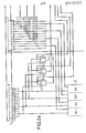
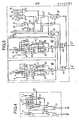
- Fig. 1 is a relatively simplified block diagram showing the entire 12/8 converter.
- the input wires of the transcoding circuit of FIG. 1 include the wires 1, 2 and 3 corresponding respectively to the wires 85, 84 and 83 mentioned above, and the output wires 4, 5, and 6 connected to a random access memory of character 7, corresponding to 37.
- Wire 3 is connected to the input of a shift register 73 which is intended to delay the character address by a time equivalent to the processing of the first three lines of the character.
- the synchronization of the register 73 is carried out by the signal presented on the wire 5 coming from the control logic 12.
- Wire 2 is connected to the input of a shift register 72 which is intended to delay each line address received by a processing time equivalent to the processing time of three character lines.
- the synchronization of the register 72 is carried out by the signal presented on the wire 6 coming from the control logic 12.
- Wire 1 is connected to the data input of a shift register 8, the serial output of which is connected to the data input of a shift register 9.
- the serial output of shift register 9 is connected to l input of a shift register 10.
- the three shift registers 8, 9 and 10 each have twelve stages and can therefore each store a matrix line. Their clock inputs are connected to the output 11 of a clock circuit 12.
- the registers 8 to 10 can be circuits of the type sold under the reference DM 74 195.
- Register 8 has its parallel outputs "1", “2” and “3” connected to the corresponding inputs of a first logic processing circuit 13.1, its parallel outputs “4", “5" and “6” connected to the corresponding inputs of a second logic processing circuit 13.2, its outputs “7”, “8” and “9” connected to the corresponding inputs of a third logic processing circuit 13.3, and its parallel outputs "10", “11” and “ 12 “connected to the corresponding inputs of a fourth logic processing circuit 13.4. All of the circuits 13.1, 13.2, 13.3 and 13.4, which are identical, form a circuit of conversion 13 which converts slices of three pixels into slices of two pixels.
- the register 9 has its parallel outputs "1", “2” and “3” connected to corresponding inputs of the circuit 13.1, its parallel outputs "4", “5" and “6” connected to corresponding inputs of circuit 13.2, its parallel outputs "7”, “8” and “9” connected to corresponding inputs of circuit 13.3, and its parallel outputs " 1 0 " , " 11" and "12” connected to inputs 13.4.
- the circuit 13.1 has two outputs which are respectively connected to the parallel inputs "1" and "2" of an eight-stage shift register 14; the circuit 13.2 has two outputs respectively connected to the parallel inputs "3" and "4" of the register 14; the circuit 13.3 has two outputs connected respectively to the parallel inputs "5" and "6” of the register 14; and the circuit 13.4 has two outputs respectively connected to the inputs "7" and "8" of the register 14.
- the serial output of the register 14 is connected to the input of a shift register 15 with eight stages.
- the serial output of register 15 is connected to the serial input of another shift register 16 with eight stages, the output of which is connected to wire 4.
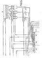
- the register 8 also has its parallel outputs "1" to "3" connected respectively to the first inputs of three doors AND P1; its parallel outputs "4" to “6” connected respectively, on the one hand, to the first inputs of three AND gates Q1 and, on the other hand, to the first inputs of three AND gates P2; its three parallel outputs "7” to “9” connected respectively, on the one hand, to the first inputs of three AND gates Q2 and, on the other hand, to the first inputs of three AND gates P3; and, finally, its three parallel outputs "10” to "12” connected to the first inputs of three AND gates Q3.
- the set of AND gates P1 to P3 and Q1 to Q3 form a switch 17.
- the outputs of AND gates P1 and Q1 are respectively connected to the first inputs of six OR gates R1; the outputs of AND gates P2 and Q2 are respectively connected to the first inputs of six OR gates R2, and the outputs of AND gates P3 and Q3 are respectively connected to the first inputs of six OR gates R3.
- the OR gates R1 to R3 form the connection circuit 18.
- the outputs of the six OR gates Rl are connected to the corresponding inputs A1 to A6 of a circuit logical processing 19.1; the outputs of the six OR gates R2 are connected to the corresponding inputs A of a logic processing circuit 19.2, and the outputs of the six OR gates R3 are connected to the corresponding inputs A of a third logic processing circuit 19.3.
- the circuit 19.1 has two outputs which are respectively connected to the parallel inputs "2" and "3" of the register 15; circuit 19.2 has two outputs which are respectively connected to inputs "4" and "5" of register 15; and the circuit 19.3 has two outputs which are respectively connected to the inputs "6" and "7" of the register 15.
- circuit 19.1 has inputs B which are respectively connected to the parallel outputs "2", “3", "4" and "5" of the register 9; circuit 19.2 has inputs B which are respectively connected to parallel outputs "5", "6", "7" and "8" of register 9; and circuit 19.3 has inputs B which are respectively connected to outputs "8", "9", "10" and "11" of register 9.
- the circuit 19.1 also has inputs C which are respectively connected to the parallel outputs "2" and "3" of the register 16; the circuit 19.2 has inputs C which are respectively connected to the parallel outputs "4" and "5" of the register 16; and the circuit 19.3 has inputs C which are respectively connected to the parallel outputs "6" and "7" of the register 16.
- circuit 19.1 has an output D connected to the second inputs of the doors Pl and Q1; circuit 19.2 has an output D connected to the second inputs of AND gates P2 and Q2; and circuit 19.3 has an output D connected to the second inputs of AND gates P3 and Q3.
- the register 10 has its parallel outputs "1" to "3" connected respectively to the first inputs of three doors AND P'l; its parallel outputs "4" to “6” connected respectively, on the one hand, to the first inputs of three AND gates Q'l and, on the other hand, to the first inputs of three AND gates P'2; its three parallel outputs "7” to “9” connected respectively, on the one hand, to the first inputs of three AND gates Q'2 and, on the other hand, to the first inputs of three AND gates P'3; and, finally, its three parallel outputs "10" to "12” connected to the first inputs of three AND gates Q3.
- the set of AND gates P'1 to P'3 and Q'1 to Q'3 form a commuta 20.
- AND gates P'1 and Q '] are respectively connected to the second inputs of the six OR gates R1; the outputs of AND gates P'2 and Q'2 are respectively connected to the second inputs of the six OR gates R2, and the outputs of AND gates P'3 and Q'3 are respectively connected to the second inputs of the six OR R3 gates.
- the circuit 19.1 has an output E connected to the second inputs of the doors P'1 and Q'l; circuit 19.2 has an output E connected to the second inputs of AND gates P'2 and Q'2; and the circuit 19.3 has an output E connected to the second inputs of the AND gates P'3 and Q'3.
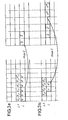
- FIG. 3a Before describing in detail the logic processing circuit 13.1, FIG. 4, and the logic processing circuit 19.1, FIG. 5, we will consider the diagrams of Figs. 3a and 3b.
- FIG. 3a In the diagram of FIG. 3a, there is shown on the left, looking at the drawing, a portion of matrix 12 ⁇ 10 and, on the right, the transformed portion of matrix 8 ⁇ 10, after passing through the circuit 13.1.
- This transformation will hereinafter be designated by first phase or phase 1.
- the twelve pixels of a line i are grouped into four groups of three pixels: a, b, c; a ', b', c '; a ", b", etc.
- Each group of three pixels is transformed into a group of two pixels in the 8x10 matrix.
- Each line of the 8x10 matrix comprises four groups of transformed pixels: â, b ⁇ , â ', b'; â ", etc. More particularly, for the matrix 12x10, there is shown, at line i, a first group of three pixels a, b, c, followed by a second group of three pixels a ', b', c ', and, at line (i-1), the first corresponding group of three pixels a- 1, b- 1, c- 1, followed by the second corresponding group of three pixels a'-1, b' -1 , c ' -1 , corresponding to them, in the 8x10 matrix, at line i, the first group of two pixels â, b, followed by the second group of two pixels â', b ⁇ '.
- Fig. 4 shows in detail the logic diagram of the logic processing circuit 13.1 which calculates the pixels a and b as a function of the pixels a, b, c, a -1 , b- 1 and c- 1 , according to the following logic equations:
- the digital references of the inputs are those of the pixel data to which they correspond.
- Input a is connected, on the one hand, to the inverting input of an AND gate 21 and, on the other hand, to the input of an OR gate 22.
- Input b is connected to the non-inverting input of AND gate 21.
- Input c is connected, on the one hand, to the other inverting input of AND gate 21 and, on the other hand, to an input of an OR gate 23.
- the input a -1 is connected, on the one hand, to a direct input of an AND gate 24 and, on the other hand, to an inverting input of an AND gate 25.
- the input b- 1 is connected on the one hand, to the inverting inputs of the gates 24 and 25 'on the other hand, to direct input of aND gates 26 and 27.
- the input c- 1 is connected, on the one hand, to a direct input from the AND gate 26 and, on the other hand, to an inverting input from the AND gate . 27.
- the output of AND gate 21 is connected to the first inputs of two AND gates 28 and 29.
- the outputs of AND gates 25 and 26 are respectively connected to two inputs of an OR gate 30 with three inputs.
- the outputs of AND gates 24 and 27 are respectively connected to two inputs of an OR gate 31 with three inputs.
- the outputs of OR gates 30 and 31 are respectively connected to the second inputs of AND gates 29 and 28.
- the outputs of AND gates 28 and 29 are respectively connected to the second inputs of OR gates 22 and 23.
- the third inputs of OR gates 30 and 31 are connected to the activation input 32.
- the outputs of the OR gates 22 and 23 respectively deliver the pixels a and b which are transmitted by the output wires of 13.1 to the inputs "1" and "2" of the register 14 .
- the circuit 13.2 calculates the pixels â and b 'from the second groups of three pixels of the lines i and (i-1), etc.
- FIG. 3b there is shown, on the left, a portion of 12 ⁇ 10 matrix and, on the right, the transformed portion of 8 ⁇ 10 matrix, after the first phase and the portion transformed after the second phase.
- the second phase is useful for reducing the thicknesses of the lines at the borders between the groups of two pixels.
- Fig. 3b we consider the observation window comprising, line i, the pixels c and a ', and, line (i-1), the pixels b -1 , c -1 , a' -1 , a ' -1 , b ' -1 .
- the pixels of this window are used, in some cases, which will be defined below, to possibly modify the pixels b and â 'resulting from the processing in circuits 13.1 and 13.2 to obtain the final pixels b * and a' * resulting from the processing in circuit 19.1.
- circuit 19.1 Processing in circuit 19.1 is only triggered for a configuration of pixels b, c, a ', b' equal to 0110.
- circuit 19.1, Fig. 5 takes into account the pixels of the line (i-1), and possibly the pixels of the line (i + 1), or of the line (i + 1), to define the transformed pixels b and â ' from line i.
- the transformed pixels b and â ' are those which have been calculated by the circuits 13.1 and 13.2.
- the transformed pixels b and â are defined, either by the following two logical equations: and either by the two equivalent logical equations (I ') and (II') where - is replaced by +.
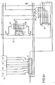
- the data inputs of circuit 19.1 are the six-wire input A used to receive the data of the pixels a -1 , b -1 , c -1 , a ' -1 , b' -1 , c ' -1 , when wire E is activated, or the pixel data a +1 . b +1 ' c +1' a ' +1 ' b ' +1' c ' +1' when wire D is activated; four-wire input B for receiving data from pixels b, c, a ', b'; and the input C making it possible to receive the data of the pixels b * +1 , a '* +1 .
- an NI gate 33 has its direct inputs connected to inputs b and b 'and its inverting inputs to inputs c and a'. Gate 33 makes it possible to detect the configuration 0110, mentioned above, in line i.
- An NI 34 door has its four direct inputs connected to wires b 1 , c 1 , a ' 1 and b' 1 .
- Gate 34 is used to detect case 1) or case 4), mentioned above.
- An NI 35 door has its two inputs connected to wires b 1 and b ' 1 , and its inverting inputs to wires c and a' 1 .
- Gate 35 is used to detect case 2) or case 5), mentioned above.
- the outputs of doors 34 and 35 are respectively connected to the two inputs of an OR gate 36, the output of which is connected to an input of an AND gate 64.
- the output of gate 34 is still connected to the input D a flip-flop 37 which has a reset input R connected to the output of an OR gate 38, one input of which is connected to the control input 39 and the other input to the control input 40, an input S of setting to one connected to the control input 41, an output Q connected to the output wire D and an output Q connected to the output wire E.
- the circuit 19.1 further comprises two calculation circuits 42 and 43 respectively carrying out the two logic calculations mentioned above.
- an AND gate 44 has its two direct inputs connected to wires c 'and c 1 ; an AND gate 45 has three direct inputs connected to wires a l , b 1 , c and an inverting input connected to wire c ' 1 ; an AND gate 46 has a direct input connected to wire c 1 and an inverting input connected to wire b; a door 47 has a direct input connected to the wire b and an inverting input connected to the wire c 1 ; an AND gate 48 has a direct input connected to wire a ' 1 and three inverting inputs connected to wires b 1 , c and a. Note that above we did not specify the sign of the index 1, because it is negative or positive according to the state of scale 37.
- the outputs of AND gates 44 and 47 are connected to the two inputs of an OR gate 49.
- the outputs of AND gates 45, 46 and 47 are connected to the three inputs of an OR gate 50.
- the output of OR gate 49 is connected to the direct input of an AND gate 51 whose inverting inputs are connected to wires a 'and b' 1 .
- the output of gate 0U 50 is connected to a direct input of an AND gate 52, the other two direct inputs of which are connected to inputs a ' 1 and b' 1 .
- the outputs of AND gates 48, 51 and 52 are connected to three inputs of an OR gate 53 of which the 4 th input is connected to the output of the AND gate 67.
- an AND gate 54 has its two direct inputs connected to wires a and a '; an AND gate 55 has three direct inputs connected to the wires a ' 1 , b' 1 , c ' 1 and an inverting input connected to the wire a l ; an AND gate 56 has a direct input connected to wire a ' 1 and its inverting input connected to wire b'; an AND gate 57 has its direct input connected to wire b ' 1 and its inverting input connected to wire a'; and an AND gate 58 has a direct input connected to wire c and three inverting inputs connected to wires a ' 1 , b' 1 and c '.
- the outputs of AND gates 54 and 56 are connected to the two inputs of an OR gate 59.
- the outputs of AND gates 55, 56 and 57 are connected to the three inputs of an OR gate 60.
- the output of OR gate 59 is connected to the direct input of an ET 61 gate whose inverting inputs are connected to wires b and c 1 .
- the output of the OR gate 60 is connected to a direct input of an AND gate 62, the other two direct inputs of which are connected to the wires b and c 1 .
- the outputs of AND gates 58, 60 and 62 are connected to three inputs of an OR gate 63, of which the 4 th input is connected to the output of the AND gate 67.
- OR gate 36 The output of the OR gate 36 is connected to an input of an AND gate 64, the other input of which is connected to the output Q of the flip-flop 37 and the output of which is connected to the first input of two OR gates 65 and 66
- the OR gates each have an activation input which is connected to the output of gate NI 33.
- the output of the gate NI 35 is still connected to an input of an AND gate 67 whose other input is connected to the output Q of the flip-flop 37 and the output of which is connected to the first input of two AND gates 68 and 69.
- the second inputs of gates 68 are respectively connected to the wires a '* +1 and b * +1 of the input C and their outputs are respectively connected to the first inputs of OR doors 65 and 66.
- the second inputs of doors 65 and 66 are respectively connected to the outputs of doors 53 and 63 and their third inputs to the outputs of doors 68 and 69.
- circuit 19.1 which is used to define the transformed pixels b ⁇ and â 'of line i.
- the circuit 19.1 operates whatever the state of the output of 33 which only serves to validate the calculations.
- the time base or logic control 12 comprises a four-stage counter 121 receiving at C the bit clock signal which it also delivers at H. Furthermore its outputs QA, QB, QC and QD are respectively connected to the two first inputs inverters, to the third non-inverting input and to the fourth inverting input of an NI 122. gate The output of gate 122 and the output H of 121 are connected to the inputs of an AND gate 123 whose output is connected to the inputs clock registers 8, 9 and 10. In addition, the outputs QA, QB, QC and QD are respectively connected to the first non-inverting input and to the other three inverting inputs of an NI 124 door. The door output 124 and the output H of 121 are connected to the inputs of an AND gate 125 whose output is connected to the clock inputs of the registers 14, 15 and 16.
- the QA and H outputs of 121 are still connected to the inputs an AND gate 126 whose output is connected to the clock inputs of registers 14 to 16.
- the circuit 12 includes another counter 127 whose input C receives the bit clock signal and whose output H 'delivers clock signals.
- the counter 127 has its QA, QB, QC and QD outputs respectively connected to the first inverting input and to the other three non-inverting inputs of an NI 128 gate, on the one hand, and to the first non-inverting input, to the second. inverting input and the other two non-inverting inputs of an NI 129 door.
- gate 128 provides the signal at the input of gates 30 and 31 of circuits 13.1 to 13.4.
- the outputs of gates 128 and 129 provide signals 40 and 41 in circuits 19.1 to 19.2.
- Fig. 9 is the diagram of an 8x10 to 12x10 conversion circuit. It includes an eight-stage shift register 130 whose data input receives the bits of the line pixels of an 8 ⁇ 10 matrix. Its outputs "1" and “2" are respectively connected to the inputs of an OR gate 131. Furthermore, the circuit comprises a twelve-stage shift register 132 which delivers the bits of the line pixels of a 12 ⁇ 10 matrix. The output "1" of 130 is connected to the parallel input "1" of 132, the output of the gate 131 is connected to the parallel input "2" of 132 and the output "2" of 130 is connected to the 'parallel input "3" of register 132. We then find the same structure three times for successively outputs "3" to "8” of 130 and inputs "4" to "12” of 132.
Landscapes
- Engineering & Computer Science (AREA)
- Physics & Mathematics (AREA)
- Computer Hardware Design (AREA)
- General Physics & Mathematics (AREA)
- Theoretical Computer Science (AREA)
- Image Processing (AREA)
- Compression, Expansion, Code Conversion, And Decoders (AREA)
- Controls And Circuits For Display Device (AREA)
- Processing Of Color Television Signals (AREA)
Applications Claiming Priority (2)
| Application Number | Priority Date | Filing Date | Title |
|---|---|---|---|
| FR8222225 | 1982-12-29 | ||
| FR8222225A FR2538979B1 (fr) | 1982-12-29 | 1982-12-29 | Systeme de transcodage de matrices pour videographie a alphabet dynamiquement redefinissable |
Publications (2)
| Publication Number | Publication Date |
|---|---|
| EP0115737A1 true EP0115737A1 (de) | 1984-08-15 |
| EP0115737B1 EP0115737B1 (de) | 1988-04-06 |
Family
ID=9280777
Family Applications (1)
| Application Number | Title | Priority Date | Filing Date |
|---|---|---|---|
| EP83460006A Expired EP0115737B1 (de) | 1982-12-29 | 1983-12-22 | Matrix-Umsetzungssystem für ein Videosystem mit einem dynamisch definierbaren Zeichensatz |
Country Status (10)
| Country | Link |
|---|---|
| US (1) | US4709232A (de) |
| EP (1) | EP0115737B1 (de) |
| JP (1) | JPS6035781A (de) |
| BR (1) | BR8307310A (de) |
| CA (1) | CA1216676A (de) |
| DE (1) | DE3376237D1 (de) |
| ES (1) | ES528499A0 (de) |
| FR (1) | FR2538979B1 (de) |
| PT (1) | PT77908B (de) |
| SU (1) | SU1479015A3 (de) |
Cited By (1)
| Publication number | Priority date | Publication date | Assignee | Title |
|---|---|---|---|---|
| FR2658681A1 (fr) * | 1990-02-21 | 1991-08-23 | Alcatel Business Systems | Procede d'adaptation d'affichage videotex pour terminal telematique. |
Families Citing this family (5)
| Publication number | Priority date | Publication date | Assignee | Title |
|---|---|---|---|---|
| JPS63205257A (ja) * | 1987-02-23 | 1988-08-24 | Oki Electric Ind Co Ltd | 印刷制御装置 |
| NL8800052A (nl) * | 1988-01-11 | 1989-08-01 | Philips Nv | Televisie-ontvanger met teletext decoder. |
| US5237316A (en) * | 1990-02-02 | 1993-08-17 | Washington University | Video display with high speed reconstruction and display of compressed images at increased pixel intensity range and retrofit kit for same |
| TW247952B (de) * | 1992-07-09 | 1995-05-21 | Seikosha Kk | |
| JP3058028B2 (ja) * | 1994-10-31 | 2000-07-04 | 三菱電機株式会社 | 画像符号化データ再符号化装置 |
Citations (1)
| Publication number | Priority date | Publication date | Assignee | Title |
|---|---|---|---|---|
| FR2419623A1 (fr) * | 1978-03-10 | 1979-10-05 | Telediffusion Fse | Systeme de transmission numerique et d'affichage de textes et de graphismes sur un ecran de television |
Family Cites Families (9)
| Publication number | Priority date | Publication date | Assignee | Title |
|---|---|---|---|---|
| US3976982A (en) * | 1975-05-12 | 1976-08-24 | International Business Machines Corporation | Apparatus for image manipulation |
| JPS526419A (en) * | 1975-07-07 | 1977-01-18 | Fuji Xerox Co Ltd | Dot matrix convertor |
| GB1581546A (en) * | 1976-07-08 | 1980-12-17 | Xenotron Ltd | Compression and expansion of scanned images |
| US4242678A (en) * | 1978-07-17 | 1980-12-30 | Dennison Manufacturing Company | Variable size character generation using neighborhood-derived shapes |
| US4479119A (en) * | 1980-07-16 | 1984-10-23 | Ricoh Company, Ltd. | CRT Display device |
| JPS5729084A (en) * | 1980-07-29 | 1982-02-16 | Ricoh Kk | Method of variably magnifying digital image |
| DE3036711C2 (de) * | 1980-09-29 | 1985-08-01 | Siemens AG, 1000 Berlin und 8000 München | Verfahren zum Verkleinern von grafischen Mustern |
| US4412252A (en) * | 1981-06-01 | 1983-10-25 | Ncr Corporation | Image reduction system |
| US4532602A (en) * | 1982-03-08 | 1985-07-30 | The Mead Corporation | Device for electrical variable magnification of document image |
-
1982
- 1982-12-29 FR FR8222225A patent/FR2538979B1/fr not_active Expired
-
1983
- 1983-12-16 US US06/562,431 patent/US4709232A/en not_active Expired - Fee Related
- 1983-12-22 DE DE8383460006T patent/DE3376237D1/de not_active Expired
- 1983-12-22 EP EP83460006A patent/EP0115737B1/de not_active Expired
- 1983-12-26 SU SU833683855A patent/SU1479015A3/ru active
- 1983-12-28 JP JP58245636A patent/JPS6035781A/ja active Pending
- 1983-12-28 ES ES528499A patent/ES528499A0/es active Granted
- 1983-12-29 BR BR8307310A patent/BR8307310A/pt not_active IP Right Cessation
- 1983-12-29 CA CA000444459A patent/CA1216676A/en not_active Expired
- 1983-12-29 PT PT77908A patent/PT77908B/pt not_active IP Right Cessation
Patent Citations (1)
| Publication number | Priority date | Publication date | Assignee | Title |
|---|---|---|---|---|
| FR2419623A1 (fr) * | 1978-03-10 | 1979-10-05 | Telediffusion Fse | Systeme de transmission numerique et d'affichage de textes et de graphismes sur un ecran de television |
Cited By (2)
| Publication number | Priority date | Publication date | Assignee | Title |
|---|---|---|---|---|
| FR2658681A1 (fr) * | 1990-02-21 | 1991-08-23 | Alcatel Business Systems | Procede d'adaptation d'affichage videotex pour terminal telematique. |
| EP0445562A1 (de) * | 1990-02-21 | 1991-09-11 | Alcatel Business Systems | Verfahren zur Anpassung einer Videotexanzeige an ein telematisches Terminal |
Also Published As
| Publication number | Publication date |
|---|---|
| PT77908B (fr) | 1986-03-27 |
| PT77908A (fr) | 1984-01-01 |
| ES8500537A1 (es) | 1984-10-01 |
| JPS6035781A (ja) | 1985-02-23 |
| FR2538979A1 (fr) | 1984-07-06 |
| SU1479015A3 (ru) | 1989-05-07 |
| DE3376237D1 (en) | 1988-05-11 |
| FR2538979B1 (fr) | 1985-07-05 |
| BR8307310A (pt) | 1984-08-14 |
| CA1216676A (en) | 1987-01-13 |
| US4709232A (en) | 1987-11-24 |
| ES528499A0 (es) | 1984-10-01 |
| EP0115737B1 (de) | 1988-04-06 |
Similar Documents
| Publication | Publication Date | Title |
|---|---|---|
| EP0142439B1 (de) | Verfahren zur Kompression einer Folge digitaler Informationen und Vorrichtung dafür | |
| JP3038219B2 (ja) | ディジタル化されたアナログ信号を表すデータ語の送受信デバイス | |
| EP0206847B1 (de) | Rechnungseinrichtungen von Cosinustransformationen, solche Rechnungseinrichtungen enthaltende Kodierungs- und Dekodierungseinrichtung von Bildern | |
| US5568597A (en) | Adapting image data resolution to match resolution of an output device | |
| FR2585915A1 (fr) | Appareil de correction de depassements d'un signal numerique | |
| EP0115737B1 (de) | Matrix-Umsetzungssystem für ein Videosystem mit einem dynamisch definierbaren Zeichensatz | |
| US4797806A (en) | High speed serial pixel neighborhood processor and method | |
| EP0041001A1 (de) | Digitale Bit-für-Bit Zeitmultiplex-Fernmeldekoppelfelder | |
| US5485412A (en) | Method and apparatus for successive horizontal and vertical data filtering | |
| FR2543770A1 (fr) | Procede et systeme de condensation de donnees d'images binaires | |
| US5309438A (en) | ATM cell delay circuit for ISDN system | |
| CA2001068C (fr) | Procede de transmission de donnees sur un bus interne d'une station de travail, dispositif a bus interne, permettant la mise en oeuvre du procede, et circuit d'adaptation pour ce bus interne | |
| US5046117A (en) | Image data scaling system | |
| EP0317463B1 (de) | Schaltungsanordnung zur Herstellung von Konferenzverbindungen mehrerer Teilnehmer in Fernmeldesystemen | |
| US3720875A (en) | Differential encoding with lookahead feature | |
| EP0476592A2 (de) | Adressengenerator für den Datenspeicher eines Prozessors | |
| US5544091A (en) | Circuit scale reduction for bit-serial digital signal processing | |
| US5463714A (en) | Sound data interpolating circuit | |
| FR2534765A1 (fr) | Commutateur temporel de donnees et de communications de conference | |
| EP0205523B1 (de) | Einrichtung zur simultanen aktivierung von befehlsfolgen und ihre verwendung in speichern | |
| KR100276768B1 (ko) | 화상데이타의 부호화를 위한 변화화소 검출기 | |
| EP0365878B1 (de) | Bildverarbeitungsverfahren | |
| JP2516611B2 (ja) | 並列デ−タ処理装置 | |
| JP3850040B2 (ja) | 文脈上の相関関係を使用するパターン認識方法及び装置 | |
| JP2577797B2 (ja) | 画素密度変換回路 |
Legal Events
| Date | Code | Title | Description |
|---|---|---|---|
| PUAI | Public reference made under article 153(3) epc to a published international application that has entered the european phase |
Free format text: ORIGINAL CODE: 0009012 |
|
| AK | Designated contracting states |
Designated state(s): CH DE GB IT LI NL SE |
|
| 17P | Request for examination filed |
Effective date: 19841218 |
|
| 17Q | First examination report despatched |
Effective date: 19870402 |
|
| ITF | It: translation for a ep patent filed | ||
| GRAA | (expected) grant |
Free format text: ORIGINAL CODE: 0009210 |
|
| AK | Designated contracting states |
Kind code of ref document: B1 Designated state(s): CH DE GB IT LI NL SE |
|
| GBT | Gb: translation of ep patent filed (gb section 77(6)(a)/1977) | ||
| REF | Corresponds to: |
Ref document number: 3376237 Country of ref document: DE Date of ref document: 19880511 |
|
| PLBE | No opposition filed within time limit |
Free format text: ORIGINAL CODE: 0009261 |
|
| STAA | Information on the status of an ep patent application or granted ep patent |
Free format text: STATUS: NO OPPOSITION FILED WITHIN TIME LIMIT |
|
| 26N | No opposition filed | ||
| PGFP | Annual fee paid to national office [announced via postgrant information from national office to epo] |
Ref country code: GB Payment date: 19911031 Year of fee payment: 9 |
|
| PGFP | Annual fee paid to national office [announced via postgrant information from national office to epo] |
Ref country code: SE Payment date: 19911105 Year of fee payment: 9 |
|
| ITTA | It: last paid annual fee | ||
| PG25 | Lapsed in a contracting state [announced via postgrant information from national office to epo] |
Ref country code: GB Effective date: 19921222 |
|
| PG25 | Lapsed in a contracting state [announced via postgrant information from national office to epo] |
Ref country code: SE Effective date: 19921223 |
|
| GBPC | Gb: european patent ceased through non-payment of renewal fee |
Effective date: 19921222 |
|
| EUG | Se: european patent has lapsed |
Ref document number: 83460006.6 Effective date: 19930709 |
|
| PGFP | Annual fee paid to national office [announced via postgrant information from national office to epo] |
Ref country code: DE Payment date: 19971120 Year of fee payment: 15 |
|
| PGFP | Annual fee paid to national office [announced via postgrant information from national office to epo] |
Ref country code: CH Payment date: 19971125 Year of fee payment: 15 |
|
| PGFP | Annual fee paid to national office [announced via postgrant information from national office to epo] |
Ref country code: NL Payment date: 19981123 Year of fee payment: 16 |
|
| PG25 | Lapsed in a contracting state [announced via postgrant information from national office to epo] |
Ref country code: LI Free format text: LAPSE BECAUSE OF NON-PAYMENT OF DUE FEES Effective date: 19981231 Ref country code: CH Free format text: LAPSE BECAUSE OF NON-PAYMENT OF DUE FEES Effective date: 19981231 |
|
| PG25 | Lapsed in a contracting state [announced via postgrant information from national office to epo] |
Ref country code: NL Free format text: LAPSE BECAUSE OF NON-PAYMENT OF DUE FEES Effective date: 19990701 |
|
| REG | Reference to a national code |
Ref country code: CH Ref legal event code: PL |
|
| NLV4 | Nl: lapsed or anulled due to non-payment of the annual fee |
Effective date: 19990701 |
|
| PG25 | Lapsed in a contracting state [announced via postgrant information from national office to epo] |
Ref country code: DE Free format text: LAPSE BECAUSE OF NON-PAYMENT OF DUE FEES Effective date: 19991001 |