EP0067573B1 - Antennegruppen - Google Patents
Antennegruppen Download PDFInfo
- Publication number
- EP0067573B1 EP0067573B1 EP82302702A EP82302702A EP0067573B1 EP 0067573 B1 EP0067573 B1 EP 0067573B1 EP 82302702 A EP82302702 A EP 82302702A EP 82302702 A EP82302702 A EP 82302702A EP 0067573 B1 EP0067573 B1 EP 0067573B1
- Authority
- EP
- European Patent Office
- Prior art keywords
- guide
- array
- feeder
- radiators
- sheet
- Prior art date
- Legal status (The legal status is an assumption and is not a legal conclusion. Google has not performed a legal analysis and makes no representation as to the accuracy of the status listed.)
- Expired
Links
- 238000003491 array Methods 0.000 title description 10
- 230000008878 coupling Effects 0.000 claims description 8
- 238000010168 coupling process Methods 0.000 claims description 8
- 238000005859 coupling reaction Methods 0.000 claims description 8
- 239000000463 material Substances 0.000 claims description 5
- 239000003989 dielectric material Substances 0.000 claims description 3
- 230000000694 effects Effects 0.000 claims description 2
- 230000005855 radiation Effects 0.000 description 14
- 239000000523 sample Substances 0.000 description 3
- 230000005684 electric field Effects 0.000 description 2
- 238000013461 design Methods 0.000 description 1
- 238000005259 measurement Methods 0.000 description 1
- 230000007246 mechanism Effects 0.000 description 1
- 239000002184 metal Substances 0.000 description 1
- 238000000034 method Methods 0.000 description 1
- 230000004048 modification Effects 0.000 description 1
- 238000012986 modification Methods 0.000 description 1
- 230000035699 permeability Effects 0.000 description 1
- 238000012216 screening Methods 0.000 description 1
- 239000000758 substrate Substances 0.000 description 1
Images
Classifications
-
- H—ELECTRICITY
- H01—ELECTRIC ELEMENTS
- H01Q—ANTENNAS, i.e. RADIO AERIALS
- H01Q13/00—Waveguide horns or mouths; Slot antennas; Leaky-waveguide antennas; Equivalent structures causing radiation along the transmission path of a guided wave
- H01Q13/20—Non-resonant leaky-waveguide or transmission-line antennas; Equivalent structures causing radiation along the transmission path of a guided wave
- H01Q13/206—Microstrip transmission line antennas
-
- H—ELECTRICITY
- H01—ELECTRIC ELEMENTS
- H01Q—ANTENNAS, i.e. RADIO AERIALS
- H01Q21/00—Antenna arrays or systems
- H01Q21/0006—Particular feeding systems
- H01Q21/0037—Particular feeding systems linear waveguide fed arrays
- H01Q21/0068—Dielectric waveguide fed arrays
Definitions
- This invention relates to antenna arrays.
- Microstrip arrays are known, e.g. as described in British Patent Specification 1,529,361, which comprise a plurality of strips of metallising formed on the surface of an insulating substrate backed by a metallic ground-plane, the strips extending at regular intervals from a feeder strip of similar metallising.
- arrays are suitable at microwave frequencies, e.g. in the range 3-30 GHz (free-space wavelength 1-10cm), at millimetre (free-space) wavelengths such microstrip feeders become very lossy.
- British Patent Specification 1,572,273 shows somewhat similar structures in which the inner ends of the strips are spaced from the feeder strip.
- dielectric image waveguides are less lossy than microstrip lines at millimetre wavelengths.
- Birand et al describe an array comprising a dielectric image waveguide acting as a feeder, the guider being of the insular type and having a sheet of dielectric material on its upper surface. On the upper surface of this sheet is printed by metallising a plurality of dipoles spaced regularly along the guide.
- this "twin-deck" structure is relatively complex and therefore expensive, and does not readily lend itself to use in conformal arrays, i.e. arrays which conform with the surface (which may be curved) of an aircraft or missile to which they are applied.
- the latter is one of the known advantages of printed microstrip antennas.
- the present antennas give better control of the radiation pattern than do known millimetre antennas which use dielectric image waveguides provided with notches to act as radiating elements.
- an antenna array comprising a longitudinal extending image feeder-guide of the insular type comprising a dielectric sheet backed by a conducting ground-plane and having the guide in contact with the other surface of the sheet, the relative permittivity of the guide material being greater than that of the sheet material, and having a plurality of conducting-sheet radiators on the surface of a sheet of dielectric material which is in contact with said guide, said radiators being coupled to said guide, being spaced at intervals along this length, and being dimensioned to be resonant at the operating frequency of the array, is characterised by the said radiators being on the same surface of said first-mentioned sheet as is contacted by the feeder-guide itself, the inner edges of the radiators being located relative to the sides of the feeder-guide so as to effect electromagnetic coupling with the guide.
- the inner edges of the radiators may be spaced outward from the side of the feeder-guide, may contact the side of the feeder-guide, or may underlie the side of the feeder-guide.
- the radiators may be strips approximately a half-wavelength long extending outwards from the sides of the feeder-guide.
- the strips may be spaced along either or both sides of the feeder-guide and, for broadside radiation, are suitably located at wavelength intervals (i.e. the wavelength in the guide) therealong at one or each side. As previously stated the strips are suitably approximately a half-wavelength long (i.e. a half-wavelength in the strip) for matching purposes.
- the strips may extend at right angles to the feeder-guide or may be inclined at an angle thereto, e.g. strips angled at 45° with those on one side spaced a quarter-wavelength from those on the other will give circular polarisation.
- the feeder-guide and the wavelauncher thereinto may be adapted to propagate in the guide a mode which is higher than the fundamental mode, suitably the mode rather than the Er, mode, in order to promote good coupling between the guide wmd the strips and thereby improve the efficiency and resulting radiation pattern of the array (the overall pattern being affected not only by radiation from the strips themselves, but by any unwanted radiation from the launcher and termination).
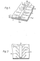
- Fig. 1 a conventional insular image waveguide system comprising a dielectric sheet 1 having a conducting ground-plane 2 on its under surface and a rectangular cross-section dielectric waveguide 3 on its upper surface.
- the relative permittivity of guide 3, ⁇ r is greater than that of sheet 1, Er g, in a known manner.
- Spaced along each side of guide 3 is a plurality of strips 4 of metallising applied, e.g. by conventional printing, to the upper surface of sheet 1.
- the strips on one side are spaced halfway between those on the other side, and the distance between adjacent strips on each side is 2D.
- intended to produce broadside radiation i.e.
- each strip is spaced from the guide 3 by a distance d and the strip width is w.
- the guide width and height are respectively 2a and b, and the thickness of sheet 1 is h.
- the input or output connection to one end of guide 3 is made in a conventional manner.
- the other end may be terminated with the characteristic impedance of the guide for operation in a travelling-wave mode, or left open-circuit for operation in a resonant mode.
- the radiation is likewise, as therein, primarily from the outer ends of the strips 4 which can be regarded as acting as oscillating magnetic dipoles, as indicated by the arrow 5. With the described spacing, all the dipoles oscillate in phase so that the main beam is normal to the plane of the array, but the spacing can be altered to vary its direction in a known manner.
- microstrip radiators 4 with a dielectric image waveguide feeder allows the values of h and ⁇ rg to be chosen so as to achieve efficient radiation from the strips 4, while avoiding the losses at millimetre wavelengths which use of a microstrip feeder, as in the aforementioned British Patent, would involve.
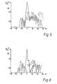
- the percentage is plotted against a/ ⁇ o .
- the E y mn mode type designates a hybrid mode with both E and H fields along the propagation direction but with a predominantly vertical (y) E field.
- Suffixes m and n indicate the number of modes in the transverse x and y directions. It can be seen that the degree of coupling is considerably higher for the E y 21 mode than for the fundamental mode Er 1 and for this reason the embodiments to be described were designed on the basis of the higher order mode. The accuracy of these estimations is limited by the approximations taken; the effective dielectric-constant method described by McLevige et al (see above reference) is used, approximating both ⁇ 1 and the field forms within the guide 3. Tighter coupling may be obtained by causing the strips 4 to extend inwards under the guide 3, i.e. making d negative, in which case some adjustment of the strip length may be necessary.
- Embodiments of the array of Fig. 1 have been constructed for use at 14 and 70GHz, the latter being scaled-down versions of the former, for operation in both the resonant and travelling-wave modes.
- the guide 3 was operated in the E y 21 mode.
- the angle 8 is the angle made with the normal to the plane of the array in the plane of the array axis (see Fig. 1), and E. is the electric field strength in the direction 8.
- the launcher comprised a 1mm wide metal strip extending between the guide 3 and the sheet 1, which was tuned to a length of 15mm for optimum VSWR at the coaxial feed; the guide 3 was tapered in height over the metal-strip probe in a known manner. The residual unradiated power at the termination of guide 3 was absorbed into a lossy painted load. Calculations based on Fig.
- Fig. 4 shows the radiation pattern of the 14 GHz array in the resonant mode, using the same probe/coaxial launcher as for Fig. 3.
- the launcher radiation was screened by lossy material, and cross-polarisation was further reduced to less than -15dB by screening the terminations. Improvements in the side-lobe levels may be obtainable by tapering the widths of the strips 4 along the lengths of the arrays.
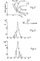
- Fig. 7 shows further embodiment, but with the strips 24 angled at 45° to the axis of the guide 23 so that the notional dipoles 25 at their outer ends are similarly angled. Also, the strips on one side, instead being midway, i.e. A,/2, between those on the other side, are located at a spacing A l /4 relative thereto, as shown. In consequence, a circularly polarised radiation pattern is obtained.
- Other relevant variations in strip width and spacing can be adopted in a manner similar to that described in the aforesaid British Patent 1,529,361, in order to obtain corresponding results.
- the described embodiments use an image guide feeder of rectangular cross-section, but this is not essential.
Landscapes
- Variable-Direction Aerials And Aerial Arrays (AREA)
- Waveguide Aerials (AREA)
Claims (9)
Applications Claiming Priority (4)
| Application Number | Priority Date | Filing Date | Title |
|---|---|---|---|
| GB8118509 | 1981-06-16 | ||
| GB8118509 | 1981-06-16 | ||
| GB8121408 | 1981-07-10 | ||
| GB8121408 | 1981-07-10 |
Publications (2)
| Publication Number | Publication Date |
|---|---|
| EP0067573A1 EP0067573A1 (de) | 1982-12-22 |
| EP0067573B1 true EP0067573B1 (de) | 1986-03-19 |
Family
ID=26279815
Family Applications (1)
| Application Number | Title | Priority Date | Filing Date |
|---|---|---|---|
| EP82302702A Expired EP0067573B1 (de) | 1981-06-16 | 1982-05-26 | Antennegruppen |
Country Status (3)
| Country | Link |
|---|---|
| US (1) | US4507664A (de) |
| EP (1) | EP0067573B1 (de) |
| DE (1) | DE3269949D1 (de) |
Families Citing this family (13)
| Publication number | Priority date | Publication date | Assignee | Title |
|---|---|---|---|---|
| US4677404A (en) * | 1984-12-19 | 1987-06-30 | Martin Marietta Corporation | Compound dielectric multi-conductor transmission line |
| JPH0682974B2 (ja) * | 1985-04-17 | 1994-10-19 | 日本電装株式会社 | 携帯型受信アンテナ装置 |
| JPH027611A (ja) * | 1988-06-24 | 1990-01-11 | Murata Mfg Co Ltd | 静磁波装置 |
| US5107231A (en) * | 1989-05-25 | 1992-04-21 | Epsilon Lambda Electronics Corp. | Dielectric waveguide to TEM transmission line signal launcher |
| US5061915A (en) * | 1990-05-22 | 1991-10-29 | Murphy Del A | Anti-theft device for motorized vehicles |
| WO2000033414A2 (en) | 1998-11-03 | 2000-06-08 | Arizona Board Or Regents | Frequency selective microwave devices using narrowband metal materials |
| RU2190907C2 (ru) * | 2000-09-26 | 2002-10-10 | Омский государственный технический университет | Вибраторная решетка |
| US6801164B2 (en) | 2001-08-27 | 2004-10-05 | Motorola, Inc. | Broad band and multi-band antennas |
| US8009107B2 (en) * | 2006-12-04 | 2011-08-30 | Agc Automotive Americas R&D, Inc. | Wideband dielectric antenna |
| US10312596B2 (en) * | 2013-01-17 | 2019-06-04 | Hrl Laboratories, Llc | Dual-polarization, circularly-polarized, surface-wave-waveguide, artificial-impedance-surface antenna |
| US20150222022A1 (en) * | 2014-01-31 | 2015-08-06 | Nathan Kundtz | Interleaved orthogonal linear arrays enabling dual simultaneous circular polarization |
| US10983194B1 (en) | 2014-06-12 | 2021-04-20 | Hrl Laboratories, Llc | Metasurfaces for improving co-site isolation for electronic warfare applications |
| CN108448239B (zh) * | 2018-02-28 | 2019-11-15 | 维沃移动通信有限公司 | 一种毫米波天线阵列及移动终端 |
Family Cites Families (18)
| Publication number | Priority date | Publication date | Assignee | Title |
|---|---|---|---|---|
| US2761137A (en) * | 1946-01-05 | 1956-08-28 | Lester C Van Atta | Solid dielectric waveguide with metal plating |
| US2993205A (en) * | 1955-08-19 | 1961-07-18 | Litton Ind Of Maryland Inc | Surface wave antenna array with radiators for coupling surface wave to free space wave |
| US2929065A (en) * | 1957-02-27 | 1960-03-15 | Hughes Aircraft Co | Surface wave antenna |
| US3225351A (en) * | 1962-03-09 | 1965-12-21 | Maurice G Chatelain | Vertically polarized microstrip antenna for glide path system |
| US3155975A (en) * | 1962-05-07 | 1964-11-03 | Ryan Aeronautical Co | Circular polarization antenna composed of an elongated microstrip with a plurality of space staggered radiating elements |
| US3283330A (en) * | 1962-05-28 | 1966-11-01 | Ryan Aeronautical Co | Omnipolarization microstrip antenna |
| US3568208A (en) * | 1968-10-22 | 1971-03-02 | Raytheon Co | Varying propagation constant waveguide |
| US3771077A (en) * | 1970-09-24 | 1973-11-06 | F Tischer | Waveguide and circuit using the waveguide to interconnect the parts |
| GB1529361A (en) * | 1975-02-17 | 1978-10-18 | Secr Defence | Stripline antenna arrays |
| US4054874A (en) * | 1975-06-11 | 1977-10-18 | Hughes Aircraft Company | Microstrip-dipole antenna elements and arrays thereof |
| US4091343A (en) * | 1975-06-30 | 1978-05-23 | Epsilon Lambda Electronics Corp. | Insular waveguide directional coupler |
| US4028643A (en) * | 1976-05-12 | 1977-06-07 | University Of Illinois Foundation | Waveguide having strip dielectric structure |
| GB1572273A (en) * | 1977-05-31 | 1980-07-30 | Emi Ltd | Aerial arrangements |
| GB1566772A (en) * | 1977-09-15 | 1980-05-08 | Standard Telephones Cables Ltd | Microstrip antenna radiators |
| JPS5597703A (en) * | 1978-01-05 | 1980-07-25 | Naohisa Goto | Circularly polarized wave antenna |
| GB2064877B (en) * | 1979-11-22 | 1983-07-27 | Secr Defence | Microstrip antenna |
| US4378558A (en) * | 1980-08-01 | 1983-03-29 | The Boeing Company | Endfire antenna arrays excited by proximity coupling to single wire transmission line |
| GB2097196B (en) * | 1981-04-22 | 1984-09-05 | Era Patents Ltd | Millimeter wave arrays |
-
1982
- 1982-05-26 DE DE8282302702T patent/DE3269949D1/de not_active Expired
- 1982-05-26 EP EP82302702A patent/EP0067573B1/de not_active Expired
- 1982-06-16 US US06/389,069 patent/US4507664A/en not_active Expired - Fee Related
Non-Patent Citations (1)
| Title |
|---|
| ELECTRONICS LETTERS, vol. 17, no. 3, 5th February 1981, pages 146-147, London (GB); M.T. BIRAND et al.: "Experimental 30 GHz printed array with low loss insular guide feeder" * |
Also Published As
| Publication number | Publication date |
|---|---|
| EP0067573A1 (de) | 1982-12-22 |
| DE3269949D1 (en) | 1986-04-24 |
| US4507664A (en) | 1985-03-26 |
Similar Documents
| Publication | Publication Date | Title |
|---|---|---|
| EP0456680B1 (de) | Gruppenantennen | |
| CA1261060A (en) | Planar antenna with patch radiators | |
| US5349363A (en) | Antenna array configurations employing continuous transverse stub elements | |
| US5483248A (en) | Continuous transverse stub element devices for flat plate antenna arrays | |
| US4238798A (en) | Stripline antennae | |
| US5461392A (en) | Transverse probe antenna element embedded in a flared notch array | |
| US4063246A (en) | Coplanar stripline antenna | |
| EP2293380B1 (de) | Übergang zwischen Triplate-Leitungen und planare Gruppenantenne | |
| US4173019A (en) | Microstrip antenna array | |
| KR920002896B1 (ko) | 슬롯트형, 도파관 안테나 | |
| US2914766A (en) | Three conductor planar antenna | |
| CN113823891B (zh) | 天线模组、毫米波雷达以及车辆 | |
| EP0067573B1 (de) | Antennegruppen | |
| EP0922312B1 (de) | Planare antennenstrahlungsstruktur mit quasi-abtastung, frequenzunabhängiger speisepunkt- impedanz | |
| US8736514B2 (en) | Antenna | |
| EP0257881A2 (de) | Geschlitzte Hohlleiterantenne und ihre Anordnung in der Gruppe | |
| CA2017766A1 (en) | Annular slot antenna | |
| US4618865A (en) | Dielectric trough waveguide antenna | |
| EP0228131A2 (de) | Streifenleiterantennengruppe | |
| US3523297A (en) | Dual frequency antenna | |
| US5170174A (en) | Patch-excited non-inclined radiating slot waveguide | |
| CN102683858B (zh) | 天线 | |
| US5467098A (en) | Transmission line notch antenna | |
| WO1996010277A9 (en) | Planar high gain microwave antenna | |
| Sakakibara et al. | A slotted waveguide array using reflection-cancelling slot pairs |
Legal Events
| Date | Code | Title | Description |
|---|---|---|---|
| PUAI | Public reference made under article 153(3) epc to a published international application that has entered the european phase |
Free format text: ORIGINAL CODE: 0009012 |
|
| AK | Designated contracting states |
Designated state(s): DE FR GB IT NL |
|
| 17P | Request for examination filed |
Effective date: 19830511 |
|
| GRAA | (expected) grant |
Free format text: ORIGINAL CODE: 0009210 |
|
| ITF | It: translation for a ep patent filed | ||
| AK | Designated contracting states |
Kind code of ref document: B1 Designated state(s): DE FR GB IT NL |
|
| REF | Corresponds to: |
Ref document number: 3269949 Country of ref document: DE Date of ref document: 19860424 |
|
| ET | Fr: translation filed | ||
| PLBE | No opposition filed within time limit |
Free format text: ORIGINAL CODE: 0009261 |
|
| STAA | Information on the status of an ep patent application or granted ep patent |
Free format text: STATUS: NO OPPOSITION FILED WITHIN TIME LIMIT |
|
| 26N | No opposition filed | ||
| ITTA | It: last paid annual fee | ||
| PGFP | Annual fee paid to national office [announced via postgrant information from national office to epo] |
Ref country code: FR Payment date: 19940413 Year of fee payment: 13 |
|
| PGFP | Annual fee paid to national office [announced via postgrant information from national office to epo] |
Ref country code: GB Payment date: 19940419 Year of fee payment: 13 |
|
| PGFP | Annual fee paid to national office [announced via postgrant information from national office to epo] |
Ref country code: DE Payment date: 19940425 Year of fee payment: 13 |
|
| PGFP | Annual fee paid to national office [announced via postgrant information from national office to epo] |
Ref country code: NL Payment date: 19940531 Year of fee payment: 13 |
|
| PG25 | Lapsed in a contracting state [announced via postgrant information from national office to epo] |
Ref country code: GB Effective date: 19950526 |
|
| PG25 | Lapsed in a contracting state [announced via postgrant information from national office to epo] |
Ref country code: NL Effective date: 19951201 |
|
| GBPC | Gb: european patent ceased through non-payment of renewal fee |
Effective date: 19950526 |
|
| NLV4 | Nl: lapsed or anulled due to non-payment of the annual fee |
Effective date: 19951201 |
|
| PG25 | Lapsed in a contracting state [announced via postgrant information from national office to epo] |
Ref country code: DE Effective date: 19960201 |
|
| PG25 | Lapsed in a contracting state [announced via postgrant information from national office to epo] |
Ref country code: FR Effective date: 19960229 |
|
| REG | Reference to a national code |
Ref country code: FR Ref legal event code: ST |
|
| REG | Reference to a national code |
Ref country code: FR Ref legal event code: ST |