EP0067575B1 - Dispositif semiconducteur de puissance - Google Patents
Dispositif semiconducteur de puissance Download PDFInfo
- Publication number
- EP0067575B1 EP0067575B1 EP19820302716 EP82302716A EP0067575B1 EP 0067575 B1 EP0067575 B1 EP 0067575B1 EP 19820302716 EP19820302716 EP 19820302716 EP 82302716 A EP82302716 A EP 82302716A EP 0067575 B1 EP0067575 B1 EP 0067575B1
- Authority
- EP
- European Patent Office
- Prior art keywords
- case
- semiconductor element
- support plate
- electrode
- element structure
- Prior art date
- Legal status (The legal status is an assumption and is not a legal conclusion. Google has not performed a legal analysis and makes no representation as to the accuracy of the status listed.)
- Expired
Links
Images


Classifications
-
- H—ELECTRICITY
- H10—SEMICONDUCTOR DEVICES; ELECTRIC SOLID-STATE DEVICES NOT OTHERWISE PROVIDED FOR
- H10W—GENERIC PACKAGES, INTERCONNECTIONS, CONNECTORS OR OTHER CONSTRUCTIONAL DETAILS OF DEVICES COVERED BY CLASS H10
- H10W72/00—Interconnections or connectors in packages
- H10W72/30—Die-attach connectors
-
- H—ELECTRICITY
- H10—SEMICONDUCTOR DEVICES; ELECTRIC SOLID-STATE DEVICES NOT OTHERWISE PROVIDED FOR
- H10W—GENERIC PACKAGES, INTERCONNECTIONS, CONNECTORS OR OTHER CONSTRUCTIONAL DETAILS OF DEVICES COVERED BY CLASS H10
- H10W76/00—Containers; Fillings or auxiliary members therefor; Seals
- H10W76/10—Containers or parts thereof
- H10W76/12—Containers or parts thereof characterised by their shape
- H10W76/13—Containers comprising a conductive base serving as an interconnection
- H10W76/134—Containers comprising a conductive base serving as an interconnection having other interconnections parallel to the conductive base
-
- H—ELECTRICITY
- H10—SEMICONDUCTOR DEVICES; ELECTRIC SOLID-STATE DEVICES NOT OTHERWISE PROVIDED FOR
- H10W—GENERIC PACKAGES, INTERCONNECTIONS, CONNECTORS OR OTHER CONSTRUCTIONAL DETAILS OF DEVICES COVERED BY CLASS H10
- H10W78/00—Detachable holders for supporting packaged chips in operation
-
- H—ELECTRICITY
- H10—SEMICONDUCTOR DEVICES; ELECTRIC SOLID-STATE DEVICES NOT OTHERWISE PROVIDED FOR
- H10W—GENERIC PACKAGES, INTERCONNECTIONS, CONNECTORS OR OTHER CONSTRUCTIONAL DETAILS OF DEVICES COVERED BY CLASS H10
- H10W90/00—Package configurations
-
- H—ELECTRICITY
- H10—SEMICONDUCTOR DEVICES; ELECTRIC SOLID-STATE DEVICES NOT OTHERWISE PROVIDED FOR
- H10W—GENERIC PACKAGES, INTERCONNECTIONS, CONNECTORS OR OTHER CONSTRUCTIONAL DETAILS OF DEVICES COVERED BY CLASS H10
- H10W72/00—Interconnections or connectors in packages
- H10W72/071—Connecting or disconnecting
- H10W72/073—Connecting or disconnecting of die-attach connectors
-
- H—ELECTRICITY
- H10—SEMICONDUCTOR DEVICES; ELECTRIC SOLID-STATE DEVICES NOT OTHERWISE PROVIDED FOR
- H10W—GENERIC PACKAGES, INTERCONNECTIONS, CONNECTORS OR OTHER CONSTRUCTIONAL DETAILS OF DEVICES COVERED BY CLASS H10
- H10W72/00—Interconnections or connectors in packages
- H10W72/071—Connecting or disconnecting
- H10W72/073—Connecting or disconnecting of die-attach connectors
- H10W72/07331—Connecting techniques
- H10W72/07337—Connecting techniques using a polymer adhesive, e.g. an adhesive based on silicone or epoxy
Definitions
- This invention relates to power semiconductor devices, the hermetical seal of which is improved.
- Power semiconductor devices for rectifiers or the like used for fork lifts and electric cars generally have high current capacities and, therefore, require large element areas. Therefore, thermal fatigue of soldered portions of electrodes and breakage of bonding wires due to fusion are liable. Desirably, these devices are free from soldering or bonding. Meanwhile, these devices should desirably have a flat top surface for various parts which have to be mounted thereon. Further, a high permetical seal must be ensured lest water should intrude into the inner element section in such case as when washing the vehicle.
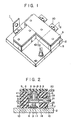
- Figs. 1 and 2 To meet these requirements, there has been proposed construction as shown in Figs. 1 and 2. The construction is free from soldering and bonding and uses a spring member which is held in a compression bonded state. It has a flat top surface, and an electrode is adapted to be taken out in a lateral direction. Further, hermetical seal of the inside is ensured by using 0-rings. More particularly, referring to Figs. 1 and 2, on an aluminum support plate 2 which also serves as a heat radiator is supported a compression bonding type semiconductor element 4 such as a diode such that its anode electrode 3 is in contact with the top of the support plate 2. On the aluminum support plate 2 is also supported a case 5 made of a resin such that it is open at both its upper and . lower ends.
- a compression bonding type semiconductor element 4 such as a diode such that its anode electrode 3 is in contact with the top of the support plate 2.
- case 5 made of a resin such that it is open at both its upper and .
- the case 5 surrounds the semiconductor element 4.
- a cover plate 6 seals the top opening of the case 5.
- the aluminum support plate 2, case 5 and cover plate 6 are secured to one another by suitable securing means such as a plurality of screws 7.
- suitable securing means such as a plurality of screws 7.
- At least either one of the confronting surfaces of the case 5 and cover plate 6, for instance the confronting surface of the case 5, is provided with a groove surrounding the open top.
- An O-ring 9 which is made of an elastic insulator is received in the groove 8 and compressed by the cover plate 6.
- the interior of the case 5 is thus hermetically sealed.
- the aluminum support plate 2 is provided with recesses 10 so that the screws 7 will not project from the support plate 2.
- An electrode body 13 is disposed over the cathode electrode 11 of the semiconductor element 4.
- a metal stud 12 such as molybdenum or tungsten having substantially the same coefficient of thermal expansion as that of the semiconductor material, for instance silicon in order to prevent cracking of the element 3 due to thermal fatigue.
- a cathode lead electrode 15 On the electrode body 13 is provided one end of a cathode lead electrode 15, which has its other end extending through a hole 14 formed in a side wall of the case 5.
- a cathode lead electrode 15 over the semiconductor element are mounted via an insulator 16 and a washer 17 a plurality of dish springs 18.
- the dish springs 18 are urged toward the semiconductor element 4. That is, the semiconductor element 4 and cathode lead electrode 15 are secured in an urged state on the aluminum support plate 2 by the dish springs 18.
- a guide 19 Extending centrally of the dish springs 18 is a guide 19 for guiding the dish springs.
- An L-shaped cathode lead electrode 20 is secured by a screw 21 to the outer side face of the cathode lead electrode 15.
- FR-A-2 341 945 discloses a power semiconductor device having a support member which serves as a heat radiator.
- a semiconductor element is supported on the support member and electrically connected thereto.
- a case surrounds the semiconductor element; a lead electrode is electrically connected to the semiconductor element and is led out to the outside of the case through an aperture in a side wall thereof.
- a spring disposed inside the case urges the lead electrode and the semiconductor element towards the support member. The spring is held in a predetermined bias position and means are provided for holding the case, the parts accommodated in the case, and the support member together.
- An object of this invention is to provide a power semiconductor device, in which an O-ring can be uniformly deformed to steadily obtain a hermetical seal irrespective of the tolerances of parts.
- a power semiconductor device comprising a support plate also serving as a heat radiator, a semiconductor element structure supported on said support plate and electrically connected thereto, a case which surrounds said semiconductor element structure, a lead electrode electrically connected to said semiconductor element structure and lead out to the outside of the case through an aperture in a side wall thereof, a spring structure disposed inside said case and urging said lead electrode and the semiconductor element structure toward said support plate, a cover for holding said spring structure in a predetermined biased state, and fastening means for holding said case, the parts accommodated therein, and said support plate together; characterised in that said case is provided on said support plate, a spacing electrode is provided between said lead electrode and said semiconductor element structure, said aperture is sized to provide a clearance between the lead electrode and the aperture and is spaced axially from said semiconductor element structure a distance sufficient to provide an uninterrupted annular portion of the inner wall of said case, and an 0-ring is clamped between the outer periphery of said spacing electrode and the uninterrupted annular portion for her
- the 0-ring may of course be provided in case where a plurality of semiconductor element structures is provided inside a case. Further, 0-rings may be provided in a plurality of places, if necessary. Further, two or more O-rings may be provided in the same place to enhance the hermetical seal.
- the material of the 0-ring is usually an elastic insulator such as silicone rubber.
- an 0-ring is provided in contact with a spring retainer and an external electrode section (electrode, cooling fin) and inner wall of the case, and a predetermined pressure is applied in a direction substantially parallel to the contact surfaces of the O-ring.
- Fig. 3 shows one embodiment of the invention.
- a semiconductor element 33 of forced contact type for instance a thyristor or a diode, with its anode electrode 32 in contact with the top surface of the support plate 31.
- Copper electrodes 45 and 46 are provided over the cathode electrode 43 of the semiconductor element 33 via such metal 44 as molybdenum or tungsten having a coefficient of thermal expansion close to that of the semiconductor element 33.
- On the electrode 46 is provided an end portion of a cathode lead electrode 48 which is inserted into the case 34 through a hole 47 formed in a side wall thereof.
- the electrodes 45 and 46 may be constituted by a single electrode.
- Designated at 49 is an insulator.
- Mounted on the aforementioned end portion of the cathode lead electrode 48 via an insulator 50 and washer 51 are a plurality of dish springs 52.
- the dish springs 52 urge the end portion of the cathode lead electrode 51 toward the semiconductor element 33. Extending centrally of the dish springs 52 is a guide 53 for guiding the dish springs.
- a case 34 made of an insulating material and open at the top and bottom is secured by adhesive (not shown) to the support plate 31.
- the case 34 surrounds the semiconductor element structure which includes the semiconductor element 33, electrodes 45 and 46 and cathode lead electrode and the spring structure which includes the dish springs 52 and guide 53.
- a cover plate 40 is provided on top of the case 34.
- the aluminum support plate 31, case 34 and cover plate 40 are secured to one another by a plurality of screws 41.
- the support plate 31 is provided with recesses 42 to prevent the screws 41 from projecting from it.
- an annular groove 38 is formed on the outer periphery of the electrode 46, and an 0-ring 64 is fitted in the groove 38 and urged and compressed between the electrode 46 and the inner wall of the case 34.
- the 0-ring 64 is deformed uniformly regardless the direction of pressure application by the screw 41.
- the space above the cathode lead electrode 48 is not sealed, so that water may intrude into it. Therefore, it is desirable to provide a drain hole in the side wall of the case 34.
- Fig. 4 shows a modification of the embodiment of Fig. 3.
- a cooling fin 69 is provided on the underside of aluminum support plate 31 via an insulator 68 while another cooling fin 71 is provided on cathode lead electrode 48 via an insulator 70 so that semiconductor element 33 may be cooled by these cooling fins 69 and 71.
- the cooling fins 69 and 71 may be water cooling fins. In this case, there occurs no problem of electro-corrosion since the fins are electrically insulated.
- the inner wall of the case 34 in figure 4 is provided with a shoulder 67. This reduces the distance of displacement of the contact surfaces of the O-ring 64 and also facilitates the insertion of the O-ring 64.
- the dish spring guide 53 may have an extended end portion so that its end may be received in a recess 72 formed in the cover plate 40. This arrangement facilitates the positioning of the dish springs 52.
- FIG. 5 shows a further modification, in which support plate 31 and case 34 are sealed to each other by an O-ring:
- an O-ring 65 is provided between case 34 and the corresponding portion of aluminum support plate 31, and the case 34 is fastened to the support plate 31 from the side thereof by screws 66.
- the invention is of course applicable to other semiconductor elements such as a transistor as well.
- the 0-ring 64 may be made of a metal instead of an elastic insulator.
- an adhesive may be used for the securement.
Landscapes
- Die Bonding (AREA)
- Cooling Or The Like Of Semiconductors Or Solid State Devices (AREA)
Claims (6)
Applications Claiming Priority (2)
| Application Number | Priority Date | Filing Date | Title |
|---|---|---|---|
| JP81730/81 | 1981-05-28 | ||
| JP8173081A JPS57196535A (en) | 1981-05-28 | 1981-05-28 | Semiconductor device for electric power |
Publications (3)
| Publication Number | Publication Date |
|---|---|
| EP0067575A2 EP0067575A2 (fr) | 1982-12-22 |
| EP0067575A3 EP0067575A3 (en) | 1984-02-08 |
| EP0067575B1 true EP0067575B1 (fr) | 1988-01-27 |
Family
ID=13754531
Family Applications (1)
| Application Number | Title | Priority Date | Filing Date |
|---|---|---|---|
| EP19820302716 Expired EP0067575B1 (fr) | 1981-05-28 | 1982-05-26 | Dispositif semiconducteur de puissance |
Country Status (5)
| Country | Link |
|---|---|
| US (1) | US4609937A (fr) |
| EP (1) | EP0067575B1 (fr) |
| JP (1) | JPS57196535A (fr) |
| CA (1) | CA1186071A (fr) |
| DE (1) | DE3278058D1 (fr) |
Families Citing this family (12)
| Publication number | Priority date | Publication date | Assignee | Title |
|---|---|---|---|---|
| DE4108037C2 (de) * | 1991-03-13 | 1996-05-15 | Hess Eng Inc | Einrichtung zum lösbaren Befestigen eines gekühlten Diodengleichrichters an einem Transformator |
| DE4401178B4 (de) * | 1994-01-17 | 2005-06-30 | Deutsch-Französisches Forschungsinstitut Saint-Louis, Saint-Louis | Vorrichtung zum Schalten bspw. hoher Spannungen bzw. Ströme |
| JP3319569B2 (ja) * | 1996-05-31 | 2002-09-03 | 株式会社東芝 | 圧接型半導体装置 |
| JPH11241155A (ja) * | 1998-02-27 | 1999-09-07 | Applied Materials Inc | シール部材および真空装置 |
| DE10009171B4 (de) * | 2000-02-26 | 2005-08-11 | Robert Bosch Gmbh | Stromrichter und sein Herstellverfahren |
| DE10326176A1 (de) | 2003-06-10 | 2005-01-05 | eupec Europäische Gesellschaft für Leistungshalbleiter mbH | Leistungshalbleitermodul |
| DE102009024384B4 (de) * | 2009-06-09 | 2017-10-05 | Semikron Elektronik Gmbh & Co. Kg | Leistungshalbleitermodul in gestapelter Bauweise |
| JP5338980B2 (ja) * | 2011-09-13 | 2013-11-13 | トヨタ自動車株式会社 | 半導体モジュール |
| JP6127937B2 (ja) * | 2013-11-28 | 2017-05-17 | 株式会社デンソー | 電力変換装置 |
| EP3472860B1 (fr) * | 2016-06-20 | 2022-08-17 | Zhuzhou CRRC Times Electric Co. Ltd | Sous-ensemble de dispositif à semi-conducteur |
| WO2018138902A1 (fr) * | 2017-01-30 | 2018-08-02 | 三菱電機株式会社 | Procédé de fabrication d'un dispositif à semi-conducteur de puissance et dispositif à semi-conducteur de puissance |
| EP4012759B8 (fr) * | 2020-12-10 | 2024-01-03 | Hitachi Energy Ltd | Module semi-conducteur de puissance, ensemble semi-conducteur de puissance et procédé de fabrication d'un module semi-conducteur de puissance |
Family Cites Families (9)
| Publication number | Priority date | Publication date | Assignee | Title |
|---|---|---|---|---|
| DE1489791A1 (de) * | 1964-12-22 | 1969-06-12 | Ckd Praha Narodni Podnik | Halbleiterbauelement mit einer Flaechenhalbleiteranordnung zwischen durch Federdruck angepressten Elektrodenkontaktplatten |
| US3437887A (en) * | 1966-06-03 | 1969-04-08 | Westinghouse Electric Corp | Flat package encapsulation of electrical devices |
| US3447118A (en) * | 1966-08-16 | 1969-05-27 | Westinghouse Electric Corp | Stacking module for flat packaged electrical devices |
| DE2049571A1 (de) * | 1970-10-09 | 1972-04-13 | Siemens Ag | Halbleiterbauelement |
| FR2277433A1 (fr) * | 1974-07-05 | 1976-01-30 | Auxilec | Montage compact d'element semiconducteur de puissance refroidi par liquide |
| DE2606156A1 (de) * | 1976-02-17 | 1977-08-18 | Bbc Brown Boveri & Cie | Fluessigkeitsgekuehltes leistungs- halbleiterbauelement |
| DE2840400C2 (de) * | 1978-09-16 | 1982-04-08 | Brown, Boveri & Cie Ag, 6800 Mannheim | Steuerbares Leistungs-Halbleiterbauelement |
| FR2451632A1 (fr) * | 1979-03-12 | 1980-10-10 | Alsthom Atlantique | Montage de semi-conducteurs de puissance refroidis par un flugene |
| DE3005313C2 (de) * | 1980-02-13 | 1986-05-28 | SEMIKRON Gesellschaft für Gleichrichterbau u. Elektronik mbH, 8500 Nürnberg | Halbleiteranordnung |
-
1981
- 1981-05-28 JP JP8173081A patent/JPS57196535A/ja active Pending
-
1982
- 1982-05-26 DE DE8282302716T patent/DE3278058D1/de not_active Expired
- 1982-05-26 CA CA000403759A patent/CA1186071A/fr not_active Expired
- 1982-05-26 EP EP19820302716 patent/EP0067575B1/fr not_active Expired
-
1985
- 1985-04-26 US US06/726,943 patent/US4609937A/en not_active Expired - Lifetime
Also Published As
| Publication number | Publication date |
|---|---|
| EP0067575A3 (en) | 1984-02-08 |
| EP0067575A2 (fr) | 1982-12-22 |
| CA1186071A (fr) | 1985-04-23 |
| US4609937A (en) | 1986-09-02 |
| JPS57196535A (en) | 1982-12-02 |
| DE3278058D1 (en) | 1988-03-03 |
Similar Documents
| Publication | Publication Date | Title |
|---|---|---|
| US4249034A (en) | Semiconductor package having strengthening and sealing upper chamber | |
| US5577656A (en) | Method of packaging a semiconductor device | |
| US3280389A (en) | Freely expanding pressure mounted semiconductor device | |
| US5278434A (en) | Pressure engagement structure for a full press-pack type semiconductor device | |
| KR100709278B1 (ko) | 전력용 반도체장치 | |
| US5635427A (en) | Method for assembling a pressure contact semiconductor device in a flat package | |
| US4905075A (en) | Hermetic semiconductor enclosure | |
| EP3249684B1 (fr) | Module de puissance | |
| US4609937A (en) | Power semiconductor device with O-ring seal | |
| US6337796B2 (en) | Semiconductor device mount structure having heat dissipating member for dissipating heat generated from semiconductor device | |
| EP0138048B1 (fr) | Dispositif semi-conducteur dans un empaquetage à pression | |
| EP0532244B1 (fr) | Dispositif semi-conducteur | |
| JP7735655B2 (ja) | 半導体装置 | |
| CN1311899A (zh) | 将集成电路封装固定到热沉上的容性安装装置 | |
| JPH11330283A (ja) | 半導体モジュール及び大型半導体モジュール | |
| US3601667A (en) | A semiconductor device with a heat sink having a foot portion | |
| US4514587A (en) | High power semiconductor package | |
| US4642671A (en) | Semi-conductor assembly | |
| US12100631B2 (en) | Semiconductor device | |
| US3654529A (en) | Loose contact press pack | |
| EP0428044B1 (fr) | Dispositif semiconducteur à haute puissance comprenant un boîtier | |
| US3234320A (en) | Integrated circuit package | |
| EP0246539B1 (fr) | Empaquetages en silicium pour des dispositifs de puissance semi-conducteurs | |
| US3992717A (en) | Housing for a compression bonded encapsulation of a semiconductor device | |
| EP0194946B1 (fr) | Thyristor à induction statique à porte double du type contact de pression |
Legal Events
| Date | Code | Title | Description |
|---|---|---|---|
| PUAI | Public reference made under article 153(3) epc to a published international application that has entered the european phase |
Free format text: ORIGINAL CODE: 0009012 |
|
| AK | Designated contracting states |
Designated state(s): DE FR GB |
|
| PUAL | Search report despatched |
Free format text: ORIGINAL CODE: 0009013 |
|
| AK | Designated contracting states |
Designated state(s): DE FR GB |
|
| 17P | Request for examination filed |
Effective date: 19840702 |
|
| RAP1 | Party data changed (applicant data changed or rights of an application transferred) |
Owner name: KABUSHIKI KAISHA TOSHIBA |
|
| GRAA | (expected) grant |
Free format text: ORIGINAL CODE: 0009210 |
|
| AK | Designated contracting states |
Kind code of ref document: B1 Designated state(s): DE FR GB |
|
| REF | Corresponds to: |
Ref document number: 3278058 Country of ref document: DE Date of ref document: 19880303 |
|
| ET | Fr: translation filed | ||
| PLBE | No opposition filed within time limit |
Free format text: ORIGINAL CODE: 0009261 |
|
| STAA | Information on the status of an ep patent application or granted ep patent |
Free format text: STATUS: NO OPPOSITION FILED WITHIN TIME LIMIT |
|
| 26N | No opposition filed | ||
| PGFP | Annual fee paid to national office [announced via postgrant information from national office to epo] |
Ref country code: FR Payment date: 19970513 Year of fee payment: 16 |
|
| PGFP | Annual fee paid to national office [announced via postgrant information from national office to epo] |
Ref country code: GB Payment date: 19970519 Year of fee payment: 16 |
|
| PGFP | Annual fee paid to national office [announced via postgrant information from national office to epo] |
Ref country code: DE Payment date: 19970530 Year of fee payment: 16 |
|
| PG25 | Lapsed in a contracting state [announced via postgrant information from national office to epo] |
Ref country code: GB Free format text: LAPSE BECAUSE OF NON-PAYMENT OF DUE FEES Effective date: 19980526 |
|
| PG25 | Lapsed in a contracting state [announced via postgrant information from national office to epo] |
Ref country code: FR Free format text: LAPSE BECAUSE OF NON-PAYMENT OF DUE FEES Effective date: 19980531 |
|
| GBPC | Gb: european patent ceased through non-payment of renewal fee |
Effective date: 19980526 |
|
| PG25 | Lapsed in a contracting state [announced via postgrant information from national office to epo] |
Ref country code: DE Free format text: LAPSE BECAUSE OF NON-PAYMENT OF DUE FEES Effective date: 19990302 |
|
| REG | Reference to a national code |
Ref country code: FR Ref legal event code: ST |