EP0138048B1 - Dispositif semi-conducteur dans un empaquetage à pression - Google Patents
Dispositif semi-conducteur dans un empaquetage à pression Download PDFInfo
- Publication number
- EP0138048B1 EP0138048B1 EP19840110766 EP84110766A EP0138048B1 EP 0138048 B1 EP0138048 B1 EP 0138048B1 EP 19840110766 EP19840110766 EP 19840110766 EP 84110766 A EP84110766 A EP 84110766A EP 0138048 B1 EP0138048 B1 EP 0138048B1
- Authority
- EP
- European Patent Office
- Prior art keywords
- semiconductor device
- electrode
- connection
- plate
- press
- Prior art date
- Legal status (The legal status is an assumption and is not a legal conclusion. Google has not performed a legal analysis and makes no representation as to the accuracy of the status listed.)
- Expired - Lifetime
Links
Images


Classifications
-
- H—ELECTRICITY
- H10—SEMICONDUCTOR DEVICES; ELECTRIC SOLID-STATE DEVICES NOT OTHERWISE PROVIDED FOR
- H10W—GENERIC PACKAGES, INTERCONNECTIONS, CONNECTORS OR OTHER CONSTRUCTIONAL DETAILS OF DEVICES COVERED BY CLASS H10
- H10W40/00—Arrangements for thermal protection or thermal control
- H10W40/60—Securing means for detachable heating or cooling arrangements, e.g. clamps
- H10W40/611—Bolts or screws
-
- H—ELECTRICITY
- H10—SEMICONDUCTOR DEVICES; ELECTRIC SOLID-STATE DEVICES NOT OTHERWISE PROVIDED FOR
- H10W—GENERIC PACKAGES, INTERCONNECTIONS, CONNECTORS OR OTHER CONSTRUCTIONAL DETAILS OF DEVICES COVERED BY CLASS H10
- H10W40/00—Arrangements for thermal protection or thermal control
- H10W40/60—Securing means for detachable heating or cooling arrangements, e.g. clamps
-
- H—ELECTRICITY
- H10—SEMICONDUCTOR DEVICES; ELECTRIC SOLID-STATE DEVICES NOT OTHERWISE PROVIDED FOR
- H10W—GENERIC PACKAGES, INTERCONNECTIONS, CONNECTORS OR OTHER CONSTRUCTIONAL DETAILS OF DEVICES COVERED BY CLASS H10
- H10W72/00—Interconnections or connectors in packages
-
- H—ELECTRICITY
- H10—SEMICONDUCTOR DEVICES; ELECTRIC SOLID-STATE DEVICES NOT OTHERWISE PROVIDED FOR
- H10W—GENERIC PACKAGES, INTERCONNECTIONS, CONNECTORS OR OTHER CONSTRUCTIONAL DETAILS OF DEVICES COVERED BY CLASS H10
- H10W90/00—Package configurations
-
- H—ELECTRICITY
- H10—SEMICONDUCTOR DEVICES; ELECTRIC SOLID-STATE DEVICES NOT OTHERWISE PROVIDED FOR
- H10W—GENERIC PACKAGES, INTERCONNECTIONS, CONNECTORS OR OTHER CONSTRUCTIONAL DETAILS OF DEVICES COVERED BY CLASS H10
- H10W40/00—Arrangements for thermal protection or thermal control
- H10W40/60—Securing means for detachable heating or cooling arrangements, e.g. clamps
- H10W40/625—Clamping parts not primarily conducting heat
Definitions
- FIG. 1 An example of a conventional high-power semiconductor module is a transistor module as shown in Fig. 1.
- numeral 1 denotes a first transistor composite comprising a power transistor 11 and a diode 12
- numeral 2 represents a second transistor composite comprising a power transistor 13 and a diode 14.
- These first and second transistor composites 1,2 are commonly connected to a metal substrate 17 through insulation substrates 15 and 16, respectively.
- the first and second transistor composites 1,2 are housed in a package 18.
- a collector electrode terminal 19 of the first transistor composite 1, a collector electrode terminal 21 of the second transistor composite 2, which is coupled to an emitter electrode terminal 20 of the first transistor composite 1, and an emitter electrode terminal 22 of the second transistor composite 2 are arranged to extend outside of the package 18 on the top side thereof.
- This arrangement provides easy assembling of the transistor module into an electric device and reduces the space necessary for installation, thus lightening the electric device.
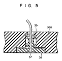
- a press-packed semiconductor device assembly comprising a heat discharging support member, and at least one semiconductor device including a semiconductor element having first, second and third electrodes, the first electrode positioned on one side of the semiconductor device and the second and the third electrodes positioned on the other side of the semiconductor device, the assembly including for each semiconductor device: a parallel pair of connection plates, embracing the semiconductor element; an electrode plate provided between one connection plate and the second electrode of the semiconductor element, the electrode plate having a through hole; a plurality of circuit elements mutually insulated and connected by said other connection plate; an insulating plate provided between the support member and the other connection plate; first pressing means for elastically pressing said one connection plate onto the electrode plate to electrically connect said one connection plate to the second electrode through the electrode plate and to connect the first electrode electrically to the other connection plate; a first connection member extending through the through hole in the electrode plate and contacting the third electrode; second pressing means mounted in the through hole in the electrode plate for elastically pressing one end portion of the connection member onto the third electrode
- numeral 31 denotes a heat-discharging substrate which is made of a high thermal conductive metal, such as cast aluminum.
- a ceramic substrate 32 which is electrically insulated and is common to semiconductor elements 35 (to be described later).
- Two collector electrodes 33a and 33b made of, for example, copper are arranged on the ceramic substrate 32 at predetermined positions, respectively (see Fig. 4).
- the collector electrode 33a has an external connection terminal 34a bent perpendicular to the pressing surface A of the collector electrode 33a.
- the collector electrode 33b also has an external connection terminal 34b bent perpendicular to the pressing surface A of the collector electrode 33b.
- an insulation member 46a resistant to spring force and a spring mechanism which comprises a cup spring 47a assembled in the insulation member 46a and a metal fixing plate 48a.
- an insulation member 46b resistant to the force of a spring and a spring mechanism which comprises a cup spring 47b assembled in the insulation member 46b, and a metal fixing plate 48b.
- the metal fixing plates 48a, 48b are fixed to the heat-discharging substrate 31 by bolts 49a and 49b, respectively. This arrangement permits the resilient force of the cup springs 47a, 47b to press the individual electrodes, semiconductor elements 35, ceramic substrate 32 and heat-discharging substrate 31 against each other.
- the device thus arranged is protected by a gel material to prevent damage to the individual electrodes which may result from poor insulation.
- the heat-discharging substrate 31 is covered with a lid 52 made of, for example, epoxy resin.
- the space between the heat-discharging substrate 31 and the lid 52 is filled with an adhesive 53a, which is epoxy-resin-based, for example.
- an adhesive 53a which is epoxy-resin-based, for example.
- the adhesive 53a has a thermal expansion coefficient close to that of aluminum (Al) which is the material for the heat-discharging substrate 31.
- the adhesives 53b, 53c have a thermal expansion coefficient close to that of copper (Cu) which is the material for the external connection terminals 34a, 34b, 41a, 51a, 51b.
- the difference in the thermal expansion coefficient between the adhesive 53a and the adhesives 53b, 53c thermally increases the sealing effect.
- the lid 52 is also provided with a tube 54 for mixing nitrogen in the gel inside the lid 52 to form spaces. These spaces suppress the expansion of the gel due to the increase in temperature.
- the spring mechanisms comprising the cup springs 47a, 47b are mounted on the emitter electrodes 40a, 40b, respectively.
- the bolts 49a and 49b are separately fastened so that the two semiconductor elements 35, 35 can be evenly pressed by the spring mechanisms.
- the bolts 44 and nut 45 are fastened together at the grooves 43, 43 so as to electrically connect the internal connection terminal 42a of the collector electrode 33a and the internal connection terminal 42b of the emitter electrode 40b, thus forming the common electrode.
- two circuit elements a main transistor and a feedback diode, are assembled in a single semiconductor element 35 and the electrodes of the two elements are evenly pressed, thus applying pressure evenly.
- the transitor module has the common electrode of two semiconductor elements 35, 35 separated into the collector electrode 33a and the emitter electrode 40b. These electrodes respectively have internal connection terminals 42a and 42b arranged so as to face each other. This enables the emitter electrode 40b to slide in a direction perpendicular to the surface A. As a result, after the collector electrode 33a and the emitter electrode 40b are separately pressed, the internal connection terminals 42a, 42b are fastened with the bolt 44 and nut 45 to make those electrodes a common electrode. Therefore, the individual electrodes of the two semiconductor elements 35, 35 can be pressed evenly and coupled together.
- the collector electrode 33a of one of the semiconductor elements 35, 35 is coupled to the emitter electrode 40b of the other semiconductor element 35 to form a common electrode, providing a series circuit arrangement.
- a parallel circuit arrangement merely requires that the emitter electrodes 40a and 40b should be coupled together to form the common electrode and should have internal connection terminals, respectively.
Landscapes
- Cooling Or The Like Of Semiconductors Or Solid State Devices (AREA)
- Die Bonding (AREA)
Claims (7)
- Assemblage à pression de dispositifs à semi-conducteur mis sous boîtier, comprenant un élément support (31) évacuant la chaleur, et au moins un dispositif à semi-conducteur incluant un élément semi-conducteur (35) ayant des première, deuxième et troisième électrodes, la première électrode étant placée sur un côté du dispositif à semi-conducteur et les deuxième et troisième électrodes étant placées sur l'autre côté du dispositif à semi-conducteur, l'assemblage incluant pour chaque dispositif à semi-conducteur :
une paire de plaques de connexion parallèle (33a, 40a, 33b, 40b), embrassant l'élément semi-conducteur ;
une plaque électrode (36a, 36b) disposée entre une plaque de connexion (40a, 40b) et la deuxième électrode de l'élément semi-conducteur, la plaque électrode comportant un trou traversant ;
une pluralité d'éléments de circuits mutuellement isolés et reliés par l'autre plaque de connexion (33a, 33b) ;
une plaque isolante (32) disposée entre l'élément support (31) et l'autre plaque de connexion ;
un premier moyen à pression (47a, 47b) pour presser de façon élastique ladite une plaque de connexion (40a, 40b) sur la plaque électrode (36a, 36b) pour relier électriquement ladite une plaque de connexion à la deuxième électrode par l'intermédiaire de la plaque électrode et pour relier électriquement la première électrode à l'autre plaque de connexion ;
un premier élément de connexion (37) s'étendant dans le trou traversant la plaque électrode (36a, 36b) et contactant la troisième électrode ;
un second moyen à pression (39) monté dans le trou traversant la plaque électrode (36a, 36b) pour presser de façon élastique une partie extrémité de l'élément de connexion (37) sur la troisième électrode de l'élément semi-conducteur pour réaliser une connexion électrique ; et,
un second élément de connexion (34a, 34b, 41a) s'étendant à partir de chaque paire de plaques de connexion et passant à l'extérieur d'une enveloppe (52) pour les dispositifs à semi-conducteur disposés sur ledit élément support (31). - Assemblage à pression de dispositifs à semi-conducteur mis sous boîtier selon la revendication 1, dans lequel chacun desdits éléments de circuit comprend un transistor principal et une diode de roue libre, et dans lequel des éléments de circuit d'attaque sont raccordés à une partie de ladite autre plaque de connexion par un moyen différent dudit premier moyen à pression.
- Assemblage à pression de dispositifs à semi-conducteur mis sous boîtier selon la revendication 1, dans lequel au moins deux dispositifs à semi-conducteur sont prévus et dans lequel ladite plaque isolante (32) est disposée entre l'élément support (31) et l'autre plaque de connexion (33a, 33b) de chaque dispositif à semi-conducteur pour placer l'autre plaque de connexion respective dans le même plan.
- Assemblage à pression de dispositifs à semi-conducteur mis sous boîtier selon la revendication 1 ou 3, comprenant en outre un moyen (44, 45) pour connecter électriquement et mécaniquement l'autre plaque de connexion (33a) d'un dispositif à semi-conducteur à une plaque de connexion (40b) de l'autre dispositif à semi-conducteur de manière à pouvoir coulisser dans une direction perpendiculaire à la surface d'appui du premier moyen à pression (47a, 47b).
- Assemblage à pression de dispositifs à semi-conducteur mis sous boîtier selon la revendication 4, dans lequel ledit moyen de connexion comprend des fentes (43) formées dans les prolongements respectifs des plaques connectées et un assemblage par vis et écrou (44, 45) pour connecter les plaques.
- Assemblage à pression de dispositifs à semi-conducteur mis sous boîtier selon la revendication 5, dans lequel lesdits prolongements s'étendent perpendiculairement aux surfaces d'appui dudit premier moyen à pression.
- Assemblage à pression de dispositifs à semi-conducteur mis sous boîtier selon la revendication 2, dans lequel ledit élément support (31) est fait de métal ; ladite enveloppe (52) est faite de résine ; et dans lequel l'espace entre ledit élément support (31) et ladite enveloppe (52) et scellée par de la résine qui a un coefficient de dilatation thermique différent de celui de la résine pour sceller les espaces entre ladite enveloppe (52) et ledit second élément de connexion (34a, 34b, 41a).
Applications Claiming Priority (4)
| Application Number | Priority Date | Filing Date | Title |
|---|---|---|---|
| JP181286/83 | 1983-09-29 | ||
| JP58181284A JPS6074461A (ja) | 1983-09-29 | 1983-09-29 | 半導体装置 |
| JP58181286A JPS6074462A (ja) | 1983-09-29 | 1983-09-29 | 半導体装置 |
| JP181284/83 | 1983-09-29 |
Publications (3)
| Publication Number | Publication Date |
|---|---|
| EP0138048A2 EP0138048A2 (fr) | 1985-04-24 |
| EP0138048A3 EP0138048A3 (en) | 1986-12-30 |
| EP0138048B1 true EP0138048B1 (fr) | 1993-12-15 |
Family
ID=26500529
Family Applications (1)
| Application Number | Title | Priority Date | Filing Date |
|---|---|---|---|
| EP19840110766 Expired - Lifetime EP0138048B1 (fr) | 1983-09-29 | 1984-09-10 | Dispositif semi-conducteur dans un empaquetage à pression |
Country Status (3)
| Country | Link |
|---|---|
| US (1) | US4694322A (fr) |
| EP (1) | EP0138048B1 (fr) |
| DE (1) | DE3486256T2 (fr) |
Families Citing this family (26)
| Publication number | Priority date | Publication date | Assignee | Title |
|---|---|---|---|---|
| US4853762A (en) * | 1986-03-27 | 1989-08-01 | International Rectifier Corporation | Semi-conductor modules |
| DE3717489A1 (de) * | 1987-05-23 | 1988-12-01 | Asea Brown Boveri | Leistungshalbleitermodul und verfahren zur herstellung des moduls |
| JPH0693468B2 (ja) * | 1988-08-09 | 1994-11-16 | 株式会社東芝 | 圧接平型半導体装置 |
| DE3839383A1 (de) * | 1988-11-22 | 1990-05-23 | Semikron Elektronik Gmbh | Verfahren zum herstellen einer halbleiterbaueinheit und vorrichtung zur durchfuehrung des verfahrens |
| US4994890A (en) * | 1989-11-27 | 1991-02-19 | Snap-On Tools Corporation | Rectifier structure with individual links |
| US5038197A (en) * | 1990-06-26 | 1991-08-06 | Harris Semiconductor Patents, Inc. | Hermetically sealed die package with floating source |
| EP0513410B1 (fr) * | 1991-05-15 | 1993-12-15 | IXYS Semiconductor GmbH | Module semi-conducteur de puissance et procédé de fabrication d'un tel module |
| JPH04352457A (ja) * | 1991-05-30 | 1992-12-07 | Mitsubishi Electric Corp | 圧接型半導体装置及びその製造方法 |
| DE4130160A1 (de) * | 1991-09-11 | 1993-03-25 | Export Contor Aussenhandel | Elektronische schaltung |
| US5168425A (en) * | 1991-10-16 | 1992-12-01 | General Electric Company | Mounting arrangements for high voltage/high power semiconductors |
| JP2936855B2 (ja) * | 1991-12-26 | 1999-08-23 | 富士電機株式会社 | 電力用半導体装置 |
| JPH06120390A (ja) * | 1992-10-05 | 1994-04-28 | Fuji Electric Co Ltd | 樹脂封止形半導体装置の端子構造 |
| US5563447A (en) * | 1993-09-07 | 1996-10-08 | Delco Electronics Corp. | High power semiconductor switch module |
| US5539254A (en) * | 1994-03-09 | 1996-07-23 | Delco Electronics Corp. | Substrate subassembly for a transistor switch module |
| FR2732184B1 (fr) * | 1995-03-21 | 1997-04-30 | Asulab Sa | Module electrique de puissance |
| US6127727A (en) * | 1998-04-06 | 2000-10-03 | Delco Electronics Corp. | Semiconductor substrate subassembly with alignment and stress relief features |
| US5895974A (en) * | 1998-04-06 | 1999-04-20 | Delco Electronics Corp. | Durable substrate subassembly for transistor switch module |
| DE19903245A1 (de) * | 1999-01-27 | 2000-08-03 | Asea Brown Boveri | Leistungshalbleitermodul |
| DE60129146T2 (de) * | 2001-12-24 | 2007-12-13 | Abb Research Ltd. | Modulgehäuse und Leistungshalbleitermodul |
| DE102006006423B4 (de) * | 2006-02-13 | 2009-06-10 | Semikron Elektronik Gmbh & Co. Kg | Leistungshalbleitermodul und zugehöriges Herstellungsverfahren |
| DE102006006425B4 (de) * | 2006-02-13 | 2009-06-10 | Semikron Elektronik Gmbh & Co. Kg | Leistungshalbleitermodul in Druckkontaktausführung |
| DE112011105612B4 (de) * | 2011-09-13 | 2014-12-31 | Toyota Jidosha Kabushiki Kaisha | Halbleitermodul |
| JP2015138835A (ja) * | 2014-01-21 | 2015-07-30 | 株式会社東芝 | 半導体装置 |
| RU2693521C1 (ru) * | 2015-08-25 | 2019-07-03 | Инфинеон Текнолоджиз Биполар Гмбх Унд Ко Кг | Модуль силового полупроводникового элемента с образующей резервуар прижимной пластиной |
| JP7354550B2 (ja) * | 2019-02-08 | 2023-10-03 | 富士電機株式会社 | 半導体モジュールの外部接続部、半導体モジュール、外部接続端子、および半導体モジュールの外部接続端子の製造方法 |
| JP7334485B2 (ja) * | 2019-06-07 | 2023-08-29 | 富士電機株式会社 | 半導体モジュールの外部接続部、半導体モジュールの外部接続部の製造方法、半導体モジュール、車両、及び外部接続部とバスバーとの接続方法 |
Family Cites Families (8)
| Publication number | Priority date | Publication date | Assignee | Title |
|---|---|---|---|---|
| DE2337694C2 (de) * | 1973-07-25 | 1984-10-25 | SEMIKRON Gesellschaft für Gleichrichterbau u. Elektronik mbH, 8500 Nürnberg | Halbleitergleichrichteranordnung hoher Strombelastbarkeit |
| DE7512573U (de) * | 1975-04-19 | 1975-09-04 | Semikron Gesellschaft Fuer Gleichri | Halbleitergleichrichteranordnung |
| DE2728313A1 (de) * | 1977-06-23 | 1979-01-04 | Siemens Ag | Halbleiterbauelement |
| DE2942409A1 (de) * | 1979-10-19 | 1981-04-23 | Siemens AG, 1000 Berlin und 8000 München | Halbleiterbauelement mit mehreren halbleiterkoerpern |
| DE3005313C2 (de) * | 1980-02-13 | 1986-05-28 | SEMIKRON Gesellschaft für Gleichrichterbau u. Elektronik mbH, 8500 Nürnberg | Halbleiteranordnung |
| JPS5710959A (en) * | 1980-06-23 | 1982-01-20 | Mitsubishi Electric Corp | Semiconductor device |
| JPS5715452A (en) * | 1980-06-30 | 1982-01-26 | Mitsubishi Electric Corp | Transistor module |
| DE3274926D1 (en) * | 1981-05-12 | 1987-02-05 | Lucas Ind Plc | A multi-phase bridge arrangement |
-
1984
- 1984-09-10 DE DE84110766T patent/DE3486256T2/de not_active Expired - Fee Related
- 1984-09-10 EP EP19840110766 patent/EP0138048B1/fr not_active Expired - Lifetime
- 1984-09-13 US US06/650,107 patent/US4694322A/en not_active Expired - Lifetime
Also Published As
| Publication number | Publication date |
|---|---|
| EP0138048A2 (fr) | 1985-04-24 |
| DE3486256T2 (de) | 1994-05-11 |
| US4694322A (en) | 1987-09-15 |
| EP0138048A3 (en) | 1986-12-30 |
| DE3486256D1 (de) | 1994-01-27 |
Similar Documents
| Publication | Publication Date | Title |
|---|---|---|
| EP0138048B1 (fr) | Dispositif semi-conducteur dans un empaquetage à pression | |
| US5841064A (en) | Peltier module | |
| US8680666B2 (en) | Bond wireless power module with double-sided single device cooling and immersion bath cooling | |
| US4498120A (en) | Electrical sub-assembly having a lead frame to be compressed between a circuit board and heat sink | |
| US4907067A (en) | Thermally efficient power device package | |
| US7608917B2 (en) | Power semiconductor module | |
| CN1036043C (zh) | 电源模块 | |
| RU2309482C2 (ru) | Силовой полупроводниковый модуль | |
| US5747876A (en) | Semiconductor device and semiconductor module | |
| US4748538A (en) | Semiconductor module | |
| EP1104025B1 (fr) | Dispositif a semi-conducteur | |
| EP1193761A2 (fr) | Dispositif semi-conducteur comprenant un dispositif de connection intermédiaire | |
| JPH11330283A (ja) | 半導体モジュール及び大型半導体モジュール | |
| WO1999052147A1 (fr) | Connexion par fils d'un boitier de circuits integres sur un dissipateur de chaleur | |
| KR20010104308A (ko) | 파워 세미컨덕터 모듈 | |
| JPS61292949A (ja) | 電力用半導体モジユ−ル | |
| CN1311899A (zh) | 将集成电路封装固定到热沉上的容性安装装置 | |
| EP1466357B1 (fr) | Enveloppe montee sur une surface avec fond de plaquette espace de la carte de support | |
| US20230245948A1 (en) | Semiconductor device and manufacturing method thereof | |
| US6507108B1 (en) | Power semiconductor module | |
| US20020060371A1 (en) | High-power semiconductor module, and use of such a high-power semiconductor module | |
| JP2023085765A (ja) | 半導体装置及び半導体装置の製造方法 | |
| US7229855B2 (en) | Process for assembling a double-sided circuit component | |
| US20240213106A1 (en) | Semiconductor device | |
| US3375415A (en) | High current rectifier |
Legal Events
| Date | Code | Title | Description |
|---|---|---|---|
| PUAI | Public reference made under article 153(3) epc to a published international application that has entered the european phase |
Free format text: ORIGINAL CODE: 0009012 |
|
| 17P | Request for examination filed |
Effective date: 19840910 |
|
| AK | Designated contracting states |
Designated state(s): DE FR GB |
|
| PUAL | Search report despatched |
Free format text: ORIGINAL CODE: 0009013 |
|
| AK | Designated contracting states |
Kind code of ref document: A3 Designated state(s): DE FR GB |
|
| 17Q | First examination report despatched |
Effective date: 19890220 |
|
| GRAA | (expected) grant |
Free format text: ORIGINAL CODE: 0009210 |
|
| AK | Designated contracting states |
Kind code of ref document: B1 Designated state(s): DE FR GB |
|
| REF | Corresponds to: |
Ref document number: 3486256 Country of ref document: DE Date of ref document: 19940127 |
|
| ET | Fr: translation filed | ||
| PLBE | No opposition filed within time limit |
Free format text: ORIGINAL CODE: 0009261 |
|
| STAA | Information on the status of an ep patent application or granted ep patent |
Free format text: STATUS: NO OPPOSITION FILED WITHIN TIME LIMIT |
|
| 26N | No opposition filed | ||
| PGFP | Annual fee paid to national office [announced via postgrant information from national office to epo] |
Ref country code: GB Payment date: 19970901 Year of fee payment: 14 |
|
| PGFP | Annual fee paid to national office [announced via postgrant information from national office to epo] |
Ref country code: FR Payment date: 19970909 Year of fee payment: 14 |
|
| PGFP | Annual fee paid to national office [announced via postgrant information from national office to epo] |
Ref country code: DE Payment date: 19970919 Year of fee payment: 14 |
|
| PG25 | Lapsed in a contracting state [announced via postgrant information from national office to epo] |
Ref country code: GB Free format text: LAPSE BECAUSE OF NON-PAYMENT OF DUE FEES Effective date: 19980910 |
|
| GBPC | Gb: european patent ceased through non-payment of renewal fee |
Effective date: 19980910 |
|
| PG25 | Lapsed in a contracting state [announced via postgrant information from national office to epo] |
Ref country code: FR Free format text: LAPSE BECAUSE OF NON-PAYMENT OF DUE FEES Effective date: 19990531 |
|
| PG25 | Lapsed in a contracting state [announced via postgrant information from national office to epo] |
Ref country code: DE Free format text: LAPSE BECAUSE OF NON-PAYMENT OF DUE FEES Effective date: 19990701 |
|
| REG | Reference to a national code |
Ref country code: FR Ref legal event code: ST |