EP0067588A1 - Lasers à injection - Google Patents
Lasers à injection Download PDFInfo
- Publication number
- EP0067588A1 EP0067588A1 EP82302742A EP82302742A EP0067588A1 EP 0067588 A1 EP0067588 A1 EP 0067588A1 EP 82302742 A EP82302742 A EP 82302742A EP 82302742 A EP82302742 A EP 82302742A EP 0067588 A1 EP0067588 A1 EP 0067588A1
- Authority
- EP
- European Patent Office
- Prior art keywords
- substrate
- mesa
- nonplanar
- laser
- lstv
- Prior art date
- Legal status (The legal status is an assumption and is not a legal conclusion. Google has not performed a legal analysis and makes no representation as to the accuracy of the status listed.)
- Granted
Links
- 238000002347 injection Methods 0.000 title claims abstract description 37
- 239000007924 injection Substances 0.000 title claims abstract description 37
- 239000000758 substrate Substances 0.000 claims abstract description 111
- 239000004065 semiconductor Substances 0.000 claims abstract description 16
- 238000012423 maintenance Methods 0.000 claims abstract 2
- 238000000407 epitaxy Methods 0.000 claims description 2
- 239000000463 material Substances 0.000 claims description 2
- 239000000126 substance Substances 0.000 claims description 2
- 230000012010 growth Effects 0.000 abstract description 40
- 238000000927 vapour-phase epitaxy Methods 0.000 abstract description 6
- 229910001218 Gallium arsenide Inorganic materials 0.000 description 17
- 230000003287 optical effect Effects 0.000 description 14
- 238000000034 method Methods 0.000 description 13
- 238000005253 cladding Methods 0.000 description 10
- 238000004943 liquid phase epitaxy Methods 0.000 description 10
- 239000007789 gas Substances 0.000 description 9
- 238000001451 molecular beam epitaxy Methods 0.000 description 9
- 230000008569 process Effects 0.000 description 9
- 239000013078 crystal Substances 0.000 description 8
- 230000000694 effects Effects 0.000 description 6
- 238000004519 manufacturing process Methods 0.000 description 6
- 235000012431 wafers Nutrition 0.000 description 6
- 238000005229 chemical vapour deposition Methods 0.000 description 4
- 150000001875 compounds Chemical class 0.000 description 4
- 230000007423 decrease Effects 0.000 description 4
- 230000003247 decreasing effect Effects 0.000 description 4
- 230000033001 locomotion Effects 0.000 description 4
- LYCAIKOWRPUZTN-UHFFFAOYSA-N Ethylene glycol Chemical compound OCCO LYCAIKOWRPUZTN-UHFFFAOYSA-N 0.000 description 3
- 238000009792 diffusion process Methods 0.000 description 3
- 238000005530 etching Methods 0.000 description 3
- 238000001465 metallisation Methods 0.000 description 3
- 230000005855 radiation Effects 0.000 description 3
- 230000008859 change Effects 0.000 description 2
- 230000004907 flux Effects 0.000 description 2
- 238000002360 preparation method Methods 0.000 description 2
- 230000001902 propagating effect Effects 0.000 description 2
- 230000003595 spectral effect Effects 0.000 description 2
- 229910000980 Aluminium gallium arsenide Inorganic materials 0.000 description 1
- 101150072084 BCAM gene Proteins 0.000 description 1
- RYGMFSIKBFXOCR-UHFFFAOYSA-N Copper Chemical compound [Cu] RYGMFSIKBFXOCR-UHFFFAOYSA-N 0.000 description 1
- QAOWNCQODCNURD-UHFFFAOYSA-N Sulfuric acid Chemical compound OS(O)(=O)=O QAOWNCQODCNURD-UHFFFAOYSA-N 0.000 description 1
- 229910052782 aluminium Inorganic materials 0.000 description 1
- 229910052787 antimony Inorganic materials 0.000 description 1
- 229910052785 arsenic Inorganic materials 0.000 description 1
- 201000009310 astigmatism Diseases 0.000 description 1
- 230000008901 benefit Effects 0.000 description 1
- 229910052793 cadmium Inorganic materials 0.000 description 1
- 238000012512 characterization method Methods 0.000 description 1
- 238000003486 chemical etching Methods 0.000 description 1
- 238000010276 construction Methods 0.000 description 1
- 229910052802 copper Inorganic materials 0.000 description 1
- 239000010949 copper Substances 0.000 description 1
- 230000008878 coupling Effects 0.000 description 1
- 238000010168 coupling process Methods 0.000 description 1
- 238000005859 coupling reaction Methods 0.000 description 1
- 238000000151 deposition Methods 0.000 description 1
- 238000010586 diagram Methods 0.000 description 1
- 230000001747 exhibiting effect Effects 0.000 description 1
- 229910052733 gallium Inorganic materials 0.000 description 1
- -1 i.e. Substances 0.000 description 1
- 239000007943 implant Substances 0.000 description 1
- 238000002513 implantation Methods 0.000 description 1
- 229910052738 indium Inorganic materials 0.000 description 1
- 229910052745 lead Inorganic materials 0.000 description 1
- 230000000873 masking effect Effects 0.000 description 1
- 229910052751 metal Inorganic materials 0.000 description 1
- 239000002184 metal Substances 0.000 description 1
- 150000002739 metals Chemical class 0.000 description 1
- 239000000203 mixture Substances 0.000 description 1
- 230000004048 modification Effects 0.000 description 1
- 238000012986 modification Methods 0.000 description 1
- 229910052757 nitrogen Inorganic materials 0.000 description 1
- 230000003534 oscillatory effect Effects 0.000 description 1
- 229910052698 phosphorus Inorganic materials 0.000 description 1
- 229920002120 photoresistant polymer Polymers 0.000 description 1
- 230000009467 reduction Effects 0.000 description 1
- 230000010076 replication Effects 0.000 description 1
- 230000003362 replicative effect Effects 0.000 description 1
- 239000000243 solution Substances 0.000 description 1
- 238000001228 spectrum Methods 0.000 description 1
- 229910052718 tin Inorganic materials 0.000 description 1
- 238000007740 vapor deposition Methods 0.000 description 1
- 239000012808 vapor phase Substances 0.000 description 1
- 238000001947 vapour-phase growth Methods 0.000 description 1
- 229910052725 zinc Inorganic materials 0.000 description 1
Images




Classifications
-
- H—ELECTRICITY
- H01—ELECTRIC ELEMENTS
- H01S—DEVICES USING THE PROCESS OF LIGHT AMPLIFICATION BY STIMULATED EMISSION OF RADIATION [LASER] TO AMPLIFY OR GENERATE LIGHT; DEVICES USING STIMULATED EMISSION OF ELECTROMAGNETIC RADIATION IN WAVE RANGES OTHER THAN OPTICAL
- H01S5/00—Semiconductor lasers
- H01S5/20—Structure or shape of the semiconductor body to guide the optical wave ; Confining structures perpendicular to the optical axis, e.g. index or gain guiding, stripe geometry, broad area lasers, gain tailoring, transverse or lateral reflectors, special cladding structures, MQW barrier reflection layers
-
- H—ELECTRICITY
- H01—ELECTRIC ELEMENTS
- H01S—DEVICES USING THE PROCESS OF LIGHT AMPLIFICATION BY STIMULATED EMISSION OF RADIATION [LASER] TO AMPLIFY OR GENERATE LIGHT; DEVICES USING STIMULATED EMISSION OF ELECTROMAGNETIC RADIATION IN WAVE RANGES OTHER THAN OPTICAL
- H01S5/00—Semiconductor lasers
- H01S5/20—Structure or shape of the semiconductor body to guide the optical wave ; Confining structures perpendicular to the optical axis, e.g. index or gain guiding, stripe geometry, broad area lasers, gain tailoring, transverse or lateral reflectors, special cladding structures, MQW barrier reflection layers
- H01S5/22—Structure or shape of the semiconductor body to guide the optical wave ; Confining structures perpendicular to the optical axis, e.g. index or gain guiding, stripe geometry, broad area lasers, gain tailoring, transverse or lateral reflectors, special cladding structures, MQW barrier reflection layers having a ridge or stripe structure
- H01S5/223—Buried stripe structure
- H01S5/2232—Buried stripe structure with inner confining structure between the active layer and the lower electrode
-
- H—ELECTRICITY
- H01—ELECTRIC ELEMENTS
- H01S—DEVICES USING THE PROCESS OF LIGHT AMPLIFICATION BY STIMULATED EMISSION OF RADIATION [LASER] TO AMPLIFY OR GENERATE LIGHT; DEVICES USING STIMULATED EMISSION OF ELECTROMAGNETIC RADIATION IN WAVE RANGES OTHER THAN OPTICAL
- H01S5/00—Semiconductor lasers
- H01S5/20—Structure or shape of the semiconductor body to guide the optical wave ; Confining structures perpendicular to the optical axis, e.g. index or gain guiding, stripe geometry, broad area lasers, gain tailoring, transverse or lateral reflectors, special cladding structures, MQW barrier reflection layers
- H01S5/24—Structure or shape of the semiconductor body to guide the optical wave ; Confining structures perpendicular to the optical axis, e.g. index or gain guiding, stripe geometry, broad area lasers, gain tailoring, transverse or lateral reflectors, special cladding structures, MQW barrier reflection layers having a grooved structure, e.g. V-grooved, crescent active layer in groove, VSIS laser
-
- H—ELECTRICITY
- H01—ELECTRIC ELEMENTS
- H01S—DEVICES USING THE PROCESS OF LIGHT AMPLIFICATION BY STIMULATED EMISSION OF RADIATION [LASER] TO AMPLIFY OR GENERATE LIGHT; DEVICES USING STIMULATED EMISSION OF ELECTROMAGNETIC RADIATION IN WAVE RANGES OTHER THAN OPTICAL
- H01S5/00—Semiconductor lasers
- H01S5/20—Structure or shape of the semiconductor body to guide the optical wave ; Confining structures perpendicular to the optical axis, e.g. index or gain guiding, stripe geometry, broad area lasers, gain tailoring, transverse or lateral reflectors, special cladding structures, MQW barrier reflection layers
- H01S5/2054—Methods of obtaining the confinement
- H01S5/2059—Methods of obtaining the confinement by means of particular conductivity zones, e.g. obtained by particle bombardment or diffusion
-
- H—ELECTRICITY
- H01—ELECTRIC ELEMENTS
- H01S—DEVICES USING THE PROCESS OF LIGHT AMPLIFICATION BY STIMULATED EMISSION OF RADIATION [LASER] TO AMPLIFY OR GENERATE LIGHT; DEVICES USING STIMULATED EMISSION OF ELECTROMAGNETIC RADIATION IN WAVE RANGES OTHER THAN OPTICAL
- H01S5/00—Semiconductor lasers
- H01S5/20—Structure or shape of the semiconductor body to guide the optical wave ; Confining structures perpendicular to the optical axis, e.g. index or gain guiding, stripe geometry, broad area lasers, gain tailoring, transverse or lateral reflectors, special cladding structures, MQW barrier reflection layers
- H01S5/22—Structure or shape of the semiconductor body to guide the optical wave ; Confining structures perpendicular to the optical axis, e.g. index or gain guiding, stripe geometry, broad area lasers, gain tailoring, transverse or lateral reflectors, special cladding structures, MQW barrier reflection layers having a ridge or stripe structure
- H01S5/223—Buried stripe structure
- H01S5/2232—Buried stripe structure with inner confining structure between the active layer and the lower electrode
- H01S5/2234—Buried stripe structure with inner confining structure between the active layer and the lower electrode having a structured substrate surface
-
- H—ELECTRICITY
- H01—ELECTRIC ELEMENTS
- H01S—DEVICES USING THE PROCESS OF LIGHT AMPLIFICATION BY STIMULATED EMISSION OF RADIATION [LASER] TO AMPLIFY OR GENERATE LIGHT; DEVICES USING STIMULATED EMISSION OF ELECTROMAGNETIC RADIATION IN WAVE RANGES OTHER THAN OPTICAL
- H01S5/00—Semiconductor lasers
- H01S5/20—Structure or shape of the semiconductor body to guide the optical wave ; Confining structures perpendicular to the optical axis, e.g. index or gain guiding, stripe geometry, broad area lasers, gain tailoring, transverse or lateral reflectors, special cladding structures, MQW barrier reflection layers
- H01S5/22—Structure or shape of the semiconductor body to guide the optical wave ; Confining structures perpendicular to the optical axis, e.g. index or gain guiding, stripe geometry, broad area lasers, gain tailoring, transverse or lateral reflectors, special cladding structures, MQW barrier reflection layers having a ridge or stripe structure
- H01S5/223—Buried stripe structure
- H01S5/2232—Buried stripe structure with inner confining structure between the active layer and the lower electrode
- H01S5/2234—Buried stripe structure with inner confining structure between the active layer and the lower electrode having a structured substrate surface
- H01S5/2235—Buried stripe structure with inner confining structure between the active layer and the lower electrode having a structured substrate surface with a protrusion
-
- H—ELECTRICITY
- H01—ELECTRIC ELEMENTS
- H01S—DEVICES USING THE PROCESS OF LIGHT AMPLIFICATION BY STIMULATED EMISSION OF RADIATION [LASER] TO AMPLIFY OR GENERATE LIGHT; DEVICES USING STIMULATED EMISSION OF ELECTROMAGNETIC RADIATION IN WAVE RANGES OTHER THAN OPTICAL
- H01S5/00—Semiconductor lasers
- H01S5/20—Structure or shape of the semiconductor body to guide the optical wave ; Confining structures perpendicular to the optical axis, e.g. index or gain guiding, stripe geometry, broad area lasers, gain tailoring, transverse or lateral reflectors, special cladding structures, MQW barrier reflection layers
- H01S5/22—Structure or shape of the semiconductor body to guide the optical wave ; Confining structures perpendicular to the optical axis, e.g. index or gain guiding, stripe geometry, broad area lasers, gain tailoring, transverse or lateral reflectors, special cladding structures, MQW barrier reflection layers having a ridge or stripe structure
- H01S5/223—Buried stripe structure
- H01S5/2237—Buried stripe structure with a non-planar active layer
Definitions
- This invention relates to the injection lasers having active layers with a real refractive index waveguiding property due to a lateral spatial thickness variation (LSTV) profile thereof in the active region of their active layers with fabrication of these profiles created by vapor phase epitaxy employing semiconductor substrates with a nonplanar pattern in their surface.
- the LSTV profile may be abrupt or gradual, or combination thereof, depending on the nonplanar pattern geometry and growth parameters.
- this invention deals with the employment of nonplanar substrate patterns, such as. channels or mesas. of particular geometry that produce these profiles in the active layer of a multilayer semiconductor injection laser fabricated in metalorganic chemical vapor deposition (MO-CVD) or in molecular beam epitaxy (MBE). which have improved operating characteristics compared to previously known injection lasers with nonplanar active regions.
- MO-CVD metalorganic chemical vapor deposition
- MBE molecular beam epitaxy
- nonplanar A class of lasers incorporating a nonplanar region in the active layer have been termed "nonplanar", denoting that the active layer possesses a nonplanar active region formed during laser fabrication.
- This nonplanar region is conventionally formed via liquid phase epitaxy (LPE) by growth of semiconductor layers over a semiconductor substrate having associated with its top surface a channel or a mesa.
- LPE liquid phase epitaxy
- An example of a channelled substrate nonplanar laser (CSNP) is disclosed in U.S. Patent No. 3,978,428 and in German OLS2,716,750.
- MSNP mesa substrate nonplanar laser
- semiconductor injection lasers having a nonplanar active region which includes a lateral spatial variation in the active region thickness exhibit improved properties, such as low, threshold current, linear light output versus current characteristics and stable fundamental transverse mode control. These properties may be improved by selection of the proper spatial variation thickness and spatial variation rapidity.
- MBE molecular beam epitaxy
- MO-CVD metalorganic chemical vapor deposition
- LPE processes permit nonplanar variations in layer contours and thicknesses as desired.
- LPE growth of channelled substrate lasers produced curved contours and thickness variations in deposited layers on the substrate.
- MBE and MO-CVD processes characteristically do not produce the same type of growth variations. Depending upon deposit rate, flow rate, substrate temperature etc., the deposited layers or films tend to "match" the contour and shape of the substrate surface. It would be desirable to start with a substrate surface having a desired contour or taper adequate to replicate the desired variations in thickness and taper in sequentially grown layers. But, it is more practical to develop the desired taper and thickness variation during growth process, as done in the past with LPE relative to nonplanar substrate patterns, and obtain better accuracy and control in the desired contour and thickness variations that MBE and MO-CVD processes would provide.
- One manner of providing desired lateral spatial thickness variations in the active region in MO-CVD processing is the employment of apertured masks (either temporary or integral) during the growth process.
- the uniform depositing phenomena in MO-CVD is "interrupted" by the presence of the mask aperture producing a deposited layer through the mask aperture that varies laterally in spatial thickness.
- the epitaxial dcpositon of layers will tend to take on the geometric characterization of the substrate surface. If a channel or mesa is present in or on the substrate surface, the subsequently deposited MO-CVD layers will tend to take on the nonplanar profile of the channel or mesa. In the case of flat channel bottoms or mesa tops, it has been previously observed that the subsequently grown MO-CVD layers including the active layer will have corresponding flat regions, replicating the form of the nonplanar profile. See the Article entitled, "Singlc-longitudinal-mode CW Room-temperature Ga 1-x Al x As-GaAs Channel-guide Lasers Grown By Metalorganic Chcmical Vapor Deposition". R. D.
- desired active region profiles may be obtained in vapor phase epitaxy by growth over nonplanar patterns at the substrate surface producing the desired lateral spatial thickness variation (LSTV) profile depending on the size and shape of the nonplanar substrate patterns and certain growth parameters.
- LSTV lateral spatial thickness variation
- These patterns form abrupt LSTV profiles and gradual LSTV profiles. Combinations of these two different profiles are possible.
- Examples of nonplanar patterns are substrate channels and mesas used in the past in fabricating these nonplanar devices. The smaller patterns have been found to provide desirable slight LSTV profiles that provide better laser operating characterisitics, particularly, mode control.
- the desired abrupt or gradual LSTV profile in the active region can be produced in the vapor phase epitaxy by imposing limitations on the size of the nonplanar substrate pattern at the surface of the laser substrate, taking into consideration the thicknesses of the active layer and certain growth parameters, thereby optimizing these laser characteristics and operation.
- These profiles produced in the active region of the laser permit lowest order mode selection via a real refractive index waveguiding created by the profile in that region.
- an injection laser comprising a plurality of contiguous layers of semiconductor material deposited by MO-CVD on a semiconductor substrate wherein the substrate surface is provided a with nonplanar pattern, e.g. a mesa, channel, or a mesa within a channel with the pattern having a height limited to less than about 100 nm but greater that 5 nm.
- One of the layers of the laser forms an active layer with an active region for optical wave propagation under lasing conditions.
- the active region has a shape and contour reminiscent of the nonplanar substrate pattern and having the gradual lateral spatial thickness variation (LSTV), although comparatively very small or slight in total thickness change laterally across the active region.
- LSTV lateral spatial thickness variation
- the LSTV profile permits lowest order transverse mode selection via a real refractive index waveguiding active region.
- the desired LSTV profile can be produced in the vapor phase processing by imposing limitations on the size of the nonplanar substrate pattern at the surface of the laser substrate.
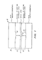
- Figure 1 illustrates a portion of a model injection laser 10 comprising a plurality of semiconductor layers. These lasers include an active layer 12 which provides optical wave propagation under lasing conditions as is well known in the art. For this illustration, regions 14 and 16 represent one or more cladding and intermediate semiconductor layers convcntional in the construction of these lasers.
- Active layer 12 has a nonplanar region 13 which is formed during MO-CVD or MBE growth due to a nonplanar pattern provided in the selected substrate 18 or 20.
- a nonplanar pattern provided in the selected substrate 18 or 20.
- Two different patterns are illustrated by substrates 18 and 20 but, in reality, only one such substrate would be employed in the fabrication process to form the nonplanar active region 13 while the other would represent the supcrstrate.
- the nonplanar pattern of substrate 18 is in the form of mesa 22, whereas the nonplanar pattern of substrate 20 is in the form of channel 24.
- Model laser 10 and subsequently described structures will be described in conjunction with elemental compounds used in fabricating GaAs/GaAlAs injection lascrs.
- other semiconductor matcrials forming elemental compounds made up of two or more elements from the group consisting of In, Ga, As, P, Sb, N, Al, Pb, Sn, Sc, Te, Cd and Zn may be employed in obtaining the desired profile in vapor phase epitaxy.
- Thin active regions with slight LSTV profiles are believed successful in MO-CVD because of the thinness of the active layer grown, the dimensions of the nonplanar pattern and responsible growth parameters. These intertwined growth parameters make it difficult to understand and describe precisely the optimum growth conditions. The extent of what is known now is given relative to the following parameters. Several parameters are to be considered.
- Substrate temperature The higher the temperature of the substrate, the more the tendency of the layer being deposited to form a facet along a given growth plane.
- the vapor phase growth is best carried out at atmospheric pressure so that the gases introduced into the MO-CVD reactor have a sufficient degree of random motion to cause initially larger deposits of elemental compounds in regions of comers or edges of nonplanar patterns due to substrate regional temperature differences.
- Substrate temperature gradient over the substrate i.e., substrate temperature differences between various substrate regions, possibly influenced by the turbulent effect created on gases flowing over and around substrate edges and nonplanar regions.
- Variation of gas flux density over nonplanar regions of the substrate This can be created by variations in the gas flow rates through the MO-CVD reactor.
- the growth plane which includes the nonplanar substrate pattern, is made to be transverse to the crystalographic orientation of the substrate.
- the substrate surface may be lapped at a very small angle, such as, one degree, and subsequently vapor deposited compounds on the transverse nonplanar substrate surface will tend to favor the crystalographic orientation resulting in spatial thickness variation in layers grown over the nonplanar pattern.
- Nonplanar substrate pattern misorientation The orientation of the pattern may be slightly misoricnted relative to the growth plane of the substrate.
- Nonplanar injection lasers processed in MO-CVD may be provided with what is term eo either an abrupt LSTV profile or a gradual LSTV profile or a combination of both. These profiles provide an abrupt thickness variation or a gradual thickness variation, which either separately or in combination, produce an effective, though small, lateral refractive index variation within the active region that improve the waveguiding characteristics and single mode operation of the laser.
- Figure 2A illustrates an abrupt profile 23.
- the ends of the cavity forming the limits of the active region 13 have a transverse index guiding edge or wall 25.1 and slightly thinner transverse region 25.2 that provide real index waveguiding for radiation propagating in the cavity of the active region.
- Walls 25 need only extend a short distance to function in index guiding propagating radiation.
- the height of the nonplanar substrate pattern be less than or on the order of the thickness of the active region 13.
- the height of the pattern e.g. a substrate mesa
- the thickness of the active region exceeds the thickness of the active region, undesirable higher order transverse modes have been observed.
- the optical wave intensity perpendicular to the plane of the p-n junction spreads substantially into the adjacent cladding layers. This spread of the optical wave intensity allows for a somewhat larger substrate pattern height or width to be used in order to still maintain fundamental mode operation.
- a 50 nm active layer thickness might utilize a 4 um wide by 200 nm high substrate pattern.
- Figures 2B illustrates a gradual LSTV profile.
- a gradual convex shaped LSTV profile 26 is illustrated.
- the thickest portion of the active region 13 is central and the spatial thickness decreases toward the ends of the region.
- Figures 2C, 2D and 2E illustrate combinations of the abrupt and gradual spatial thickness variation in the same profile.
- a gradual concave shaped LSTV profile 27 is illustrated.
- the thickest portions of the active region 13 are at region ends and the spatial thickness decreases toward the center of the region.
- the LSTV profile 29 is convex shaped with a spatial thickness variation through the active region as well as having thinner transverse regions 29.1 to provide real index waveguiding.
- the spatial variation is very small, being less than tens of nm from the thickest point to the thinnest point of the active region 13.
- the better examples having desired LSTV profiles thus far fabricated have shown desirable nonplanar patterns of about 2-6 J im wide with a pattern height between 20 to 50 nm.
- the active region 13 in such cases will be less than about 3 ⁇ m above the substrate and have a thickness of less than 400 nm at thickest point, for example, about 0.05 to 0.03 ⁇ m with a spatial thickness variation from the maximum to minimum of about 2 to 60 nm. With such small dimensions, it is very difficult to discern the exact nature of the gradual LSTV profile of the active region 13. However, the LSTV profile is present, whatever its contour, as explained later relative to the example set in Figures 7 et seq.
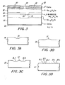
- laser 30 is a channelled substrate nonplanar laser of conventional design except being grown in MO-CVD with small channel geometry.
- Laser 30 comprises a substrate 32 of n-GaAs, cladding layer 34 of n-Ga 1-y Al y As, an active layer 36 of n,p or undoped Ga l-x Al x As, a cladding layer 38 of Ga l- w Al w As and capping layer 40 of P + GaAs.
- the molar requirements for this and other embodiments is w, y> x.
- Current confinement is provided by proton or ion implanted regions 42 forming the current channel 44. Other conventional current confinement schemes may also be utilized in these laser structures.
- a metalization layer 46 provides for n side contact while a contact applied to the region of channel 44 provides for p side contact.
- a nonplanar pattern in the form of channel 31 is provided in the surface of substrate 32.
- Channel 31 is 25 nm deep.
- Layer 34 may be about 2.5 ⁇ m thick while active layer 36 has an active region 33 of about 0.2 ⁇ m thick and has an LSTV differential of less than 10 nm e.g.7 nm.
- the profile may be either of the profiles shown in Figures 2B or 2C.
- a deeper channel 31 of, for example, 500 nm and a 0.2 ⁇ m thick active region 33 can provide the abrupt LSTV profile 23 of Figure 2A.
- Figure 3A illustatcs a modified pattern for substrate channel 31.
- Concave channel 35 has a rounded channel bottom that may be produced by a controlled selective etch or multiple etchants. This rounded shape imposes on the LSTV profile a more lens like shaped contour, which is desirable in the LSTV profile.
- Channel 35 will provide for more uniformity of growth in the regions of these edges.
- a special selective etch may be used that will tend to round all the pattern edges, producing either a concave channel or convex mesa.
- An example of such an etch is H 2 SO 4 , H 2 O 2 and H 2 O mixed in a ratio of 5:1:1.
- a multiple step etch may be necessary to achive the desired substrate surface contour.
- the resultant LSTV profile in the active region will depend considerably on the growth rate, growth temperature, and gas flow rates in the MO-CVD reactor as well as the overall dimensions of the rounded substrate pauern employed.
- Figure 3B illustrates a modified substrate pattern comprising a convex curved mesa 37.
- Figure 3C illustrates the employment of curved concave channels 35.1 and 35.2 in the substrate 32.
- Figure 3D illustrates that an array of several channels 35.1, 35.2, 35.n ( or mesas 37.1 to 37.n) may be closely spaced to provide for optical coupling among an array of active regions formed on substrate 32.
- Figure 3E illustrates an injection laser structure grown in MO-CVD employing a substrate 32 disclosed in Figure 3C.
- the laser 30' comprises the same semiconductor layers of laser 30 of Figure 3. Conventional means for current confinement and contact metalization are not shown. To be noted is the fairly uniform thickness of layer growth over the concave channels 35.1 and 35.2 and the convex mesa 37.1. However, for very thin layers, such as active layer 36 in the active regions 33, the LSTV profile will be produced, these profiles being shown somewhat exaggerated in this Figure for purpose of clarity.
- the injection laser 50 shown in Figure 4 illustrates a substrate 52 provided with a nonplanar pattern comprising a substrate channel 54 within which is formed a mesa 56.
- This configuration can be conventionally fabricated by selective etching.
- Conventional current confinement and contact metalization arc not shown.
- the diffused or grown regions 66 of p-GaAs on substrate 52 arc optional and provide reverse junction regions to confine current through the region of mesa 56. This technique is known in the art.
- the width of channel 54 may be, for example, 15 ⁇ m and mesa 56 may be about 6 ⁇ m wide and 25 nm high.
- MO-CVD growth with this mesa/channel geometry provides a gradual LSTV profile similar to Figures 2B and 2C for thin active regions 61, for example, less than 0,5 ⁇ m in height.
- the rapidity of the LSTV can be increased or decreased by increases or decreases in the depth of the channel 54 and the proximity of the adjacent mesas represented by surfaces 67.
- Active regions 61 with larger thicknesses will tend to flatten out and become linear without any LSTV profile sufficient (if at all present) to perform the desired real refractive index guiding function.
- active layers 61 with similar thicknesses deposited on higher mesas 57 will produce the abrupt LSTV profile 23 shown in Figure 2A. Active region 61 is applicable to all the profiles shown in the Figure 2 illustrations.
- a modification of laser 50 would be to make the height of the substrate surfaces 67 either higher or lower compared to the height 57 of mesa surface 57. These changes in height will have a resultant effect on the LSTV profile of region 61.
- An increase in height of surfaces 67 relative to mesa surface 57 will increase the differential amount of the LSTV as well as the overall region thickness for a given growth rate.
- a decrease in height of surfaces 67 relative to mesa surface 57 will reduce the differential amount of the LSTV as well as the overall region thickness for the same given growth rate.
- FIGS 5 and 6 illustrate exaggerated profile details in connection with injection laser 70 comprising substrate 72 of n-GaAs having a mesa 73, cladding layer 74 of n-Ga 1-y Al y As, active layer 76 of n, p or undoped GaAs or Ga 1-x Al x As, cladding layer 78 of p-Ga 1-w Al w As and capping layer 80 of p + -GaAs with proton implant regions 82 to form the current confinement channel 84. Contacts are not shown. In each of the Figures, the LSTV profile is quite different from that shown in Figure 2 but the resultant effect relative real refractive index waveguiding and mode control is the same.
- the LSTV profile in the active region 77 is in the form of a taper being of larger thickness at one edge 79 of region 77 and tapering to its smallest thickness at the other edge 81 of region 77.
- Such an LSTV taper can be produced by relative rotation or linear movement (indicated by arrow 86 and previously mentioned) of substrate 72 in a direction transverse to the longitudinal extent of the mesa 73 and also at a transverse shear to the gas flow indicated by arrows 88.
- This transverse shear effect may be also produced in a MO-CVD horizontal reactor wherein the gases flow over and across the nonplanar substrate surface. In all these cases, region 77 will grow thicker at the leading edge 79.
- the current confinement channel 84 is formed to be offset and over the thickest portions of region 77 at edge 79.
- the same tapered LSTV profile is also formed in region 77 of laser 70 shown in Figure 5B.
- the edge 79 is the largest thickness of region 77 tapering to its smallest thickness at the other edge 81 of region 77.
- This tapered LSTV profile is formed by a slight misorientation of the single crystal substrate relative to the longitudinal extent of the mesa 73.
- Substrate 72 may, for example, be misoriented one half of a degree or more measured from a plane perpendicular to the length of mesa 73. Because of this misorientation, the deposited crystalline growth tries to grow back to a perfect crystalline orientation and in doing so creates a tapered contour across active region 77.
- the amount of taper formed will depend upon growth parameters as well as the amount of pattern misorientation and pattern dimensions.
- the current confinement channel 84 is formed to be offset and over the thickest portions of region 77 at edge 79.
- Figure 6 shows the active region profile 27 of Figure 2C.
- a pair of thicker regions 83 over the mesa edges 73.1 and 73.2 appear at each active region edge 79 and 81.
- the offset current confinement channel 84 positioned over one of the regions 83, will provide lowest order mode operation, the designated region performing the functional index waveguiding due to LSTV profile of the region 83. It is possible that these regions may be developed due to a rounding of the two edges of the meas 73 when etched in the substrate 72. Also these regions may be developed due to growth conditions and surface kinetics, in particular, flux variation densities, diffusion gradients and atomic surface mobility.
- the rcmaining figures relate to the fabrication in MO-CVD of nonplanar substrate injection lasers each having a mesa of the same small height but of several different mesa widths and whose operational characteristics are compared to a planar substrate laser produced from the same MO-CVD growth.
- FIG. 7 A schematic diagram of the mesa waveguide structure of each of these fabricated lasers 100 is shown in Figure 7.
- the mesa shape of the active region 107 which results after etching of the n-GaAs substrate prior to crystal growth, propagates up through the grown layers 104-110 as the MO-CVD process proceeds.
- the device characteristcs set forth below compel a conclusion that the active layer is not completely flat across the mesa region 107 but instead tapers slightly from a maximum thickness located laterally above the center of the mesa 103.
- transverse mode control and waveguiding in these lasers is believed to be provided by a LSTV profile in the form of a lens-like active region in contast to channel guide lasers grown by MO-CVD, which have been said to exhibit gain guiding characteristics due to bends or offsets in the active region 107 at the edges 109.
- a LSTV profile in the form of a lens-like active region in contast to channel guide lasers grown by MO-CVD, which have been said to exhibit gain guiding characteristics due to bends or offsets in the active region 107 at the edges 109.
- mesas of width, w, equal to 2, 4, 6 and 8 ⁇ m are formed on n-(100) GaAs:Si doped substrates 102 by using projection exposure of photo resist This procedure maintains accurate mesa widths.
- chemical etching with 1 HF:6 H 3 P0 4 :30 H 2 0 2 :120 ethylene glycol is used to delineate a shallow mesa 103.
- a major advantage of this particular solution is that its etch rate is very well controlled and thus gives reproducible mesa heights,- which is an important parameter in maintaining single transverse mode operation in these devices.
- the mesa waveguide lasers 100 described herein are grown atop 50 nmhigh mesas.
- the mesa pattern consists of adjacent strips 2, 4, 6 and 8 ⁇ m wide, oriented parallel to the [011] direction. Each strip is separated by 500 ⁇ m from an adjacent mesa on the same wafer and the pattern is repeated across the wafer.
- the laser 100 comprises: (1) n-GaAs buffer layer 105, about L2 ⁇ m thick, Se-doped about 1x10 18 cm -3 ; (2) cladding layer 104 of n-Ga 0.7 Al 0.3 As, about 2 ⁇ m thick, Sc-dopcd about 3x10 17 cm -3 ; (3) undopcd GaAs active layer 106 about 0.15 ⁇ m thick; (4) cladding layer 108 p-Ga 0.7 Al 0 .
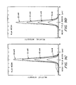
- L vs. I Pulsed light output vs. current (L vs. I) curves for MW lasers (labled “2, 4, 4, 6 and 8 ⁇ m MESA”) on a 275 ⁇ m long bar are depicted in Figure 8. Also shown is a typical L vs. I curve (labeled "NO MESA”) for a 4 ⁇ m wide stripe gain-guided injection laser approximately 275 ⁇ m long taken from a second wafer which was grown and processed simultaneously with the mesa lasers 100.
- the two wafers differ only in that one has mesas formed by etching the substrate prior to growth whereas the other substrate is featureless.
- the mesa laser thresholds are a factor of two lower than the 4 ⁇ m wide gain-guided featureless laser. This perhaps rather surprisingly large reduction in threshold is believed to result both from improved light guiding by the mesa waveguide and to enhanced charge diffusion toward the thickest part of the active region where the optical mode is the strongest. Both of these effects are a consequence of the LSTV profile of the active region.
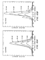
- the far field patterns of the mesa lasers 100 are shown in Figures 10A-10D, corresponding to the near field patterns of Figure9A-9D.
- the 10° full-width half-power (FWHP) far field divergence is consistent with a 2.0 ⁇ m FWHP planar Gaussian near field.
- Lasers similiar in design to laser 100, were also grown over 100, 200 and 400 nm high mesas. These devices operated in the lowest order transverse mode but at substantially lower output power levels, less than 3-5 mW. Above this power level, higher-order lateral modes were excited along the junction plane. With the larger mesa height, apparently, a large change in real refractive index weas induced, leading to high order mode operation. Thus, both mesa height and width are critical parameters in obtaining optimal laser performance from laser 100.
- Spectral purity continues to increase above threshold, as expected of a homogeneously broadened laser.
- the ratio of the intensity of the major longitudinal mode is approximately 180 times as intense as the adjacent longitudinal mode, which latter mode is second in intensity relative to the principle mode.
- the spectral purity is quite high, as is typical of real refractive index-guided lasers.
- active region profiles discussed can also be provided in multiple quantum well lasers, large optical cavity (LOC) lasers, buried heterostructure lasers and other known types of injection lasers.
- LOC large optical cavity
Landscapes
- Physics & Mathematics (AREA)
- Geometry (AREA)
- Condensed Matter Physics & Semiconductors (AREA)
- General Physics & Mathematics (AREA)
- Electromagnetism (AREA)
- Optics & Photonics (AREA)
- Semiconductor Lasers (AREA)
Applications Claiming Priority (2)
| Application Number | Priority Date | Filing Date | Title |
|---|---|---|---|
| US06/268,596 US4433417A (en) | 1981-05-29 | 1981-05-29 | Nonplanar substrate injection lasers grown in vapor phase epitaxy |
| US268596 | 1981-05-29 |
Publications (2)
| Publication Number | Publication Date |
|---|---|
| EP0067588A1 true EP0067588A1 (fr) | 1982-12-22 |
| EP0067588B1 EP0067588B1 (fr) | 1986-04-16 |
Family
ID=23023674
Family Applications (1)
| Application Number | Title | Priority Date | Filing Date |
|---|---|---|---|
| EP82302742A Expired EP0067588B1 (fr) | 1981-05-29 | 1982-05-27 | Lasers à injection |
Country Status (4)
| Country | Link |
|---|---|
| US (1) | US4433417A (fr) |
| EP (1) | EP0067588B1 (fr) |
| JP (1) | JPS57198690A (fr) |
| DE (1) | DE3270575D1 (fr) |
Cited By (1)
| Publication number | Priority date | Publication date | Assignee | Title |
|---|---|---|---|---|
| EP0143460A3 (en) * | 1983-11-30 | 1987-05-13 | Sharp Kabushiki Kaisha | Semiconductor laser device and production method thereof |
Families Citing this family (14)
| Publication number | Priority date | Publication date | Assignee | Title |
|---|---|---|---|---|
| US4623427A (en) * | 1983-08-12 | 1986-11-18 | Hewlett-Packard Company | Means and method for a self-aligned multilayer laser epitaxy structure device |
| JPS63166285A (ja) * | 1986-12-26 | 1988-07-09 | Toshiba Corp | 半導体発光装置の製造方法 |
| US5436192A (en) * | 1989-03-24 | 1995-07-25 | Xerox Corporation | Method of fabricating semiconductor structures via photo induced evaporation enhancement during in situ epitaxial growth |
| US4965806A (en) * | 1989-06-15 | 1990-10-23 | The United States Of America As Represented By The United States Department Of Energy | Semiconductor laser devices having lateral refractive index tailoring |
| US5048038A (en) * | 1990-01-25 | 1991-09-10 | The United States Of America As Represented By The United States Department Of Energy | Ion-implanted planar-buried-heterostructure diode laser |
| JPH04162689A (ja) * | 1990-10-26 | 1992-06-08 | Mitsubishi Electric Corp | 半導体発光装置の製造方法 |
| AU4104293A (en) * | 1992-05-19 | 1993-12-13 | California Institute Of Technology | Wide band-gap semiconductor light emitters |
| JPH07106701A (ja) * | 1993-10-05 | 1995-04-21 | Mitsubishi Electric Corp | 可視光半導体レーザ、及びその製造方法 |
| US6518168B1 (en) * | 1995-08-18 | 2003-02-11 | President And Fellows Of Harvard College | Self-assembled monolayer directed patterning of surfaces |
| US9310167B1 (en) * | 1995-11-28 | 2016-04-12 | Bae Systems Information And Electronic Systems Integration Inc. | Compact infrared countermeasure emitter |
| US6233264B1 (en) * | 1996-08-27 | 2001-05-15 | Ricoh Company, Ltd. | Optical semiconductor device having an active layer containing N |
| JP3459588B2 (ja) * | 1999-03-24 | 2003-10-20 | 三洋電機株式会社 | 半導体レーザ素子の製造方法 |
| US7269195B2 (en) * | 2002-03-04 | 2007-09-11 | Quintessence Photonics Corporation | Laser diode with an amplification section that has a varying index of refraction |
| JP4780993B2 (ja) * | 2005-03-31 | 2011-09-28 | 三洋電機株式会社 | 半導体レーザ素子およびその製造方法 |
Citations (2)
| Publication number | Priority date | Publication date | Assignee | Title |
|---|---|---|---|---|
| US3978428A (en) * | 1975-06-23 | 1976-08-31 | Xerox Corporation | Buried-heterostructure diode injection laser |
| EP0026062A1 (fr) * | 1979-09-12 | 1981-04-01 | Xerox Corporation | Laser semiconducteur à hétérojonction |
Family Cites Families (2)
| Publication number | Priority date | Publication date | Assignee | Title |
|---|---|---|---|---|
| JPS5521199A (en) * | 1978-07-31 | 1980-02-15 | Rca Corp | Semiconductor laser |
| US4215319A (en) * | 1979-01-17 | 1980-07-29 | Rca Corporation | Single filament semiconductor laser |
-
1981
- 1981-05-29 US US06/268,596 patent/US4433417A/en not_active Expired - Lifetime
-
1982
- 1982-05-20 JP JP57084122A patent/JPS57198690A/ja active Pending
- 1982-05-27 DE DE8282302742T patent/DE3270575D1/de not_active Expired
- 1982-05-27 EP EP82302742A patent/EP0067588B1/fr not_active Expired
Patent Citations (2)
| Publication number | Priority date | Publication date | Assignee | Title |
|---|---|---|---|---|
| US3978428A (en) * | 1975-06-23 | 1976-08-31 | Xerox Corporation | Buried-heterostructure diode injection laser |
| EP0026062A1 (fr) * | 1979-09-12 | 1981-04-01 | Xerox Corporation | Laser semiconducteur à hétérojonction |
Non-Patent Citations (1)
| Title |
|---|
| JANANESE JOURNAL OF APPLIED PHYSICS, vol. 19, Suppl. 19-1, 1980, pages 415-423, Tokyo (JP); * |
Cited By (2)
| Publication number | Priority date | Publication date | Assignee | Title |
|---|---|---|---|---|
| EP0143460A3 (en) * | 1983-11-30 | 1987-05-13 | Sharp Kabushiki Kaisha | Semiconductor laser device and production method thereof |
| US4937836A (en) * | 1983-11-30 | 1990-06-26 | Sharp Kabushiki Kaisha | Semiconductor laser device and production method therefor |
Also Published As
| Publication number | Publication date |
|---|---|
| DE3270575D1 (en) | 1986-05-22 |
| US4433417A (en) | 1984-02-21 |
| EP0067588B1 (fr) | 1986-04-16 |
| JPS57198690A (en) | 1982-12-06 |
Similar Documents
| Publication | Publication Date | Title |
|---|---|---|
| US4594718A (en) | Combination index/gain guided semiconductor lasers | |
| US4317085A (en) | Channeled mesa laser | |
| US4326176A (en) | Semiconductor laser device | |
| Simhony et al. | Vertically stacked multiple‐quantum‐wire semiconductor diode lasers | |
| US4371966A (en) | Heterostructure lasers with combination active strip and passive waveguide strip | |
| EP0002827B1 (fr) | Laser à hétérostructure à bande enterrée et son procédé de fabrication | |
| EP0132081B1 (fr) | Laser à semi-conducteur | |
| EP0067588B1 (fr) | Lasers à injection | |
| Kapon et al. | Patterned quantum well semiconductor injection laser grown by molecular beam epitaxy | |
| US4803691A (en) | Lateral superradiance suppressing diode laser bar | |
| JPH0656906B2 (ja) | 半導体レ−ザ装置 | |
| GB2046983A (en) | Semiconductor lasers | |
| US4270096A (en) | Semiconductor laser device | |
| EP0209387A2 (fr) | Dispositif laser à semi-conducteur | |
| US4868838A (en) | Semiconductor laser device | |
| US4752933A (en) | Semiconductor laser | |
| US4377865A (en) | Semiconductor laser | |
| EP0160490A2 (fr) | Laser à semi-conducteur | |
| EP0284684B1 (fr) | Laser à semi-conducteur avec canal inverse et substrat plan | |
| US4983541A (en) | Semiconductor laser device fabrication | |
| Scifres et al. | Mesa waveguide GaAs/GaAlAs injection laser grown by metalorganic chemical vapor deposition | |
| EP0298778B1 (fr) | Dispositifs de laser semi-conducteur et leur procédé de fabrication | |
| EP0396157B1 (fr) | Laser à semi-conducteur | |
| Zhu et al. | Low threshold ridge waveguide single quantum well laser processed by chemically assisted ion beam etching | |
| CA1125897A (fr) | Laser a heterostructure en microlignes plates enfouies |
Legal Events
| Date | Code | Title | Description |
|---|---|---|---|
| PUAI | Public reference made under article 153(3) epc to a published international application that has entered the european phase |
Free format text: ORIGINAL CODE: 0009012 |
|
| AK | Designated contracting states |
Designated state(s): DE FR GB |
|
| 17P | Request for examination filed |
Effective date: 19830609 |
|
| GRAA | (expected) grant |
Free format text: ORIGINAL CODE: 0009210 |
|
| AK | Designated contracting states |
Kind code of ref document: B1 Designated state(s): DE FR GB |
|
| REF | Corresponds to: |
Ref document number: 3270575 Country of ref document: DE Date of ref document: 19860522 |
|
| ET | Fr: translation filed | ||
| PLBE | No opposition filed within time limit |
Free format text: ORIGINAL CODE: 0009261 |
|
| STAA | Information on the status of an ep patent application or granted ep patent |
Free format text: STATUS: NO OPPOSITION FILED WITHIN TIME LIMIT |
|
| 26N | No opposition filed | ||
| PGFP | Annual fee paid to national office [announced via postgrant information from national office to epo] |
Ref country code: FR Payment date: 19990511 Year of fee payment: 18 |
|
| PGFP | Annual fee paid to national office [announced via postgrant information from national office to epo] |
Ref country code: GB Payment date: 19990526 Year of fee payment: 18 |
|
| PGFP | Annual fee paid to national office [announced via postgrant information from national office to epo] |
Ref country code: DE Payment date: 19990528 Year of fee payment: 18 |
|
| PG25 | Lapsed in a contracting state [announced via postgrant information from national office to epo] |
Ref country code: GB Free format text: LAPSE BECAUSE OF NON-PAYMENT OF DUE FEES Effective date: 20000527 |
|
| GBPC | Gb: european patent ceased through non-payment of renewal fee |
Effective date: 20000527 |
|
| PG25 | Lapsed in a contracting state [announced via postgrant information from national office to epo] |
Ref country code: FR Free format text: LAPSE BECAUSE OF NON-PAYMENT OF DUE FEES Effective date: 20010131 |
|
| PG25 | Lapsed in a contracting state [announced via postgrant information from national office to epo] |
Ref country code: DE Free format text: LAPSE BECAUSE OF NON-PAYMENT OF DUE FEES Effective date: 20010301 |
|
| REG | Reference to a national code |
Ref country code: FR Ref legal event code: ST |