EP0067969A2 - Steuerungsschaltung für thermischen Drucker - Google Patents
Steuerungsschaltung für thermischen Drucker Download PDFInfo
- Publication number
- EP0067969A2 EP0067969A2 EP82104514A EP82104514A EP0067969A2 EP 0067969 A2 EP0067969 A2 EP 0067969A2 EP 82104514 A EP82104514 A EP 82104514A EP 82104514 A EP82104514 A EP 82104514A EP 0067969 A2 EP0067969 A2 EP 0067969A2
- Authority
- EP
- European Patent Office
- Prior art keywords
- ribbon
- signal
- contact
- zone
- drive circuit
- Prior art date
- Legal status (The legal status is an assumption and is not a legal conclusion. Google has not performed a legal analysis and makes no representation as to the accuracy of the status listed.)
- Granted
Links
Images

Classifications
-
- B—PERFORMING OPERATIONS; TRANSPORTING
- B41—PRINTING; LINING MACHINES; TYPEWRITERS; STAMPS
- B41J—TYPEWRITERS; SELECTIVE PRINTING MECHANISMS, i.e. MECHANISMS PRINTING OTHERWISE THAN FROM A FORME; CORRECTION OF TYPOGRAPHICAL ERRORS
- B41J2/00—Typewriters or selective printing mechanisms characterised by the printing or marking process for which they are designed
- B41J2/315—Typewriters or selective printing mechanisms characterised by the printing or marking process for which they are designed characterised by selective application of heat to a heat sensitive printing or impression-transfer material
- B41J2/32—Typewriters or selective printing mechanisms characterised by the printing or marking process for which they are designed characterised by selective application of heat to a heat sensitive printing or impression-transfer material using thermal heads
- B41J2/35—Typewriters or selective printing mechanisms characterised by the printing or marking process for which they are designed characterised by selective application of heat to a heat sensitive printing or impression-transfer material using thermal heads providing current or voltage to the thermal head
- B41J2/355—Control circuits for heating-element selection
-
- B—PERFORMING OPERATIONS; TRANSPORTING
- B41—PRINTING; LINING MACHINES; TYPEWRITERS; STAMPS
- B41J—TYPEWRITERS; SELECTIVE PRINTING MECHANISMS, i.e. MECHANISMS PRINTING OTHERWISE THAN FROM A FORME; CORRECTION OF TYPOGRAPHICAL ERRORS
- B41J2/00—Typewriters or selective printing mechanisms characterised by the printing or marking process for which they are designed
- B41J2/315—Typewriters or selective printing mechanisms characterised by the printing or marking process for which they are designed characterised by selective application of heat to a heat sensitive printing or impression-transfer material
- B41J2/32—Typewriters or selective printing mechanisms characterised by the printing or marking process for which they are designed characterised by selective application of heat to a heat sensitive printing or impression-transfer material using thermal heads
- B41J2/325—Typewriters or selective printing mechanisms characterised by the printing or marking process for which they are designed characterised by selective application of heat to a heat sensitive printing or impression-transfer material using thermal heads by selective transfer of ink from ink carrier, e.g. from ink ribbon or sheet
Definitions
- the subject invention relates to circuitry for energizing the printhead of an electrothermal printer.
- One class of thermal printers utilizes a ribbon that generates localized heat internally in response to electrical signals.
- the localized heat then serves to cause marks to be formed on a receiving medium.
- the electrical signals are applied by printhead electrodes wiping accross an outer layer of the ribbon that is characterized by a moderate resistivity. These signals migrate inwardly to a layer that is highly conductive (preferably an aluminium layer) with localized heating occurring in the process.
- the path for the signals is completed by a contact engaging the conducting layer (see, e.g. US-A-2,713,822) or, alternatively, is completed through the moderately conducting layer at a collection plate (see, e.g. US-A-3,744,611) where electrical contact is established.
- the signals provided at the electrodes of the printhead cause heating within the ribbon which, in turn, results in a mark being formed.
- the mark may be produced because of a thermal sensitivity of the paper itself or, as is also known, by a transfer of a portion of an outer thermally transferrable ink layer of the ribbon.
- a shortcoming of the constant-current approach to driving the printhead electrodes arises because individual gated drive circuits are provided for each electrode thereby increasing overall drive circuit complexity and energy consumption.
- the subject invention involves a recognition that a significant contributor to printing quality variations for resistive ribbon printers is the voltage drop in the signal return path that includes the "buried" highly conducting layer of the ribbon. Furthermore, it is recognized that a voltage corresponding essentially to a voltage at the burried conducting layer may be monitored at an electrical contact that engages the ribbon at the surface of the resistive outer layer if such a contact is used in conjunction with a high impedance monitoring circuit.
- a drive circuit for use in a printer of the kind in which a printhead including a set of electrodes wipes over an outer moderately resistive layer of a signal responsive thermal printing ribbon at a print zone characterized in that first contact means establishing electrical contact with said ribbon at a first contact zone spaced from said printhead in a first direction along the ribbon; a second contact means establishing electrical contact with said ribbon at a second contact zone spaced from said printhead in the ribbon direction opposite said first direction; high impedance buffer means connected to said second contact means for producing a buffered feedback signal representative of the electrical potential of said ribbon at said second contact zone; means for generating gating signals for coordinating the energization respective of said electrodes; energization signal means for generating a voltage signal at least in part in accordance with said buffered feedback signal; switching means for selectively applying said voltage signal to said electrodes as respective printing signals in accordance with said gating signals; and conducting means for providing a low impedance electrical connection between said first contact
- the bulk of the drive signal current flows in one direction along the ribbon away from the printhead and the monitoring contact site is located on the ribbon a spaced interval from the printhead in the opposite direction so that all of the potential drop resulting from the flow of printing current in the highly conducting layer is included in the monitored potential.
- the drive voltage supplied to the electrodes is modifed to reduce the sensibi- tivity of the printing process to the return path voltage drop.
- the feedback signal is preferably used to modify the applied drive voltage so as to effectively cancel out the return path voltage drop.
- the feedback circuit preferably operates on the supply voltage ahead of switching gates that select the respective electrodes so that only one drive signal source is required. Equal-sized resistors may be placed in series with the individual electrodes to encourage uniformity of current flow.
- the drive signal return contact comprises a conducting roller located on the ribbon takeup side of the printhead and the electrical contact for monitoring is a conducting roller located on the ribbon supply side of the printhead.
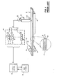
- a printhead 10 wipes or scans along a "resistive" ribbon 12 which is in contact with a receiving medium 14, such as paper, on which marks are formed.
- a set of printing electrodes 16 (a set of "N" electrodes is assumed in the discussion below) contact the resistive ribbon 12 at a printing zone, such contact occurring with the surface of a moderately resistive layer 18 (e.g. a resistance characteristic in a range of 200-400 ohms per square is preferred, but values over a greater range offer a possibility of satisfactory performance).
- Adjacent the resistive layer 18 is a thin conducting layer 20 which is preferably a thin layer of aluminium.
- An outer link layer 22 of thermally transferrable ink is typically formed adjacent to the conducting layer 20. However, if the receiving medium 14 is thermally sensitive, the outer link layer 22 is not required to form marks.
- printhead energization means 24 applies signals (denoted D 1 -D N ) to the printhead 10 through a set of electrode leads or channels 25 for causing mark formation on the receiving medium 14.
- signals denoted D 1 -D N
- a known way to achieve acceptably uniform printing quality involves the use of individual fixed- current drivers 26 (the current is denoted I K and the preferred direction of conventional current flow is indicated by an arrow) for the respective electrodes 16.
- the current drivers 26 are energized by a voltage source signal denoted Vs and are triggered by gating signals (denoted G 1 -G N ) to cause selective application of the signals D to the electrode 16.
- Signal D applied at the electrodes 16 tends to migrate through the moderately resistive layer 18 of the resistive ribbon 12 to the conducting layer 20 and cause localized heating in the process. Mark formation results from the localized heating either by a transfer of a portion of the ink layer 22 or by a change in the receiving medium 14 (e.g. with thermally sensitive paper).
- the signal path for the signals D extends predominantly through the conducting layer 20 to a collection zone where a collector contact 28 engages the ribbon 12.
- the collector contact 28 may be a conducting roller that engages the moderately resistive layer 18 and cooperates with a pressure roller 30 to achieve intimate electrical contact.
- the collector contacts 28 is electrically connected through a low-impedance connection 31 to provide for signal return path to the energization means 24.
- the low-impedance connection 31 may be a groun connection including portions of the printer frame (not shown) or a directly wired connection.
- the gating signals G that control the time intervals for the selective production of the signals D, are generated by a printer control 32 which cooperates with a font storage 34 as is well known for matrix printers. It should be appreciated that this arrangement requires individual current drivers 26 which provide a regulating action that involves significant heat generation.
- printhead energization means 24' receives a feddback signal S FBK from a monitor contact means 50 which is preferably an electrically conducting roller that cooperates with a pressure roller 52.
- the roller 50 is preferablly located on the path of the ribbon 12 at a position on the opposite side of the printhead 10 from the drive signal collector contact means 28. By so locating the monitoring point, it is possible to monitor a voltage level that is essentially the voltage of the conducting layer 20 at the printing zone (at the printhead 10), as is explained below.
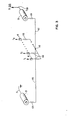
- a set of resistors 100 represent the path resistances between the electrodes 16 and the highly conducting layer 20.
- the resistance of the highly conducting layer 20 between the printing zone and the contact zone at the monitor contact means 50 is represented by a resistor 102 and a resistor 104 represents the resistance through the moderately resistive layer 18 to the monitor contact means 50.
- resistor 106 the resistance of the highly conducting layer section extending from the print zone to the contact zone for the contacting means 28.
- a resistor 108 represents the resistance through the moderately resistive layer 19 at the contact zone for the contact means 28. While it is possible as a consequence of the distributed nature of the ribbon resistances to identify other signal paths, they tend to be of less significance to the voltage levels of concern than those mentioned above.
- the current for the drive signals D would predominantly follow the path through the resistors 106 and 108 to the collector means 28 which offers a low impedance connection back to energization means 24'.
- This current flow for the drive signals D establishes a voltage at a node 110 which node essentially corresponds to the conducting layer 20 at the print zone. Since, for a high impedance connection to the connecting means 50, insignificant current would flow through the resistors 102 and 104 to produce a voltage drop, the voltage signal V FBK would essentially correspond to the voltage at the node 110.
- the contacting means 50 should be located on the ribbon path to allow monitoring the entire voltage drop from conducting layer 20 at the print zone through contact means 31 and back to energizing means 24'. This is best achieved by locating the monitor contact means 50 on the opposite side of the printhead 10 from the collector contact 28. It is preferred for the monitor contact means 50 to be on the supply side of the printhead 10 and the collector contact 28 on the takeup side, as is shown. Also, the monitor contact means 50 is spaced from the printhead 10 so that there is little or no contribution of potential resulting from migration of printing currents through the moderately conducting layer 18 that is added to the monitored potential.
- the signal S FBK from monitor contact means 50 is supplied to monitoring means 200, that is preferably an operational amplifier 202 in a connection with a pair of resistors 204 and 206 (presently preferred resistance values are indicated) to act as a high impedance analog buffer.
- a reference voltage V REF is supplied to an analog buffer 208 that is preferably an operational amplifier 210 in a connection with a pair of resistors 212. and 214 to act as a high impedance analog buffer.
- the signal V REF may be supplied by an operator adjustable potentiometer 215 but, alternatively, may be supplied by a controller such as a programmed microcomputer (not shown).
- Signals from monitoring means 200 and the buffer 208 are processed by means such as a summing circuit 216 which is preferably an operational amplifier 218 having connected at an input summing junction two input resistors 220 and 222 and a feedback resistor 224.
- the voltage from the buffer 200 serves as a buffered feedback, according to the invention, for cancelling all or a portion of the ribbon voltage transmitted to the monitor contact 50.
- the balance between the response to the signals S FBK and V REF is controlled by the relative sizes of the resistors 220 and 222 (for the presently preferred implementation equal resistances are used) and a multiplying effect on the sum is controlled by the sizing of the feedback resistor 224.
- the amplifier 218 serves as the single energy source providing an energization signal S E for a selection circuit 226 that includes a balancing resistor 228 and a signal controlled switching transistor 230 for each of the respective electrode channels 25.
- the balancing resistors serve to balance the flow of current among the channels 25 and the transistors 230 selectively switch drive signals D in accordance with the timed signals G which as was discussed above, are generated by a print control 32.
Landscapes
- Electronic Switches (AREA)
- Impression-Transfer Materials And Handling Thereof (AREA)
Applications Claiming Priority (2)
| Application Number | Priority Date | Filing Date | Title |
|---|---|---|---|
| US06/275,183 US4345845A (en) | 1981-06-19 | 1981-06-19 | Drive circuit for thermal printer |
| US275183 | 1988-11-23 |
Publications (3)
| Publication Number | Publication Date |
|---|---|
| EP0067969A2 true EP0067969A2 (de) | 1982-12-29 |
| EP0067969A3 EP0067969A3 (en) | 1985-04-17 |
| EP0067969B1 EP0067969B1 (de) | 1988-08-17 |
Family
ID=23051229
Family Applications (1)
| Application Number | Title | Priority Date | Filing Date |
|---|---|---|---|
| EP82104514A Expired EP0067969B1 (de) | 1981-06-19 | 1982-05-24 | Steuerungsschaltung für thermischen Drucker |
Country Status (5)
| Country | Link |
|---|---|
| US (1) | US4345845A (de) |
| EP (1) | EP0067969B1 (de) |
| JP (1) | JPS57212079A (de) |
| CA (1) | CA1162229A (de) |
| DE (1) | DE3278906D1 (de) |
Cited By (6)
| Publication number | Priority date | Publication date | Assignee | Title |
|---|---|---|---|---|
| EP0156111A1 (de) * | 1984-03-26 | 1985-10-02 | International Business Machines Corporation | Spannungsregelung bei angenähert konstanter Leistung für einen Wärmedruckkopf |
| EP0180049A3 (en) * | 1984-10-30 | 1987-01-14 | International Business Machines Corporation | Voltage mode printhead drive with sensing at the printhead |
| EP0098033B1 (de) * | 1982-06-29 | 1989-07-19 | Kabushiki Kaisha Toshiba | Thermodrucker mit Farbübertragung |
| EP0499373A3 (de) * | 1991-02-08 | 1992-08-26 | Hewlett-Packard Company | Energiesteuerungsschaltung für thermischen Tintenstrahldruckkopf |
| DE4221275A1 (de) * | 1992-06-26 | 1994-01-13 | Francotyp Postalia Gmbh | Ansteuerschaltung für eine elektrothermische Druckvorrichtung mit Widerstandsband |
| US6661840B1 (en) | 1999-04-23 | 2003-12-09 | Sony Corporation | Image encoder and method of the same |
Families Citing this family (21)
| Publication number | Priority date | Publication date | Assignee | Title |
|---|---|---|---|---|
| US4408908A (en) * | 1980-12-19 | 1983-10-11 | International Business Machines Corporation | Ribbon feed system for a matrix printer |
| JPS57189865A (en) | 1981-05-19 | 1982-11-22 | Ricoh Co Ltd | Recording method |
| GB2099763B (en) * | 1981-05-26 | 1985-12-04 | Ricoh Kk | Electrothermal non-impact recording method |
| US4384797A (en) * | 1981-08-13 | 1983-05-24 | International Business Machines Corporation | Single laminated element for thermal printing and lift-off correction, control therefor, and process |
| US4396308A (en) * | 1981-08-13 | 1983-08-02 | International Business Machines Corporation | Ribbon guiding for thermal lift-off correction |
| US4419024A (en) * | 1981-12-22 | 1983-12-06 | International Business Machines Corporation | Silicon dioxide intermediate layer in thermal transfer medium |
| US4421429A (en) * | 1981-12-22 | 1983-12-20 | International Business Machines Corporation | Resistive substrate for thermal printing ribbons comprising a mixture of thermosetting polyimide, thermoplastic polyimide, and conductive particulate material |
| JPS5971889A (ja) * | 1982-10-18 | 1984-04-23 | Tokyo Electric Co Ltd | サ−マルプリンタ |
| US4434356A (en) | 1982-12-22 | 1984-02-28 | International Business Machines Corporation | Regulated current source for thermal printhead |
| US4435634A (en) | 1982-12-22 | 1984-03-06 | International Business Machines Corporation | Thermal printer edge compensation |
| JPS6013571A (ja) * | 1983-07-04 | 1985-01-24 | Sony Corp | 印画装置 |
| GB2147763B (en) * | 1983-10-05 | 1987-03-04 | Suwa Seikosha Kk | Printing apparatus |
| JPS61202888A (ja) * | 1985-03-05 | 1986-09-08 | Sharp Corp | 記録方式 |
| US4603337A (en) * | 1985-03-28 | 1986-07-29 | Polaroid Corporation | Thermal transfer recording medium |
| US4556892A (en) * | 1985-03-28 | 1985-12-03 | Polaroid Corporation | Thermal transfer recording system and method |
| DE3868172D1 (de) * | 1987-07-31 | 1992-03-12 | Toshiba Kawasaki Kk | Elektrothermischer drucker mit einem widerstandsfarbband. |
| US5318369A (en) * | 1987-12-28 | 1994-06-07 | Kabushiki Kaisha Toshiba | Processing system with printer using exchangeable ink ribbon |
| US4929099A (en) * | 1988-01-19 | 1990-05-29 | Qume Corporation | Multi-line serial printer |
| DE4214545C2 (de) * | 1992-04-29 | 1996-08-14 | Francotyp Postalia Gmbh | Anordnung für eine ETR-Druckkopfansteuerung |
| EP0568162A1 (de) * | 1992-04-29 | 1993-11-03 | Francotyp-Postalia GmbH | Anordnung für eine ETR-Druckkopfansteuerung |
| DE19537161C1 (de) * | 1995-10-06 | 1996-12-19 | Francotyp Postalia Gmbh | Anordnung zur Überwachung der Funktion eines Tintendruckkopfes |
Family Cites Families (8)
| Publication number | Priority date | Publication date | Assignee | Title |
|---|---|---|---|---|
| US2713822A (en) * | 1948-12-20 | 1955-07-26 | Columbia Ribbon & Carbon | Planographic printing |
| US3132584A (en) * | 1954-07-26 | 1964-05-12 | Timefax Corp | Planographic master-forming blank and method of manufacture thereof |
| US3119919A (en) * | 1961-01-30 | 1964-01-28 | Daystrom Inc | Apparatus for the removal of portions of deposited metal films |
| DE2100611C3 (de) * | 1970-01-09 | 1978-05-03 | Ing. C. Olivetti & C., S.P.A., Ivrea, Turin (Italien) | Elektrothermische Druckvorrichtung |
| CH553065A (fr) * | 1972-04-26 | 1974-08-30 | Battelle Memorial Institute | Ruban a conductivite electrique anisotrope. |
| JPS511145A (en) * | 1974-06-21 | 1976-01-07 | Copal Co Ltd | Hatsushokunodono choseikanonakannetsukirokushikidentaku |
| US4032925A (en) * | 1976-05-10 | 1977-06-28 | Northern Telecom Limited | Drive circuit for thermal printing array |
| EP0028334A3 (de) * | 1979-11-01 | 1982-12-29 | International Business Machines Corporation | Verfahren und Vorrichtung, um Aufzeichnungsmaterial thermographisch zu bebildern |
-
1981
- 1981-06-19 US US06/275,183 patent/US4345845A/en not_active Expired - Lifetime
-
1982
- 1982-03-23 CA CA000399063A patent/CA1162229A/en not_active Expired
- 1982-04-09 JP JP57058346A patent/JPS57212079A/ja active Granted
- 1982-05-24 EP EP82104514A patent/EP0067969B1/de not_active Expired
- 1982-05-24 DE DE8282104514T patent/DE3278906D1/de not_active Expired
Non-Patent Citations (2)
| Title |
|---|
| IBM TECHNICAL DISCLOSURE BULLETIN, vol. 23, no. 9, February 1981, page 4302, New York, USA; C.V. WILBUR: "Thermal biasing technique for electrothermic printing" * |
| IBM TECHNICAL DISCLOSURE BULLETIN, vol. 23, no. 9, February 1981, pages 4305-4306, New York, USA; C.V. WILBUR: "Electrothermal print head" * |
Cited By (9)
| Publication number | Priority date | Publication date | Assignee | Title |
|---|---|---|---|---|
| EP0098033B1 (de) * | 1982-06-29 | 1989-07-19 | Kabushiki Kaisha Toshiba | Thermodrucker mit Farbübertragung |
| EP0156111A1 (de) * | 1984-03-26 | 1985-10-02 | International Business Machines Corporation | Spannungsregelung bei angenähert konstanter Leistung für einen Wärmedruckkopf |
| EP0180049A3 (en) * | 1984-10-30 | 1987-01-14 | International Business Machines Corporation | Voltage mode printhead drive with sensing at the printhead |
| EP0499373A3 (de) * | 1991-02-08 | 1992-08-26 | Hewlett-Packard Company | Energiesteuerungsschaltung für thermischen Tintenstrahldruckkopf |
| DE4221275A1 (de) * | 1992-06-26 | 1994-01-13 | Francotyp Postalia Gmbh | Ansteuerschaltung für eine elektrothermische Druckvorrichtung mit Widerstandsband |
| DE4342508A1 (de) * | 1992-06-26 | 1995-06-14 | Francotyp Postalia Gmbh | Ansteuerschaltung für eine elektrothermische Druckvorrichtung mit Widerstandsband, insbesondere Bandrißerkennung |
| US5482386A (en) * | 1992-06-26 | 1996-01-09 | Francotyp-Postalia Gmbh | Selection circuit for an electro-thermal printer with a resistance-type ribbon |
| EP0575668B1 (de) * | 1992-06-26 | 1997-03-12 | Francotyp-Postalia Aktiengesellschaft & Co. | Ansteuerschaltung für eine elektrothermische Druckvorrichtung mit Widerstandsband |
| US6661840B1 (en) | 1999-04-23 | 2003-12-09 | Sony Corporation | Image encoder and method of the same |
Also Published As
| Publication number | Publication date |
|---|---|
| JPS6257512B2 (de) | 1987-12-01 |
| EP0067969A3 (en) | 1985-04-17 |
| JPS57212079A (en) | 1982-12-27 |
| US4345845A (en) | 1982-08-24 |
| EP0067969B1 (de) | 1988-08-17 |
| CA1162229A (en) | 1984-02-14 |
| DE3278906D1 (en) | 1988-09-22 |
Similar Documents
| Publication | Publication Date | Title |
|---|---|---|
| US4345845A (en) | Drive circuit for thermal printer | |
| US4350449A (en) | Resistive ribbon printing apparatus and method | |
| US4434356A (en) | Regulated current source for thermal printhead | |
| US4531134A (en) | Regulated voltage and approximate constant power for thermal printhead | |
| HK69489A (en) | Printing apparatus | |
| US4425569A (en) | Non-impact recording method and apparatus | |
| EP0028334A2 (de) | Verfahren und Vorrichtung, um Aufzeichnungsmaterial thermographisch zu bebildern | |
| US4575731A (en) | Electro resistive printhead drive level sensing and control | |
| EP0113817B1 (de) | Randkompensation bei Thermodruckern | |
| US4217480A (en) | Thermal print bar | |
| JPS5814783A (ja) | 感熱記録装置の温度制御方式 | |
| EP0049100A3 (de) | Anschlagloser Drucker für Strichkodierungen und Methode zum Drucken von Strichkodierungen | |
| JPS58153676A (ja) | サ−マル転写印字装置 | |
| JP2528642Y2 (ja) | プリンタ装置 | |
| KR960010518B1 (ko) | 감열기록소자 | |
| JPH01225572A (ja) | 印写装置 | |
| JPH01198369A (ja) | 印写装置 | |
| JPH06416B2 (ja) | サーマルヘッドの抵抗値均一化方法 | |
| JPH0740571A (ja) | サーマルヘッド | |
| JPH02137940A (ja) | 印写装置 | |
| JPS60174666A (ja) | 印写装置 | |
| JPS59143660A (ja) | 感熱式プリンタ | |
| JPS63141765A (ja) | 感熱記録ヘツド | |
| JPS60147358A (ja) | 感熱記録装置 | |
| JPS62253471A (ja) | サ−マルプリンタの制御装置 |
Legal Events
| Date | Code | Title | Description |
|---|---|---|---|
| PUAI | Public reference made under article 153(3) epc to a published international application that has entered the european phase |
Free format text: ORIGINAL CODE: 0009012 |
|
| AK | Designated contracting states |
Designated state(s): DE FR GB IT |
|
| 17P | Request for examination filed |
Effective date: 19830420 |
|
| PUAL | Search report despatched |
Free format text: ORIGINAL CODE: 0009013 |
|
| AK | Designated contracting states |
Designated state(s): DE FR GB IT |
|
| 17Q | First examination report despatched |
Effective date: 19860527 |
|
| R17C | First examination report despatched (corrected) |
Effective date: 19870223 |
|
| GRAA | (expected) grant |
Free format text: ORIGINAL CODE: 0009210 |
|
| AK | Designated contracting states |
Kind code of ref document: B1 Designated state(s): DE FR GB IT |
|
| REF | Corresponds to: |
Ref document number: 3278906 Country of ref document: DE Date of ref document: 19880922 |
|
| ET | Fr: translation filed | ||
| ITF | It: translation for a ep patent filed | ||
| PLBE | No opposition filed within time limit |
Free format text: ORIGINAL CODE: 0009261 |
|
| STAA | Information on the status of an ep patent application or granted ep patent |
Free format text: STATUS: NO OPPOSITION FILED WITHIN TIME LIMIT |
|
| 26N | No opposition filed | ||
| REG | Reference to a national code |
Ref country code: FR Ref legal event code: GC |
|
| REG | Reference to a national code |
Ref country code: GB Ref legal event code: 732 |
|
| REG | Reference to a national code |
Ref country code: FR Ref legal event code: TP |
|
| ITPR | It: changes in ownership of a european patent |
Owner name: CESSIONE;LEXMARK INTERNATIONAL INC. |
|
| ITPR | It: changes in ownership of a european patent |
Owner name: PEGNO;J.P. MORGAN DELAWARE |
|
| ITTA | It: last paid annual fee | ||
| PGFP | Annual fee paid to national office [announced via postgrant information from national office to epo] |
Ref country code: FR Payment date: 19950411 Year of fee payment: 14 |
|
| PGFP | Annual fee paid to national office [announced via postgrant information from national office to epo] |
Ref country code: DE Payment date: 19950425 Year of fee payment: 14 |
|
| PGFP | Annual fee paid to national office [announced via postgrant information from national office to epo] |
Ref country code: GB Payment date: 19950428 Year of fee payment: 14 |
|
| PG25 | Lapsed in a contracting state [announced via postgrant information from national office to epo] |
Ref country code: GB Effective date: 19960524 |
|
| GBPC | Gb: european patent ceased through non-payment of renewal fee |
Effective date: 19960524 |
|
| PG25 | Lapsed in a contracting state [announced via postgrant information from national office to epo] |
Ref country code: FR Effective date: 19970131 |
|
| PG25 | Lapsed in a contracting state [announced via postgrant information from national office to epo] |
Ref country code: DE Effective date: 19970201 |
|
| REG | Reference to a national code |
Ref country code: FR Ref legal event code: ST |