EP0068185B1 - Circuit pour générer une tension continue de commande, dépendant d'une tension alternative - Google Patents
Circuit pour générer une tension continue de commande, dépendant d'une tension alternative Download PDFInfo
- Publication number
- EP0068185B1 EP0068185B1 EP82104967A EP82104967A EP0068185B1 EP 0068185 B1 EP0068185 B1 EP 0068185B1 EP 82104967 A EP82104967 A EP 82104967A EP 82104967 A EP82104967 A EP 82104967A EP 0068185 B1 EP0068185 B1 EP 0068185B1
- Authority
- EP
- European Patent Office
- Prior art keywords
- voltage
- circuit
- current
- fact
- transistor
- Prior art date
- Legal status (The legal status is an assumption and is not a legal conclusion. Google has not performed a legal analysis and makes no representation as to the accuracy of the status listed.)
- Expired
Links
Images


Classifications
-
- H—ELECTRICITY
- H02—GENERATION; CONVERSION OR DISTRIBUTION OF ELECTRIC POWER
- H02M—APPARATUS FOR CONVERSION BETWEEN AC AND AC, BETWEEN AC AND DC, OR BETWEEN DC AND DC, AND FOR USE WITH MAINS OR SIMILAR POWER SUPPLY SYSTEMS; CONVERSION OF DC OR AC INPUT POWER INTO SURGE OUTPUT POWER; CONTROL OR REGULATION THEREOF
- H02M7/00—Conversion of AC power input into DC power output; Conversion of DC power input into AC power output
- H02M7/02—Conversion of AC power input into DC power output without possibility of reversal
- H02M7/04—Conversion of AC power input into DC power output without possibility of reversal by static converters
- H02M7/12—Conversion of AC power input into DC power output without possibility of reversal by static converters using discharge tubes with control electrode or semiconductor devices with control electrode
- H02M7/21—Conversion of AC power input into DC power output without possibility of reversal by static converters using discharge tubes with control electrode or semiconductor devices with control electrode using devices of a triode or transistor type requiring continuous application of a control signal
-
- H—ELECTRICITY
- H03—ELECTRONIC CIRCUITRY
- H03G—CONTROL OF AMPLIFICATION
- H03G7/00—Volume compression or expansion in amplifiers
- H03G7/002—Volume compression or expansion in amplifiers in untuned or low-frequency amplifiers, e.g. audio amplifiers
Definitions
- the invention relates to a circuit arrangement for generating a control direct voltage dependent on an alternating voltage, as is reproduced in the preamble of claim 1.
- a short decay time is necessary to avoid audible noise plumes after the useful signal ends abruptly.
- a short decay time with a low-frequency useful signal leads to a high ripple in the control voltage and thus to signal distortion via the control.
- a long decay time is therefore necessary to avoid these signal distortions.
- a capacitor is charged via a current source.
- One input of a differential amplifier is connected to the capacitor, the other input to a reference voltage. Charging the capacitor initially causes a time delay. When the capacitor voltage finally reaches the level of the reference voltage, the differential amplifier is switched over very quickly. This happens in a range of approx. 50 mVolt. The switching of a control time constant caused by this circuit therefore takes place very quickly.
- the object of the invention is to reduce tolerance influences of the time-determining elements of the known circuit with little effort.
- the invention relates to the circuit arrangement reproduced in the preamble of claim 1.
- the stated object is achieved in such a circuit arrangement by the features reproduced in the characterizing part of claim 1.
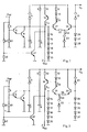
- the 1 shows the structure of a circuit according to the invention. It has an input 1 for the AC voltage U NF and an output 2 for the control DC voltage U ST .
- the input 1 controls the base of the transistors 5 and 6 connected as a Darlington circuit via a voltage divider 4, 40.
- the emitter of transistor 6 is at reference potential.
- the collectors of transistors 5 and 6 are connected to the first connections of current source 3, capacitor 7, diode path 15-20 and the base of transistor 21.
- the capacitor 7 and the diode path 15-20 are at the second connection at reference potential.
- the transistor 21 forms a differential amplifier with the transistor 24.
- the emitter of transistor 21 is connected via the negative feedback resistor 22 to the emitter of transistor 24 and the first connection of current source 23.
- the second connection of the current source 23 is at reference potential.
- the collector of transistor 24 is connected to the operating voltage U b .
- the base of the transistor 24 has a common contact with the diode path 26-28 and the current source 25.
- the second connection of the diode path leads to reference potential, the second connection of the current source 25 to the operating voltage U b .
- the collector of transistor 21 is connected to the base of transistor 11 and also to the operating voltage U b via the series connection of diode 13 and resistor 12.
- the emitter of the transistor 11 is connected to the operating voltage U b via the resistor 10.
- the transistors 5. 6 and 41 each set Threshold value switch represents: If the input voltage at input 1 exceeds a threshold value predetermined by the base-emitter voltage of transistor 41 and voltage divider 43, 42, the collector-emitter path of transistor 41 becomes conductive. As a result, the capacitor 8 is discharged through the collector-emitter resistance of the transistor 41 to more negative values and the output voltage at the terminal 2 becomes more negative. If the input voltage falls below the threshold value again, the transistor 41 is blocked again and the capacitor 8 is recharged to more positive values via the resistor 9. Thus the output voltage at 2 becomes more positive.
- the components 8, 9, 41, 42 represent a fast rectifier circuit, as described in DE-PS 2406258 Fig. 12 and DE-AS 24 03 799 Fig. 2.
- the takeover voltage range is equal to the product of the negative feedback resistor 22 and the current 1 23 .
- the current transfer through the transistor 21 is proportional to the capacitor voltage of the capacitor 7.
- the time of the current transfer is of the order of the time delay of the circuit.
- the increase in the current I 21 in the transistor 21 is supplied by the current mirror circuit, which consists of the resistors 10 and 12, the diode 13 and the transistor 11, to the capacitor 8 as current I 11 .
- the stream 1 11 is after
- 11max
- the constantly increasing current 1 11 rounds off the curve of the control voltage at output 2.
- FIG. 2 shows another embodiment of the circuit according to the invention.
- the negative feedback resistor 22 is omitted, but a negative feedback resistor 22 is eliminated, and a negative feedback resistor 38 is provided in the emitter branch of the transistor 24.
- the diode path 26-28! Is replaced by the diode path 33-37.
- the diode path at the base of the transistor 21 can also be replaced by a corresponding zener diode since it only serves to limit the voltage of the capacitor 7 above a value which is necessary for the current to be fully taken up by the transistor 21. It can also be omitted, then the voltage across the capacitor rises to the operating voltage.
- diode paths 26-28 and 33-37 and the current source 25 can be replaced by other suitable circuits which produce a substantially constant voltage at the base of the transistor 24.
- the current 1 21 begins to flow as soon as the capacitor voltage U 7 has reached the value of three diode voltages.
- the current 1 21 then increases proportionally to the capacitor voltage U 7 from zero to its maximum value.
- the resulting voltage curve at output 2 is shown in FIG. 3d.
- the control voltage U ST rises slowly. The increase is determined by the large time constant formed by capacitor 8 and resistor 9. After the holding time, the control voltage U ST is rounded.
- the current that is fed through the resistor 9 to the capacitor 8 is superimposed on the constant increasing current 1 11 , which is obtained by the current mirror circuit from the current 1 21 .
- the constantly increasing current 1 11 thus causes a curved, ie rounded, increase in the control voltage.
- the control voltage rises to its maximum value. If the control voltage is obtained in this way, then two rounded curves move against each other due to the tolerance influences specified above. The influence of this shift is smaller on average than in the previously known circuit.
- Fig. 4 shows a further embodiment. It is used as a peripheral circuit for the well-known HIGH-COM IC U401 B, here numbered 61, and also causes a rounding of the curve of the control voltage.
- the emitter of a transistor 52 is connected to a connecting terminal 44 of the IC 61, the emitter of a transistor 54 is connected via a resistor 12, the emitter of a transistor 11 is connected via a resistor 10, and a connection of a resistor 9 is connected.
- the second connection of the resistor 9 leads to the collector of the transistor 11, a connection of a capacitor 8 and an output 46 of the IC 61.
- An output 45 of the IC 61 is connected to the base of the transistor 52 and to a connection of a resistor 49.
- the other connection of the resistor 49 leads to the reference potential via the connection points with a resistor 50 and a capacitor 51.
- the resistor 50 and the capacitor 51 form a parallel connection.
- the common connection point leads on the one hand to reference potential, on the other hand it is connected to the collector of transistor 52, the base of transistor 54, the collector of transistor 54 and the base of transistor 11.
- the capacitor 8 connected to the output 46 of the IC 61 has its second connection at reference potential.
- the connection 47 of the IC's 61 is connected to reference potential.
- the connections 44 and 45 of the IC 61 have an internal switch 53 which is controlled by the signal voltage U NF .
- the switch 53 If there is a signal voltage U NF , the switch 53 is open, the signal voltage U NF falls below a threshold value (see DE-AS 28 50 736), the switch 53 is closed with a time delay caused by a circuit part in the IC 61 (see Scientific Reports, AEG-Telefunken 52 (1979) 1-2, p.103). Equivalent to the previous exemplary embodiments, the resistors 42, 43 and the transistor 41 are present in the internal circuit of the IC 61. The control voltage U ST is present at the terminal 46 of the IC 61.
- switch 53 is closed.
- the transistor 52 is thus opened and the capacitor 51 is connected to + Ub of the terminal 44.
- the transistor 11 is blocked, no current flows through the resistor 10 and transistor 11 to the capacitor 8.
- the switch 53 is closed with a time delay and the transistor 52 is thus also closed.
- the capacitor 51 now slowly discharges through the resistor 50.
- the latter slowly becomes conductive and a constantly increasing current flows through the resistance level 50 to ground. In the equilibrium state, a voltage is established across the capacitor 51, which is determined by the current flowing through the resistor 12, the transistor 13 and the resistor 50.
- the current rising until the equilibrium state is reached is supplied to the capacitor 8 through the current mirror circuit 10, 11, 12, 13.
- the voltage across capacitor 8 corresponds to control voltage U ST .
- the discharge circuit of the capacitor 8, consisting of the voltage divider 43, 42 and the transistor 41, is set so that it is driven by the peaks of the signal.
- the capacitor 8 is constantly charged by the current specified by the resistor 9.
Landscapes
- Engineering & Computer Science (AREA)
- Multimedia (AREA)
- Power Engineering (AREA)
- Amplifiers (AREA)
- Dc-Dc Converters (AREA)
- Rectifiers (AREA)
- Control Of Electrical Variables (AREA)
- Control Of Indicators Other Than Cathode Ray Tubes (AREA)
- Details Of Television Scanning (AREA)
- Polyesters Or Polycarbonates (AREA)
- Heterocyclic Carbon Compounds Containing A Hetero Ring Having Oxygen Or Sulfur (AREA)
- Charge And Discharge Circuits For Batteries Or The Like (AREA)
- Transition And Organic Metals Composition Catalysts For Addition Polymerization (AREA)
- Control Of Amplification And Gain Control (AREA)
- Liquid Crystal Substances (AREA)
- Measurement Of Force In General (AREA)
- Control Of El Displays (AREA)
- Power Steering Mechanism (AREA)
- Steering Control In Accordance With Driving Conditions (AREA)
- Control Of Eletrric Generators (AREA)
- Threshing Machine Elements (AREA)
- Adhesives Or Adhesive Processes (AREA)
- Apparatus For Radiation Diagnosis (AREA)
- Vehicle Body Suspensions (AREA)
- Burglar Alarm Systems (AREA)
- Hydraulic Clutches, Magnetic Clutches, Fluid Clutches, And Fluid Joints (AREA)
- Arrangement And Mounting Of Devices That Control Transmission Of Motive Force (AREA)
Claims (11)
Priority Applications (1)
| Application Number | Priority Date | Filing Date | Title |
|---|---|---|---|
| AT82104967T ATE11989T1 (de) | 1981-06-19 | 1982-06-07 | Schaltungsanordnung zur erzeugung einer von einer wechselspannung abhaengigen steuergleichspannung. |
Applications Claiming Priority (2)
| Application Number | Priority Date | Filing Date | Title |
|---|---|---|---|
| DE3124289 | 1981-06-19 | ||
| DE19813124289 DE3124289A1 (de) | 1981-06-19 | 1981-06-19 | Schaltungsanordnung zur erzeugung einer von einer wechselspannung abhaengigen steuergleichspannung |
Publications (2)
| Publication Number | Publication Date |
|---|---|
| EP0068185A1 EP0068185A1 (fr) | 1983-01-05 |
| EP0068185B1 true EP0068185B1 (fr) | 1985-02-20 |
Family
ID=6135013
Family Applications (1)
| Application Number | Title | Priority Date | Filing Date |
|---|---|---|---|
| EP82104967A Expired EP0068185B1 (fr) | 1981-06-19 | 1982-06-07 | Circuit pour générer une tension continue de commande, dépendant d'une tension alternative |
Country Status (18)
| Country | Link |
|---|---|
| US (1) | US4441041A (fr) |
| EP (1) | EP0068185B1 (fr) |
| JP (1) | JPS583005A (fr) |
| KR (1) | KR890002538B1 (fr) |
| AT (1) | ATE11989T1 (fr) |
| AU (1) | AU8477082A (fr) |
| BR (1) | BR8203523A (fr) |
| CA (1) | CA1174175A (fr) |
| DD (1) | DD210379A1 (fr) |
| DE (2) | DE3124289A1 (fr) |
| DK (1) | DK152471C (fr) |
| ES (1) | ES8304721A1 (fr) |
| FI (1) | FI73549C (fr) |
| NO (1) | NO822025L (fr) |
| PL (1) | PL236973A1 (fr) |
| SU (1) | SU1205792A3 (fr) |
| YU (1) | YU133282A (fr) |
| ZA (1) | ZA824161B (fr) |
Families Citing this family (4)
| Publication number | Priority date | Publication date | Assignee | Title |
|---|---|---|---|---|
| DE3305938A1 (de) * | 1983-02-21 | 1984-08-23 | Telefunken Fernseh Und Rundfunk Gmbh, 3000 Hannover | Schaltungsanordnung zur erzeugung einer von einer wechselspannung abhaengigen steuergleichspannung |
| JPH0368209A (ja) * | 1989-08-07 | 1991-03-25 | Fujitsu Ltd | 信号変換器 |
| US5065053A (en) * | 1990-02-26 | 1991-11-12 | Digital Equipment Corporation Of Canada, Ltd. | Exponential function circuitry |
| JP3319406B2 (ja) * | 1998-09-18 | 2002-09-03 | 日本電気株式会社 | 比較増幅検出回路 |
Family Cites Families (4)
| Publication number | Priority date | Publication date | Assignee | Title |
|---|---|---|---|---|
| US3371269A (en) * | 1964-05-18 | 1968-02-27 | Bendix Corp | Voltage regulator including means for eliminating ripple output voltages |
| NO142768C (no) * | 1974-01-26 | 1980-10-08 | Licentia Gmbh | Kopling for automatisk dynamikk-kompresjon eller -ekspansjon |
| DE2830784C3 (de) * | 1978-07-13 | 1981-10-01 | Licentia Patent-Verwaltungs-Gmbh, 6000 Frankfurt | Schaltungsanordnung zur Erzeugung einer von einer Wechselspannung abhängigen Steuergleichspannung |
| DE2850736C2 (de) * | 1978-11-23 | 1980-05-14 | Licentia Patent-Verwaltungs-Gmbh, 6000 Frankfurt | Schaltungsanordnung zur Erzeugung einer von einer Wechselspannung abhängigen Steuergleichspannung |
-
1981
- 1981-06-19 DE DE19813124289 patent/DE3124289A1/de not_active Withdrawn
-
1982
- 1982-06-01 DK DK246282A patent/DK152471C/da not_active IP Right Cessation
- 1982-06-07 AT AT82104967T patent/ATE11989T1/de active
- 1982-06-07 DE DE8282104967T patent/DE3262405D1/de not_active Expired
- 1982-06-07 EP EP82104967A patent/EP0068185B1/fr not_active Expired
- 1982-06-07 SU SU823449162A patent/SU1205792A3/ru active
- 1982-06-10 AU AU84770/82A patent/AU8477082A/en not_active Abandoned
- 1982-06-14 ZA ZA824161A patent/ZA824161B/xx unknown
- 1982-06-14 KR KR8202641A patent/KR890002538B1/ko not_active Expired
- 1982-06-16 BR BR8203523A patent/BR8203523A/pt unknown
- 1982-06-16 ES ES513144A patent/ES8304721A1/es not_active Expired
- 1982-06-17 PL PL23697382A patent/PL236973A1/xx unknown
- 1982-06-17 DD DD82240836A patent/DD210379A1/de unknown
- 1982-06-17 US US06/389,494 patent/US4441041A/en not_active Expired - Fee Related
- 1982-06-17 NO NO822025A patent/NO822025L/no unknown
- 1982-06-18 YU YU01332/82A patent/YU133282A/xx unknown
- 1982-06-18 CA CA000405477A patent/CA1174175A/fr not_active Expired
- 1982-06-18 FI FI822210A patent/FI73549C/fi not_active IP Right Cessation
- 1982-06-18 JP JP57104037A patent/JPS583005A/ja active Pending
Also Published As
| Publication number | Publication date |
|---|---|
| CA1174175A (fr) | 1984-09-11 |
| KR890002538B1 (ko) | 1989-07-13 |
| US4441041A (en) | 1984-04-03 |
| ES513144A0 (es) | 1983-03-16 |
| ZA824161B (en) | 1983-04-27 |
| BR8203523A (pt) | 1983-06-14 |
| ES8304721A1 (es) | 1983-03-16 |
| JPS583005A (ja) | 1983-01-08 |
| DD210379A1 (de) | 1984-06-06 |
| DE3262405D1 (en) | 1985-03-28 |
| NO822025L (no) | 1982-12-20 |
| DK152471B (da) | 1988-02-29 |
| DK152471C (da) | 1988-08-08 |
| EP0068185A1 (fr) | 1983-01-05 |
| FI822210A0 (fi) | 1982-06-18 |
| YU133282A (en) | 1985-04-30 |
| PL236973A1 (en) | 1983-01-31 |
| AU8477082A (en) | 1982-12-23 |
| FI73549C (fi) | 1987-10-09 |
| KR840001008A (ko) | 1984-03-26 |
| DE3124289A1 (de) | 1983-01-05 |
| SU1205792A3 (ru) | 1986-01-15 |
| FI822210L (fi) | 1982-12-20 |
| DK246282A (da) | 1982-12-20 |
| ATE11989T1 (de) | 1985-03-15 |
| FI73549B (fi) | 1987-06-30 |
Similar Documents
| Publication | Publication Date | Title |
|---|---|---|
| DE1095879B (de) | Transistor-Verzoegerungsstromkreis | |
| DE4430049C1 (de) | Schaltungsanordnung zur Unterspannungs-Erkennung | |
| DE2717059A1 (de) | Automatische verstaerkungs-steuerschaltung | |
| DE102019102535A1 (de) | Stromversorgungssteuereinrichtung | |
| EP0068185A1 (fr) | Circuit pour générer une tension continue de commande, dépendant d'une tension alternative | |
| DE2429374B2 (de) | Veraenderliche schwaechungsschaltung | |
| DE2842945B2 (de) | Schaltung zur Erzeugung eines Steuersignals zur Steuerung des Übertragungsmaßes von elektronisch steuerbaren Verstärkungs-oder Dämpfungsgliedern | |
| EP0309753A1 (fr) | Procédé de surveillance de charge inductive | |
| DE2137127A1 (de) | Schaltungsanordnung zur automatischen Verstärkungsregelung eines Signal verstärker s | |
| DE2427402A1 (de) | Stromversorgungsanordnung | |
| DE3113824C2 (de) | Verstärker mit Mitteln zum Unterdrücken von Gleichspannungssprüngen am Verstärkerausgang | |
| DE2938346C2 (de) | Stromversorgungsschaltung | |
| DE1524297C3 (de) | Driftkompensationsschaltung | |
| EP0264018A1 (fr) | Procédé de réglage d'ampfification dans des appareils téléphoniques à circuit de parole électronique et dispositif pour sa mise en application | |
| DE69700066T2 (de) | Regelvorrichtung einer Niederdruckleuchtstofflampe | |
| DE3740138C2 (fr) | ||
| DE2808707C2 (de) | Schaltungsanordnung zur Umschaltung zwischen Aufnahme und Wiedergabe bei einem Magnetbandgerät | |
| EP0495141B1 (fr) | Dispositif de réglage d'amplitude | |
| DE2359845C3 (de) | Schaltungsanordnung zur Konstanthaltung einer Gleichspannung | |
| DE2642948C3 (de) | Verfahren zur schnellen Einstellung des Arbeitsbereiches eines Transistorverstärkers | |
| DE3246944A1 (de) | Schaltungsanordnung zur ueberwachung einer elektrischen spannung | |
| DE2006757C3 (de) | Elektrische Schaltungsanordnung zur stufenlosen Veränderung der Nachstellzeitkonstanten eines Reglers mit nachgebender Rückführung | |
| DE2547804C3 (de) | Elektronischer Schalter für ein Wechselspannungssignal | |
| DE3011776C2 (de) | Verfahren zum automatischen Quittieren von Alarmanzeigelampen | |
| DE2917100C2 (de) | Ein-/Ausblendschaltung für einen NF-Verstärker |
Legal Events
| Date | Code | Title | Description |
|---|---|---|---|
| PUAI | Public reference made under article 153(3) epc to a published international application that has entered the european phase |
Free format text: ORIGINAL CODE: 0009012 |
|
| AK | Designated contracting states |
Designated state(s): AT BE CH DE FR GB IT LI LU NL SE |
|
| 17P | Request for examination filed |
Effective date: 19830622 |
|
| ITF | It: translation for a ep patent filed | ||
| GRAA | (expected) grant |
Free format text: ORIGINAL CODE: 0009210 |
|
| AK | Designated contracting states |
Designated state(s): AT BE CH DE FR GB IT LI LU NL SE |
|
| REF | Corresponds to: |
Ref document number: 11989 Country of ref document: AT Date of ref document: 19850315 Kind code of ref document: T |
|
| REF | Corresponds to: |
Ref document number: 3262405 Country of ref document: DE Date of ref document: 19850328 |
|
| ET | Fr: translation filed | ||
| PG25 | Lapsed in a contracting state [announced via postgrant information from national office to epo] |
Ref country code: LU Free format text: LAPSE BECAUSE OF NON-PAYMENT OF DUE FEES Effective date: 19850630 |
|
| BECH | Be: change of holder |
Free format text: 850220 *TELEFUNKEN FERNSEH UND RUNDFUNK G.M.B.H. |
|
| PLBE | No opposition filed within time limit |
Free format text: ORIGINAL CODE: 0009261 |
|
| STAA | Information on the status of an ep patent application or granted ep patent |
Free format text: STATUS: NO OPPOSITION FILED WITHIN TIME LIMIT |
|
| RAP2 | Party data changed (patent owner data changed or rights of a patent transferred) |
Owner name: TELEFUNKEN FERNSEH UND RUNDFUNK GMBH |
|
| 26N | No opposition filed | ||
| REG | Reference to a national code |
Ref country code: CH Ref legal event code: PUE Owner name: TELEFUNKEN FERNSEH UND RUNDFUNK GMBH |
|
| PGFP | Annual fee paid to national office [announced via postgrant information from national office to epo] |
Ref country code: AT Payment date: 19860611 Year of fee payment: 5 |
|
| NLS | Nl: assignments of ep-patents |
Owner name: TELEFUNKEN FERNSEH UND RUNDFUNK GMBH TE HANNOVER, |
|
| PGFP | Annual fee paid to national office [announced via postgrant information from national office to epo] |
Ref country code: NL Payment date: 19870630 Year of fee payment: 6 |
|
| PG25 | Lapsed in a contracting state [announced via postgrant information from national office to epo] |
Ref country code: GB Effective date: 19890607 Ref country code: AT Effective date: 19890607 |
|
| PG25 | Lapsed in a contracting state [announced via postgrant information from national office to epo] |
Ref country code: SE Effective date: 19890608 |
|
| PG25 | Lapsed in a contracting state [announced via postgrant information from national office to epo] |
Ref country code: LI Effective date: 19890630 Ref country code: CH Effective date: 19890630 Ref country code: BE Effective date: 19890630 |
|
| BERE | Be: lapsed |
Owner name: TELEFUNKEN FERNSEH UND RUNDFUNK G.M.B.H. Effective date: 19890630 |
|
| PG25 | Lapsed in a contracting state [announced via postgrant information from national office to epo] |
Ref country code: NL Effective date: 19900101 |
|
| GBPC | Gb: european patent ceased through non-payment of renewal fee | ||
| NLV4 | Nl: lapsed or anulled due to non-payment of the annual fee | ||
| PG25 | Lapsed in a contracting state [announced via postgrant information from national office to epo] |
Ref country code: FR Free format text: LAPSE BECAUSE OF NON-PAYMENT OF DUE FEES Effective date: 19900228 |
|
| REG | Reference to a national code |
Ref country code: CH Ref legal event code: PL |
|
| PG25 | Lapsed in a contracting state [announced via postgrant information from national office to epo] |
Ref country code: DE Effective date: 19900301 |
|
| REG | Reference to a national code |
Ref country code: FR Ref legal event code: ST |
|
| REG | Reference to a national code |
Ref country code: LU Ref legal event code: TP Owner name: TELEFUNKEN FERNSEH- UND RUNDFUNK GMBH HANNOVER Effective date: 19860327 |
|
| EUG | Se: european patent has lapsed |
Ref document number: 82104967.3 Effective date: 19900412 |