EP0264018A1 - Procédé de réglage d'ampfification dans des appareils téléphoniques à circuit de parole électronique et dispositif pour sa mise en application - Google Patents
Procédé de réglage d'ampfification dans des appareils téléphoniques à circuit de parole électronique et dispositif pour sa mise en application Download PDFInfo
- Publication number
- EP0264018A1 EP0264018A1 EP87114211A EP87114211A EP0264018A1 EP 0264018 A1 EP0264018 A1 EP 0264018A1 EP 87114211 A EP87114211 A EP 87114211A EP 87114211 A EP87114211 A EP 87114211A EP 0264018 A1 EP0264018 A1 EP 0264018A1
- Authority
- EP
- European Patent Office
- Prior art keywords
- signals
- ngs
- limit
- pgs
- voltage
- Prior art date
- Legal status (The legal status is an assumption and is not a legal conclusion. Google has not performed a legal analysis and makes no representation as to the accuracy of the status listed.)
- Withdrawn
Links
- 238000000034 method Methods 0.000 title claims description 17
- 230000003321 amplification Effects 0.000 title description 3
- 238000003199 nucleic acid amplification method Methods 0.000 title description 3
- 238000005259 measurement Methods 0.000 claims description 13
- 230000001419 dependent effect Effects 0.000 claims description 4
- 230000001105 regulatory effect Effects 0.000 claims description 4
- 239000003990 capacitor Substances 0.000 description 8
- 238000010586 diagram Methods 0.000 description 5
- 230000005540 biological transmission Effects 0.000 description 3
- 238000007493 shaping process Methods 0.000 description 2
- 230000033228 biological regulation Effects 0.000 description 1
- 230000007423 decrease Effects 0.000 description 1
- 230000003111 delayed effect Effects 0.000 description 1
- 238000001514 detection method Methods 0.000 description 1
- 230000002349 favourable effect Effects 0.000 description 1
Images
Classifications
-
- H—ELECTRICITY
- H04—ELECTRIC COMMUNICATION TECHNIQUE
- H04M—TELEPHONIC COMMUNICATION
- H04M1/00—Substation equipment, e.g. for use by subscribers
- H04M1/738—Interface circuits for coupling substations to external telephone lines
- H04M1/76—Compensating for differences in line impedance
-
- H—ELECTRICITY
- H04—ELECTRIC COMMUNICATION TECHNIQUE
- H04M—TELEPHONIC COMMUNICATION
- H04M1/00—Substation equipment, e.g. for use by subscribers
- H04M1/60—Substation equipment, e.g. for use by subscribers including speech amplifiers
- H04M1/6008—Substation equipment, e.g. for use by subscribers including speech amplifiers in the transmitter circuit
Definitions
- the invention relates to a method according to the preamble of claim 1 and an apparatus for performing the method.
- the invention has for its object to provide a method for gain control for telephones with electronic speech circuit, in which a signal limitation possible by overdriving is prevented.
- the invention is also based on the object of specifying a device for carrying out this method.
- the invention has the advantage that the maximum possible modulation range determined by the feed and load conditions can always be optimally used because the signal level cannot leave this range due to the regulation.
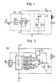
- FIG. 1 shows schematically the connection of a subscriber with a speech circuit arrangement SS1 via the connection terminals La and Lb to a telephone line for external power supply.
- FIG. 1 shows an asymmetrical feed and line representation.
- the speech circuit arrangement SS1 contains the microphone amplifier MV, which is connected on the input side to the microphone M via the microphone terminal Mk and which controls the modulation current source I1 on the output side.
- Parallel to I1 is the quiescent current source I01, through which a direct current required to maintain the functionality of the speech circuit arrangement SS1 flows.
- the speech circuit arrangement SS1 is connected to the office via a telephone line symbolized by the equivalent line resistance RL, which is represented by the supply voltage source UA and the inductance LA.
- Parallel to the series connection from UA, LA, RL is the network ZA, which symbolizes the impedance of the line which the speech circuit arrangement SS1 "sees" at the two terminals La, Lb.
- the impedance ZA contains the series circuit of a capacitor CA, a resistor R1 and a parallel circuit made up of the elements R2, C2. 1 means that the line resistance RL is only influenced by the direct current behavior of the arrangement and the capacitance CA means that the complex impedance ZA only affects the alternating current behavior of the arrangement.
- the size of the line current of the telephone line depends on the exchange voltage UA, the exchange resistance, the DC line resistance RL and the DC subscriber resistance.
- the modulation current source I1 drawn as a current sink Speech circuit arrangement SS1 generates a DC current value which corresponds to the difference between the line current of the telephone line and the quiescent current source I01.
- the modulation current source I1 is controlled by the microphone M or the microphone amplifier MV, an alternating current is superimposed on this direct current.
- the limits of the linear modulation range can be derived from the circuit diagram according to FIG. 1.
- the electronic speech circuit arrangement SS1 which generates the line signal as a sink current of the modulation current source I1 modulated by the microphone M, has reached the maximum value of the line signal when a further rise in voltage at the terminals La and Lb is no longer possible due to a reduction in the current through I1.
- This maximum value depends on the voltage of the voltage source UA and on the effective load impedance, which according to FIG. 1 is composed of the resistor RL and the impedance ZA.
- This limit value, at which the modulation current through I1 is zero in extreme cases, is referred to as a positive limit value.
- a second limit value which is referred to as a negative limit value, results from the fact that the electronic speech circuit arrangement SS1 requires a minimum voltage at its output terminals La and Lb, e.g. the saturation voltage of a transistor, which can fall below, for example, in the event of a voltage change on the telephone line.
- measurement signals and limit value signals are generated by an electronic speech circuit which characterize the current line signal and limit values for the modulation limits.
- the comparison of the signals is the gain of the microphone when the modulation limits are reached with the aid of a control device amplifier regulated back.
- the type of these signals ie whether current or voltage signals, and the way in which they are generated depend on the particular embodiment of the speech circuit arrangement; they can be produced using the means known in the art.
- the signals for the positive and negative limit values can be fixed or dependent on the current or voltage state of the telephone line if the limit values characterizing the modulation limits of the speech circuit arrangement are dependent on the current or voltage state of the telephone line.
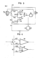
- a controllable microphone amplifier SMV connected on the input side to the microphone terminal Mk controls the modulation current source I1 on the output side.
- the modulation current source I1 is connected on the output side to terminals La and Lb for connection to the telephone line.
- the quiescent current source I01 is connected to the terminals La and Lb.
- signals S1 to S4 are derived from this modulation current source and brought out. After reshaping by the assigned signal processing devices SV1 to SV4, the signals S1 and S2 allow the negative limitation to be detected by the comparator or differential amplifier DN and the signals S3 and S4 to detect the positive limitation by the comparator or differential amplifier DP.
- This detection of the limitation takes place in that instantaneous line signals AS1 and AS2, which characterize the instantaneous electrical state of the modulation current source, are formed from the signals S1 and S3 by shaping, and that limit signals NGS and PGS are formed from the signals S2 and S4 after shaping, the the maximum characterize permitted states, ie they correspond to the negative or the positive limit value of the modulation range.
- the signals AS1 and NGS are now compared in the comparator DN and the signals AS2 and PGS in the comparator DP.
- the outputs of the two comparators DN and DP are fed to a control device which regulates the amplification of the controllable microphone amplifier SMV via an OR gate OR, a diode D and an actuator SG.
- the OR gate OR is controlled by the outputs of the two comparators DN and DP.
- a time delay element which, according to FIG. 2, can consist, for example, of a resistor RZ and a capacitor CZ.
- the comparators DN or DP control the controller device in such a way that the gain of the controllable microphone amplifier SMV is regulated back. Conversely, the gain of the controllable microphone amplifier SMV is increased again as soon as the current line signals AS1 and AS2 fall below the respectively assigned limit signals NGS and PGS.
- the gain of the controllable microphone amplifier SMV depends on the voltage at the capacitor CZ. When the capacitor CZ is empty or discharged, the controllable microphone amplifier SMV has a maximum gain. As the charge on CZ increases, the gain of SMV decreases. The gain can take any value between zero and the maximum gain.
- the function of the circuit acc. 2 is explained using the example of the positive limit value. Is due to strong control of the controllable microphone amplifier and unfavorable impedance conditions positive limit value PGS exceeded, the comparator DP supplies via the OR gate OR a signal for charging the capacitor CZ which is so large that the current line signal AS2 remains at the positive limit value PGS.
- the signals AS1, AS2, NGS and PGS characterizing the line signals and the limit values of the control range are indicated according to FIG. 2 as voltages against the most negative point of the circuit arrangement SS2, namely the terminal La.
- FIG. 3 shows a specific exemplary embodiment of a circuit arrangement SS2 according to FIG. 2.
- An npn transistor T1 serves as the modulation current source I1, which is controlled at its base by the controllable microphone amplifier SMV and which is connected with its collector to the terminal Lb and with its emitter via the current resistor to the terminal La.
- RE serves as a means of detecting the modulation current.
- the signal AS1 is tapped at the connection point of the collector of T1 with the terminal Lb and the signal AS2 is tapped at the connection point of the emitter of T1 and the resistor RE. Both signals are applied to the inverting inputs of the comparators DN and DP.
- the non-inverting input of DN is from a voltage source SNG with the characteristic limit signal NGS fed for the negative dynamic limit.
- the base point of the voltage source SNG depends on the potential of the emitter of T1 and in the example lies at the connection point of the emitter of T1 and the resistor RE, ie it follows the signal AS2.
- the non-inverting input of the comparator DP is fed by the voltage source SPG with the characteristic limit signal PGS for the positive modulation limit.
- the base point of the voltage source SPG with the signal S4 is at the terminal La.
- the outputs of the comparators DN and DP are connected to the inputs of the logical OR element OR, the output of which is connected via diode D to the input of an actuator SG.
- the output of SG acts on the gain of the controllable microphone amplifier SMV, which can be regulated between a normal value and reduced values with the help of SG.
- SMV controllable microphone amplifier
- the characteristic signals AS1, AS2, NGS and PGS are designed as voltages against the most negative point of the circuit, namely the terminal La.
- the resistor RE represents the current sensor resistor for the modulation current I1. It also serves to form the current line signal AS2, which characterizes the modulation current I1.
- the characteristic limit signal PGS for the positive modulation limit generated by the voltage source SPG characterizes the minimum modulation current I1 at which the speech circuit arrangement SS2 is still working properly. If the instantaneous line signal AS2 falls below the value of the limit value signal PGS, the upper modulation limit has been reached and the comparator DP switches back the amplification of the controllable microphone amplifier SMV via the control device consisting of the elements OR, D and SG.
- the signal AS1 tapped at the collector T1 represents the instantaneous line voltage. If AS1 falls below the value of the limit signal NGS, which characterizes the minimum line voltage at which the speech circuit arrangement SS2 is still working properly, the lower control limit of the speech circuit arrangement has been reached.
- the minimum line voltage in the speech circuit arrangement according to FIG. 3 is the line voltage at which the saturation state occurs in transistor T1. It is therefore dependent on the line current because of the voltage drop at RE and because of the current dependence of the saturation voltage of the transistor T1.
- the limit value signal NGS has the same dependency. In the exemplary embodiment, this is realized in that the limit value signal NGS is generated by means of the fixed voltage source SNG, which has its base at the emitter of the transistor T1.
- the current dependency of the saturation voltage of the transistor T1 is not shown in the exemplary embodiment according to FIG. 3 for reasons of clarity, but it is familiar to the person skilled in the art in terms of circuitry. If the value of the current line signal AS1 falls below the value of the limit value signal NGS, the comparator DN regulates the gain of the controllable microphone amplifier SMV via the elements OR, D and SG.
- the comparators DN or DP and the OR gate OR switch back to the low level on the output side .
- Switching the switching element SG or the gain of the controllable microphone amplifier SMV to the original gain value is, however, carried out by the delay element located at the input of the switching element SG the resistor RZ and the capacitance CZ are delayed. The duration of the delay can be set by choosing the values of RZ or CZ.
- FIG. 4 shows a possible realization of the voltage sources SNG and SPG in a detailed partial circuit of the circuit according to FIG. 3.
- the signal AS1 is tapped at the collector of the transistor T1 and the signal NGS at its base.
- the NGS signal is thus related to its emitter potential via the base-emitter path of T1.
- the switchover criterion for the comparator DN serves to achieve the saturation of the transistor T1 when the base-emitter voltage becomes greater than the collector-emitter voltage of T1.
- the voltage source SPG is integrated as a built-in offset in the comparator DP.
- the non-investing input of DP is then directly connected to the base of RE or the terminal La.
- the offset for the comparator DP can be implemented, for example, as outlined by two diodes of different dimensions.
Landscapes
- Engineering & Computer Science (AREA)
- Signal Processing (AREA)
- Control Of Amplification And Gain Control (AREA)
- Amplifiers (AREA)
Applications Claiming Priority (2)
| Application Number | Priority Date | Filing Date | Title |
|---|---|---|---|
| DE3633232 | 1986-09-30 | ||
| DE3633232 | 1986-09-30 |
Publications (1)
| Publication Number | Publication Date |
|---|---|
| EP0264018A1 true EP0264018A1 (fr) | 1988-04-20 |
Family
ID=6310699
Family Applications (1)
| Application Number | Title | Priority Date | Filing Date |
|---|---|---|---|
| EP87114211A Withdrawn EP0264018A1 (fr) | 1986-09-30 | 1987-09-29 | Procédé de réglage d'ampfification dans des appareils téléphoniques à circuit de parole électronique et dispositif pour sa mise en application |
Country Status (3)
| Country | Link |
|---|---|
| US (1) | US4894863A (fr) |
| EP (1) | EP0264018A1 (fr) |
| JP (1) | JPS6390951A (fr) |
Families Citing this family (5)
| Publication number | Priority date | Publication date | Assignee | Title |
|---|---|---|---|---|
| FR2686757B1 (fr) * | 1992-01-29 | 1997-03-28 | Sgs Thomson Microelectronics | Modulateur du courant d'une ligne telephonique. |
| US5495527A (en) * | 1994-06-10 | 1996-02-27 | Ouixote Corporation | Telephone privacy device |
| GB2293520A (en) * | 1994-09-22 | 1996-03-27 | Motorola Semiconducteurs | Telephone circuit |
| US5892823A (en) * | 1996-03-27 | 1999-04-06 | Hello Direct, Inc. | Smart interface technology |
| DE102011106030B9 (de) * | 2011-06-30 | 2016-08-11 | Austriamicrosystems Ag | Detektionsschaltung und Detektionsverfahren |
Citations (4)
| Publication number | Priority date | Publication date | Assignee | Title |
|---|---|---|---|---|
| DE1928671A1 (de) * | 1969-06-02 | 1970-12-10 | Pacific Plantronics Inc | Signalverarbeitungsvorrichtung fuer einen Schallwandler |
| DE2638286A1 (de) * | 1976-08-25 | 1978-03-02 | Dasy Int Sa | Schaltungsanordnung fuer ein freisprechertelefon |
| EP0114319A2 (fr) * | 1982-12-27 | 1984-08-01 | Motorola, Inc. | Circuit de commande automatique de gain |
| EP0191619A2 (fr) * | 1985-02-13 | 1986-08-20 | Nortel Networks Corporation | Circuit compresseur automatique et linéaire |
Family Cites Families (3)
| Publication number | Priority date | Publication date | Assignee | Title |
|---|---|---|---|---|
| US3786200A (en) * | 1972-05-17 | 1974-01-15 | H Camenzind | Amplifier for use in communication systems |
| DE3116262A1 (de) * | 1981-04-24 | 1982-11-11 | Licentia Patent-Verwaltungs-Gmbh, 6000 Frankfurt | "schaltungsanordnung zur erzeugung von steuergroessen aus dem schleifenstrom" |
| GB2126046A (en) * | 1982-08-25 | 1984-03-14 | Philips Electronic Associated | Telephone circuit |
-
1987
- 1987-09-29 EP EP87114211A patent/EP0264018A1/fr not_active Withdrawn
- 1987-09-29 JP JP62247733A patent/JPS6390951A/ja active Pending
- 1987-09-30 US US07/103,385 patent/US4894863A/en not_active Expired - Fee Related
Patent Citations (4)
| Publication number | Priority date | Publication date | Assignee | Title |
|---|---|---|---|---|
| DE1928671A1 (de) * | 1969-06-02 | 1970-12-10 | Pacific Plantronics Inc | Signalverarbeitungsvorrichtung fuer einen Schallwandler |
| DE2638286A1 (de) * | 1976-08-25 | 1978-03-02 | Dasy Int Sa | Schaltungsanordnung fuer ein freisprechertelefon |
| EP0114319A2 (fr) * | 1982-12-27 | 1984-08-01 | Motorola, Inc. | Circuit de commande automatique de gain |
| EP0191619A2 (fr) * | 1985-02-13 | 1986-08-20 | Nortel Networks Corporation | Circuit compresseur automatique et linéaire |
Also Published As
| Publication number | Publication date |
|---|---|
| US4894863A (en) | 1990-01-16 |
| JPS6390951A (ja) | 1988-04-21 |
Similar Documents
| Publication | Publication Date | Title |
|---|---|---|
| DE69318054T2 (de) | Pulsweitenmodulator für Klasse-D Verstärker | |
| DE10229460B3 (de) | Spannungsfolger und ASK-Demodulator mit einem Spannungsfolger | |
| DE69419957T2 (de) | Eine Differenzverstärkerschaltung mit automatisch eingestelltem Gleichstrompegel an dem Ausgangsanschluss | |
| WO2009077257A1 (fr) | Circuit redresseur | |
| DE69219949T2 (de) | Schutzschaltung für einen Audioausgangskanal | |
| EP0009127A1 (fr) | Montage pour un poste téléphonique à haut-parleur alimenté par la ligne | |
| DE69518262T2 (de) | Spannungsfolger mit begrenztem Anstiegs- und Abfallstrom | |
| DE3514699A1 (de) | Integrierbare schaltungsanordnung zum steuern der abschaltspannungsaenderungsgeschwindigkeit von nichtgenerativen spannungsgesteuerten halbleiterschaltern | |
| EP1154564B1 (fr) | Amplificateur à deux étages | |
| EP0264018A1 (fr) | Procédé de réglage d'ampfification dans des appareils téléphoniques à circuit de parole électronique et dispositif pour sa mise en application | |
| EP1561366A1 (fr) | Circuit permettant de faire fonctionner au moins une diode electroluminescente | |
| EP0324904B1 (fr) | Alimentation pour générer une tension continue régulée | |
| DE4213730C2 (de) | Stromversorgungsschaltung für einen Audiosignale liefernden Verstärker | |
| DE3103346A1 (de) | Tonfrequenzverstaerker/niederfrequenzverstaerker | |
| DE2001306C3 (de) | Verstärker mit automatischer Pegelregelung | |
| EP0737379A1 (fr) | Transformateur de tension | |
| EP0161709A2 (fr) | Montage pour la conversion d'un signal alternatif en un signal binaire | |
| EP0068185B1 (fr) | Circuit pour générer une tension continue de commande, dépendant d'une tension alternative | |
| EP1116330B1 (fr) | Circuit differentiel d'entree pour systeme de traitement numerique des signaux | |
| DE69418245T2 (de) | Elektronische Vorrichtung mit geringem Leistungsverbrauch | |
| EP0495141B1 (fr) | Dispositif de réglage d'amplitude | |
| WO2014060144A1 (fr) | Circuit de régulation de courant pour la bobine de commande d'un contacteur | |
| DE2917308C2 (de) | NF-Verstärker mit zwei in Brückenschaltung betriebenen Verstärkereinheiten | |
| DE102022118419A1 (de) | Nachführender Verstärker für induktive Lasten | |
| DE102022118423A1 (de) | Nachführender Verstärker für induktive Lasten |
Legal Events
| Date | Code | Title | Description |
|---|---|---|---|
| PUAI | Public reference made under article 153(3) epc to a published international application that has entered the european phase |
Free format text: ORIGINAL CODE: 0009012 |
|
| AK | Designated contracting states |
Kind code of ref document: A1 Designated state(s): DE FR GB IT NL SE |
|
| 17P | Request for examination filed |
Effective date: 19881010 |
|
| 17Q | First examination report despatched |
Effective date: 19900911 |
|
| STAA | Information on the status of an ep patent application or granted ep patent |
Free format text: STATUS: THE APPLICATION HAS BEEN WITHDRAWN |
|
| 18W | Application withdrawn |
Withdrawal date: 19910917 |
|
| R18W | Application withdrawn (corrected) |
Effective date: 19910917 |
|
| RIN1 | Information on inventor provided before grant (corrected) |
Inventor name: DOLL, ARMIN, DIPL.-ING. Inventor name: NAVRATIL, EMIL, DR. |