EP0069250A2 - Commande de remplacement de données dans un cache de second niveau - Google Patents
Commande de remplacement de données dans un cache de second niveau Download PDFInfo
- Publication number
- EP0069250A2 EP0069250A2 EP82105208A EP82105208A EP0069250A2 EP 0069250 A2 EP0069250 A2 EP 0069250A2 EP 82105208 A EP82105208 A EP 82105208A EP 82105208 A EP82105208 A EP 82105208A EP 0069250 A2 EP0069250 A2 EP 0069250A2
- Authority
- EP
- European Patent Office
- Prior art keywords
- replacement
- cache
- dlat
- entry
- directory
- Prior art date
- Legal status (The legal status is an assumption and is not a legal conclusion. Google has not performed a legal analysis and makes no representation as to the accuracy of the status listed.)
- Granted
Links
Images


Classifications
-
- G—PHYSICS
- G06—COMPUTING OR CALCULATING; COUNTING
- G06F—ELECTRIC DIGITAL DATA PROCESSING
- G06F12/00—Accessing, addressing or allocating within memory systems or architectures
- G06F12/02—Addressing or allocation; Relocation
- G06F12/08—Addressing or allocation; Relocation in hierarchically structured memory systems, e.g. virtual memory systems
- G06F12/0802—Addressing of a memory level in which the access to the desired data or data block requires associative addressing means, e.g. caches
- G06F12/0893—Caches characterised by their organisation or structure
- G06F12/0897—Caches characterised by their organisation or structure with two or more cache hierarchy levels
-
- G—PHYSICS
- G06—COMPUTING OR CALCULATING; COUNTING
- G06F—ELECTRIC DIGITAL DATA PROCESSING
- G06F12/00—Accessing, addressing or allocating within memory systems or architectures
- G06F12/02—Addressing or allocation; Relocation
- G06F12/08—Addressing or allocation; Relocation in hierarchically structured memory systems, e.g. virtual memory systems
- G06F12/10—Address translation
- G06F12/1027—Address translation using associative or pseudo-associative address translation means, e.g. translation look-aside buffer [TLB]
- G06F12/1045—Address translation using associative or pseudo-associative address translation means, e.g. translation look-aside buffer [TLB] associated with a data cache
- G06F12/1063—Address translation using associative or pseudo-associative address translation means, e.g. translation look-aside buffer [TLB] associated with a data cache the data cache being concurrently virtually addressed
-
- G—PHYSICS
- G06—COMPUTING OR CALCULATING; COUNTING
- G06F—ELECTRIC DIGITAL DATA PROCESSING
- G06F12/00—Accessing, addressing or allocating within memory systems or architectures
- G06F12/02—Addressing or allocation; Relocation
- G06F12/08—Addressing or allocation; Relocation in hierarchically structured memory systems, e.g. virtual memory systems
- G06F12/12—Replacement control
- G06F12/121—Replacement control using replacement algorithms
- G06F12/128—Replacement control using replacement algorithms adapted to multidimensional cache systems, e.g. set-associative, multicache, multiset or multilevel
Definitions
- the invention relates to a method for controlling second level cache replacement in accordance with the preamble of claim 1 and to a storage hierarchy incorporating that method.
- the prior art discloses three-level storage hierarchies using first level (Ll) and second level (L2) caches.
- the L2 cache is basically the same as an L l cache, except the L2 cache usually is larger and slower than the Ll cache, and the L2 block size may be larger.
- the L2 block size may be the same as or larger than the Ll block size, and the L2 cache may have the same or a greater number of blocks than the Ll cache.
- Each entry in the Ll and L2 directories may store the MS address of a block in the Ll and L2 caches, respectively, and each entry may have flag bits such as "valid" and "change".
- a D LAT dynamic look-aside buffer
- Ll cache A D LAT (dynamic look-aside buffer) is commonly provided with the Ll cache to avoid repetition in the translation of CPU requests with virtual addresses (VAs).
- VA virtual addresses
- the DLAT, and Ll directory are referenced by each CPU VA request, whether Ll uses a store-thru or store-in-buffer type of cache. If Ll is a store-thru cache, each CPU store request also references the L2 directory.
- An Ll directory miss having an L2 directory hit causes the Ll request line to be copied from the L2 cache to the Ll cache. If there is an L2 directory miss, the requested block is not in the L2 cache, and it is then fetched from main storage (MS) into the L2 cache.
- MS main storage
- the most preferred replacement selection algorithm is the LRU (least recently used) algorithm. Its theory is to select the addressable entry which has had the longest amount of time expire from its last access, i.e. longest non-used entry, with the assumption that this entry has the least likelihood of future use. While this algorithm is simple in theory, it is difficult to apply in practice. All known pragmatic LRU selection replacement circuits do not provide true LRU operations under all circumstances, due to limitations in cost, complexity, or speed of operation.
- the LRU determination should measure the time for each entry from its last access by the CPU.
- L2 cache LRU operation is more-complex.
- the prior art incorrectly assumes the L2 LRU entry determination should measure the time for each entry from the last access to that entry. The error is the failure to recognize that it is not the last access to the L2 entry which determines its LRU status.
- the correct LRU theory for an L2 cache requires that the L2 LRU entry determination be measured from the time the CPU last accessed the data represented by the L2 entry, which is the time from when the CPU last accessed a corresponding Ll entry.
- Ll accesses if they are hits
- L2 cache miss Most accessing of the Ll cache does not involve any Ll cache miss.
- no L2 accessing occurs for most Ll cache accesses, i.e. Ll cache hits are entirely handled at Ll.
- L2 LRU logic The goal of the L2 LRU logic is to minimize L2 misses for a given amount of L2 capacity.
- Ll caches achieve their poorest hit ratios in high task switching environments. This is because Ll capacities of about 64KB are usually not large enough to hold the lines associated with many tasks concurrently. Consequently, many of the Ll misses occur immediately after a task switch in loading up the new task. The new task lines replace the old task lines, even when the old task is returned to in a relatively short time.
- L2 cache The major function of the L2 cache is to hold the pages associated with many tasks. Although the number of Ll misses are not changed, the miss penalty for Ll misses is reduced. The key is that there must be very few L2 misses to main memory, otherwise the average Ll miss penalty is not reduced and then having an L2 cache would not be economically justified.
- the criteria for the L2 LRU is as follows:
- faulty L2 page replacement may occur for an L2 directory that sees only Ll references that miss at level 1.
- the DLAT sees every Ll reference and integrates it over an entire page rather than only over a single line.
- False LRU determinations result in the prior art approach of using the last access to an L2 entry as the basis for determining its LRU status, because a very recent access may have occurred to a corresponding Ll entry even though the corresponding L2 entry has not had an access in a long time. In fact, the more frequent an Ll entry is accessed, the less frequently is the corresponding L2 entry likely to be accessed, since no Ll miss is likely to occur to cause an access to the L2 entry.
- L2 access The prior art terminology for an L2 access is an "Ll miss" or "to copy L2 data". These L2 accesses are used in the prior art for L2 entry replacement selection.
- U.S.A. Patent 4 181 937 deals with a replacement selection scheme for an L2 cache buffer in a three-level storage hierarchy.
- the L2 buffer is common to all first level caches in an MP.
- the L2 replacement selection provides for each cache block a copy flag bit for each processor in the MP.
- a processor's copy flag bit is set on if the respective processor's first level cache copies that block from L2 to Ll.
- the block having the fewest flag bits on i.e. least number of processors with a copy
- This patent's replacement selection circuits therefore depend on accesses to L2, i.e. copying a buffer (L2).
- U.S.A. Patent 3 938 097 provides an L2 replacement selection means allegedly using an LRU algorithm for an L2 cache, in which each block (i.e. line) in an L2 cache in any processor of an MP has a counter decremented by each access to the Ll cache.
- an Ll cache miss is forced, which causes the corresponding block in the L2 cache to be accessed, so that it will not become a least-recently-used candidate for block replacement from main storage. That is, every nth Ll hit is forced to act as an Ll miss in order to provide an L2 access for the L2 LRU determination.
- This patent's forcing of Ll misses that are unnecessary for a CPU data access undesirably degrades system performance.
- the invention provides a level 2 (L2) cache replacement selection method and means that implements the well known LRU algorithm in a novel manner.
- the invention operates in a virtual addressing architecture, which is used solely or mixed with a small proportion of real address requests as used by current large data processing systems. That is, current large processing systems have been found to statistically use a small proportion of real addresses intermixed with a high proportion of virtual addresses.
- the L2 cache may be a store-in-buffer (SIB) cache or a store-thru (ST) cache, and it may operate with an Ll cache which may be either a store-thru or SIB.
- the Ll cache is constructed of fast technology, the L2 cache with slower (and cheaper) technology, and the L3 main storage (MS) may use a slower (and still cheaper) technology.
- a separate L2 cache may be provided for plural central processors. That is, a respective L2 cache may be provided for each Ll cache, or a common L2 cache may be shared by plural Ll caches. In either case, each L2 cache uses the replacement selection method of this invention.
- the advantages of the subject invention are to provide L2 replacement selection controls that:
- the invention provides a replacement (R) flag for each entry in an L2 cache directory which represents a page block in the L2 cache.
- R replacement
- the R bit When turned on, the R bit indicates its associated page is a candidate for replacement in the L2 cache. However, the page may continue to be accessed in the L2 cache until it is actually replaced.
- the R bit When the R bit is off, its associated L2 page is not a candidate for replacement unless all R bits in that class are off.
- the R flag bits are set in the L2 replacement selection controls as follows:
- a R bit is turned off (to indicate its L2 page is not a replacement candidate under these conditions:
- Signals from Ll to select, turn on and turn off the replacement flags also control the generation of new LRU pointers in a L2 LRU replacement array.
- Each array pointer selects the LRU entry in a respective congruence class in the L2 directory.
- a new pointer is generated for the congruence class of the selected entry when that entries R flag changes from a no replacement state to a replacement state. Any subsequent turn on signal to an already turned on R bit is not allowed to effect the LRU pointer generated at the time of the initial R bit turn on.
- the changes of an R bit causes the L2 LRU array input to generate a new LRU pointer for the L2 directory class being addressed.
- the new pointer points away from the entry having the turn on; however, if the R turn on was correct, the entry's non-use causes the normal operation of the LRU circuits to shortly thereafter generate a pointer for this non-used entry which makes it the replacement candidate for its congruence class unless of course another page in the class had its R bit turned on earlier.
- the initial turn-away of the pointer to another entry in the same class allows time for the normal LRU circuit operation to determine the correctness of the turn on by allowing the turning off of that R bit by a subsequent access to the data in its associated page, such as is the case of another CPU's activity turning off the L2 R flag, thereby 'removing the replacement candidate status for that page.
- the invention is simple and efficient because it communicated to L2 the DLAT replacements at Ll which quite accurately and very effectively provide a reflection of the Ll CPU activity in a uniprocessor or multiprocessor system using an intermediate cache. Only an additional R flag is required for each L2 directory entry along with a small amount of associated control circuits to add this invention to an L2 cache.
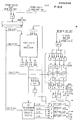
- the level 1 (Ll) directory in FIGURE 4 and the directory look-aside table (DLAT) in FIGURE 5 are conventional and are each constructed in the manner taught by the prior art.
- the processor (CPU) generates a storage request at Ll using a virtual address (VA).
- VA virtual address
- the bit positions in the virtual address going to the directory and DLAT are defined in FIGURE 3.
- the bit positions given in parenthesis as addresses to the DLAT, directories and caches in the detailed figures in this specification refer to the bit positions in FIGURE 3, which can apply to either a virtual address, real address or absolute address.
- Each entry in the directory and DLAT holds bit positions of both the virtual address (VA) and the translated absolute address (AA).
- VA bits are needed to compare with the CPU requested address which is a virtual address.
- the absolute address of each page represented in the DLAT is the translation of the VA needed to address main storage when there is an Ll directory noncompare (i.e. line miss).
- the Ll directory holds the absolute address of its valid entries.
- I/O channels and other processors cross- interrogate the Ll directory using an absolute address. There are cases when a line is valid in the Ll cache but there is no valid DLAT entry for it.
- the Ll directory, DLAT and DAT logic need not change when a L2 cache is put into the storage hierarchy.
- the major difference is that on a line miss (Ll directory non-compare) the absolute address from the DLAT is sent to L2 instead of to main storage (MS). If there is an L2 directory compare, the line is moved from the L2 cache to the Ll cache. If the L2 directory does not compare, then the absolute address is sent to MS, and the page is copied from MS into the L2 cache, the absolute address is stored in the L2 directory, and the requested line in the page is simultaneously copied into the Ll cache, and the requested double word(s) is simultaneously copied into the CPU.
- FIGURES 6 and 7 show a four-way set associative L2 cache and its L2 directory which are constructed in the prior- art manner of the Ll directory and Ll cache except for the novel R flag bit added for each L2 directory entry.
- Each L2 directory entry also holds an absolute address (AA) and other flag bits for a page of data in the L2 cache.
- the L2 circuits are made of slower but cheaper technology than the Ll circuits. However, the L2 circuits are faster than the MS circuit technology.
- the designation "page” is used to refer to each block in the L2 cache to differentiate an L2 block from the blocks in the Ll cache which are referred to as "lines".
- the L2 block size is equal to the page size managed by software in main storage which is usually referred to as a "page”.
- the Ll block size (line) is 64 or 128 bytes and the software managed page size is 4K bytes.
- a Ll line size of 128 bytes is used, and a L2 page size of 4096 bytes is used.
- the Ll directory, the L2 directory and the DLAT are each assumed to be four-way set associative, i.e. four entries in each congruence class.
- the DLAT may hold as many addresses as the L2 directory.
- the L2 cache preferably holds many more addresses than each processor's DLAT.
- the DLAT and the Ll and L2 caches shown in detail in FIGURES 4, 5, 6 and 7 each internally operate in the conventional manner, except for the L2 replacement selection function.
- the symbol C in a box is a concatenation function, in which each box concatenates the DLAT absolute address bits 1-19 with VA address bits 20-24 (which are the same as AA bits 20-24). They provide the selected entries AA on the DLAT absolute address output A, B, C or D.
- the processor initiates a MS request at level 1 by sending a virtual address to the DLAT and Ll directory, which select a congruence class in each.
- the DLAT array and Ll directory array each read out the four addresses of the selected class of entries A, B, C and D in parallel, which are compared with the virtual address from the processor.
- the dynamic address translation (DAT) circuit is requested to translate the virtual address to a real address by fetching an entry from each of the segment and page tables. This translated address is prefixed into an absolute address, which is then stored in the DLAT array, replacing the least-recently-used (LRU) entry in the DLAT when necessary.
- DAT dynamic address translation
- the requested VA compares with both the VA in the DLAT and in the Ll directory (line hit), then the associated word is read/stored from/in- to the Ll cache and the CPU request is complete. Over 95% of the CPU requests generally are accessed in this manner.
- the absolute address is obtained from the DLAT, which is selected by the requested address comparing with one of the four entry addresses (A, B, C or D) in the selected class.
- the absolute address from the selected DLAT entry is a page address which is concatenated with VA bits 20-24 to obtain a line address which is sent to the L2 cache directory for fetching the line from the L2 cache to the Ll cache, if the addressed page is in the L2 cache.
- the address of this fetched line is stored in the Ll directory.
- the Ll and L2 directories each use a different set of bit positions from the virtual and absolute addresses, respectively, to address the correct classes in the respective directories, because their block sizes are different.
- each entry in the L2 directory is provided with a "replacement flag" which is referred to as the "R" bit.
- the purpose of the R bit is to improve system performance by minimizing the cache misses at L2 for a given L2 cache capacity.
- FIGURE 8 illustrates the R flag bit in each entry in each L2 congruence class.
- FIGURE 7 illustrates the layout of a four-way associative L2 directory containing the congruence classes of FIGURE 8 as rows therein.
- the R flag enables CPU accesses to the DLAT at Ll to control the L2 page replacement selection.
- the DLAT page address replacement selection is the summation of the page access activity by the CPU, provided that the DLAT replacement selection is based on a LRU operation. That is, this invention inputs to the L2 page replacement selection function the Ll DLAT page replacement operation.
- the Ll DLAT replacement selection circuits may use the technique described in the IBM TDB article published July 1971 on page 430 by A. Weinberger entitled "Buffer Store Replacement by Selection Based on Probable Least Recent Usage".
- 1% or less of the CPU requests have a DLAT miss, which this invention provides as an input to the L2 cache replacement selection function.
- the 1% misses have a frequency rate much slower than the CPU request rate.
- the slower DLAT miss rate is capable of matching the slower switching speed of the L2 circuits, wherein the 99% DLAT hit rate would be a missmatch.
- Each DLAT miss normally replaces an existing DLAT entry to make room for the requesting VA and its translated page AA.
- the invention communicates each DLAT replaced page address to L2 to make the corresponding page a candidate for L2 cache replacement.
- the DLAT hits by CPU requested pages are only communicated to L2 if they have a Ll cache directory miss which occurs for about 5% of CPU requests.
- the Ll hits sample about 5% of the DLAT hits to reduce the DLAT hit frequency rate communicated to L2 to match the L2 circuit slow speed limitations.
- a summarization of the Ll DLAT hit occurrences is inherently included in the Ll DLAT page replacement determinations, i.e. a page is replaced because it did not have a sufficiently recent DLAT hit by any CPU request. Therefore, the low frequency DLAT replacement communication to L2 inherently represents the frequency of DLAT hits to L2, in the absence of the communication of DLAT hits.
- the L2 communicated DLAT misses enable correctional advantages for improving the replacement selection determinations for the DLAT.
- the DLAT hits after sampling by Ll cache hits and the DLAT misses have a combined low rate that can easily match the L2 circuit speed.
- the L2 cache replacement selection is not completely slaved to the DLAT page replacement decisions, and in many situations the L2 replacement function can refuse a DLAT replacement decision if subsequent CPU requests prove it was wrong, which can occasionally happen with any LRU determination. Or, in multi-processing, another CPU may still be accessing one or more lines in the page.
- the invention operates in an environment in which most CPU requests use virtual addresses.
- Statistical studies of the job streams on large IBM CPUs have found that 95% or more of the CPU requests use virtual addresses (i.e. DAT on). Therefore, the small percentage of CPU accesses using real addresses (i.e. DAT off) are expected to have an insignificant effect on the L2 replacement selection operations controlled by this invention.
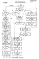
- FIGURE 2 is a flow diagram of the method of this invention. If DAT is on (i.e. CPU requests use VAs), some CPU requests will miss in the DLAT and displace other entries in the DLAT. The displaced page address is sent to L2 to select the corresponding L2 directory entry. Box 21 turns on the R flag in the L2 entry selected by the DLAT replaced page address, to make this L2 entry a candidate for L2 replacement.
- the DLAT miss is one of two DLAT events used by this invention to communicate an R setting from Ll to L2.
- This invention takes advantage of the fact that a Ll to L2 communication occurs for a Ll miss, regardless of the existence of this invention in the storage hierarchy. That is, this invention uses the existing Ll hit communication to filter the communication of DLAT hits from the large number of DLAT hits occurring at high frequency. Hence, very little additional hardware is needed to communicate the filtered DLAT hits. In other words, the particular type of DLAT hit filtering obtained by the Ll cache miss permits the use of Ll to L2 communication hardware provided for normal line fetch requests to L2.
- the DLAT miss communications by this invention do not necessarily overlap Ll cache misses, but DLAT misses also occur at a low frequency, (i.e. for less than 1% of CPU requests).
- the R flag control method in FIGURE 2 handles intermixed CPU real addresse (RA) requests. If requested RAs are put into the DLAT, the invention will operate in the same manner with RAs as with VAs. However, most large CPUs only used the DLAT for VAs and RAs bypass the DLAT but access the Ll cache. The preferred method embodiment in FIGURE 2 assumes the latter.
- Each RA request having a Ll cache miss has its requested address sent to L2 to select its L2 page entry and turn off that page's R flag in box 26. Also, an Ll cache miss usually causes a replaced address in the Ll cache congruence class addressed by the missed RA request.
- This Ll cache replaced address is also sent to L2 to select its L2 page entry and turn on its R flag in box 27 to make this L2 entry a candidate for L2 replacement.
- RA Ll misses occur at a low frequency (i.e. for less than 5% of CPU requests).
- the frequency rate for the communications from Ll to L2 for the R bit operations is 1/20 to 1/10 of the L1 operation rate for CPU requests.
- the preferred embodiment's slower rate of communicated R bit switching signals can be handled easily by the L2 cache directory circuits which are usually made of slower, cheaper circuits than the Ll directory, Ll cache, or DLAT.
- the Ll to L2 communication of the R bit switching signals were done for hit as well as miss signals (i.e. at the Ll rate)
- a slower L2 technology could not handle the Ll rate.
- DLAT hits which have cache hits take path 29 in FIGURE 2 and are not communicated to L2 in the preferred embodiment because their rate of occurrence is too fast for the assumed L2 circuit speed limitation.
- the inventive concept in this application also includes the communication of all DLAT hits to L2 so that each DLAT hit could turn off the R bit for the DLAT requested page entries in the L2 cache.
- the non-communication to L2 of the DLAT hit having a Ll hit to turn off the R flag in the preferred embodiment is a tradeoff which would require L2 to have a very fast R bit switching circuits that could operate at Ll speeds, which may increase cost without significantly improving the L2 replacement efficiency.
- Multi-processing with a common L2 cache would require even faster switching circuits than at Ll of each processor. In the latter case, the R bit handling circuits could be made of faster technology to handle the Ll rate while the remainder of L2 is made of the slower, cheaper technology.
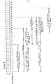
- TABLE 1 represents the conditions in the preferred embodiment for the communication (and non-communication) of R flag switching signals from Ll to L2 for virtual address CPU requests, as follows:
- the six rows indicate the different combi- .nations for the states of the DLAT, Ll directory, and L2 directory, and the resulting communication from Ll (if any) to switch the R flag bits, and whether the selected R flag is associated with the CPU requested page address or the DLAT replaced address.
- the DLAT circuits shown in FIGURE 5 and the replacement array and replacement selection circuits for the DLAT shown in FIGURE 9 are considered conventional with the DLAT replacement operating in the conventional manner according to the article previously cited herein as published in the IBM Technical Disclosure Bulletin in July 1971 by A. Weinberger.
- These DLAT circuits and the conventional Ll cache circuits shown in FIGURE 4 are illustrated for the purpose of showing that they are part of the inventive combination of circuits embodying this invention shown in FIGURE 1.
- the required L2 entry is selected in the L2 directory in FIGURES 6 and 7 by the absolute address on the DLAT address out bus shown in FIGURE 10, which selects the DLAT replaced address on a DLAT miss, or the CPU requested address on a DLAT hit.
- No R bit operation occurs when the DLAT and Ll cache both have hits in the preferred embodiment, which therefore does not provide an output from FIGURE 10.
- the R turn off circuits in FIGURE 11 input either (1) the active one of the four L2 compare (CPR) lines that identifies a L2 entry selected by the current CPU request, or (2) the active one of the four L2 replace lines that identifies a L2 cache replacement entry containing the address of the Ll referenced page when none of the four L2 compare lines provides an active signal.
- CPR L2 compare
- FIGURE 12 shows the R bit turn on circuits which are activated by either: (1) a DLAT miss signal from FIGURE 5, or (2) a CPU real address request with DAT off.
- the L2 compare signals are provided only when either there is (1) a DLAT replacement address on the DLAT address out bus from FIGURE 10 when DAT is on, or (2) an Ll replacement address out bus signal from FIGURE 17 when DAT is off.
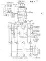
- FIGURE 13 represents the L2 replacement candidate selection circuits and is inclusive of the circuits in FIGURES 14, 15 and 16.
- the L2 LRU address register 41 receives either the DLAT requested or replacement address from FIGURE 10, the Ll directory address from FIGURE 4, or the Ll replacement address from FIGURE 17. This address in register 41 selects a row of three bits in the L2 LRU array 42 (which may be constructed in the same manner as the Ll LRU array or DLAT LRU array).
- the LRU array per se, operates in the manner of prior art LRU arrays found for example in prior IBM machines, and described in the previously cited Weinberger article published in 1971.
- An example of an Ll LRU array is disclosed in European Patent application 82100836.4 filed February 5, 1982, and entitled "Store-in-Cache Multiprocessor System with checkpoint feature".
- Each of the rows in the L2 and each other LRU array in this embodiment corresponds to a respective row in the respective cache (i.e. congruence class) having four entries, i.e. A, B, C and D.
- the setting of the three bits (AB), (A) and (D) in the selected LRU array row point to one of the four entries A, B, C, D in the respective cache or DLAT which is currently the most available candidate for being replaced in the selected congruence class. Only one LRU candidate in each class is pointed to by the LRU array. A valid replacement candidate remains useable until it is actually replaced. Any invalid entry in the class will be replaced before any valid entry that is indicated by the LRU pointer for the same congruence class.
- the settings of the LRU bits (AB), (A), (D) in the replacement array 42 in FIGURE 15 are determined by the accesses to the slots A, B, C and D in each congruence class, according to the following TABLE 2:
- TABLE 2 and TABLE 3 are old in the art, having been disclosed in the previously cited July 1971, IBM Technical Disclosure Bulletin article by Arnold Weiriberger.
- the selected row in array 42 is outputted into a replacement array register 43 in which the three row bits (AB), (A) and (D) may be updated by the circuits in FIGURE 15 when the novel control provided by the circuits in FIGURE 14 generate an update signal.
- the readout row in register 43 is not changed.
- FIGURE 16 represents conventional prior art circuits which receive the current content of the replacement array output register to select a replacement candidate from among the four entries in a currently selected class in the L2 cache.
- This invention pertains to a novel method and means for setting the L2 replacement array to control the selection of the LRU candidate entry in each class in the L2 directory.
- the novel circuits in FIGURE 14 provide an update L2 LRU array signal whenever any R bit changes state, i.e. from off to on, or from on to off.
- the circuits in FIGURE 14 do not provide any update signal whenever a turned on R bit again receives a turn on signal, which is a characteristic important to this invention in this embodiment, which will become apparent later.
- An update signal is provided whenever a turned off R bit again receives a turn off signal.
- a L2 compare signal is provided to FIGURE 14 and FIGURE 15 from the L2 cache whenever the Ll address being provided from FIGURE 10 on the DLAT address bus out compares-equal with the address contained in one of the entries in the selected class in the L2 directory to indicate that this L2 entry represents an L2 page being either hit or replaced by the DLAT, or by a real address made in the Ll cache, thereby causing the R flag for that L2 entry to be set either off or on.
- the circuits in FIGURE 15 use the update L2 LRU array signal to generate a three bit pointer for the L2 LRU array congruence class currently being selected in the L2 cache.
- the pointer selects a replacement candidate among the entries A, B, C, or D in the selected class.
- the circuits in FIGURE 15 are controlled in a very subtle manner by the update signal from FIGURE 14 to cause the LRU array settings to operate in accordance with this invention. It is noted that the occurrence of the update signals to FIGURE 15 is selective of which R bit switching signal is allowed to generate an update signal.
- the active one of the L2A, L2B, L2C, or L2D compare (CPR) inputs identifies which of the four entries is having its R flag state tested, i.e. either A, B, C or D, so that if the selected R flag is on, then no second turn on signal is permitted to generate an update signal to FIGURE 15.
- the effect of the operation by the circuits in FIGURES 14 and 15 is to set the current L2 class pointer (i.e. addressed row in the LRU array) to point away from any L2 entry having its R flag switched on or off (i.e. to point to a different L2 entry in the class than the selected entry). This prevents any entry having its R flag switched from being immediately made the LRU replacement candidate, and it cannot then be immediately replaced. Thus, an entry having its R flag switched on is not immediately made the LRU replacement candidate, and it cannot then be immediately replaced. However, any R flag which is in an on state will not again generate an update L2 LRU array signal until that R flag is set off.
- the single turn-on characteristic of the circuit in FIGURE 15 is particularly important in a multi-processor system to prevent a second CPU from causing a second turn on signal to the LRU array for a R flag previously turned on by another CPU, because a second turn on signal to the LRU array would change the LRU status of the entry by having it age from the most recently turned on, rather than from its first turn on which should control its LRU status as a replacement candidate.
- Any multiprogrammed system whether in a uiiiprocessor or a multiprocessor, often causes a particular job to execute, get task switched out of the CPU, and shortly thereafter get task switched back into the CPU, etc.
- Task switching a job into and out of a CPU a number of times is a common situation.
- lines of data get moved into the CPU Ll cache and the active page addresses are translated into the CPU DLAT.
- these lines and page addresses quickly get replaced in the CPU's Ll cache and DLAT.
- L2 may be a liability to the system by actually increasing the time loss for the Ll cache to get its requested lines after subsequent task switches.
- This task example analysis shows why the page replacement operation in L2 should respond at a much slower rate than the page address replacements in the DLAT or the line replacements in the Ll cache, in order to avoid ping-ponging pages between L2 and L3to maximize the performance of the system.
- L2 must have a longer page replacement "time constant" than the DLAT to enable L2 to increase system performance.
- the LRU pointer generated for that class will point away from the currently addressed entry, but may have the beneficial result of pointing at the other entry having the older turned on R flag, which then becomes the replacement candidate.
- the effect of the R flag switch offs in FIGURE 15 is to cause communicated DLAT hits to reset the LRU aging of the selected entry, which tends to prevent its selection as a replacement candidate.
- DLAT hits.having Ll cache misses are immediately reflected into the L2 replacement candidacy of the L2 page entry having the CPU request.
- DLAT misses which turn on an R flag will operate the same as before.
- the LRU pointer selects the entry having the R flag on for the longest time.
- the LRU pointer still selects the LRU entry among the entries in the class, regardless of the off state of the R flags since the static states of the R flags are ignored by the LRU replacement selection circuits when generating an LRU pointer.
Landscapes
- Engineering & Computer Science (AREA)
- Theoretical Computer Science (AREA)
- Physics & Mathematics (AREA)
- General Engineering & Computer Science (AREA)
- General Physics & Mathematics (AREA)
- Memory System Of A Hierarchy Structure (AREA)
Applications Claiming Priority (2)
| Application Number | Priority Date | Filing Date | Title |
|---|---|---|---|
| US06/280,759 US4464712A (en) | 1981-07-06 | 1981-07-06 | Second level cache replacement method and apparatus |
| US280759 | 1988-12-06 |
Publications (3)
| Publication Number | Publication Date |
|---|---|
| EP0069250A2 true EP0069250A2 (fr) | 1983-01-12 |
| EP0069250A3 EP0069250A3 (en) | 1985-08-07 |
| EP0069250B1 EP0069250B1 (fr) | 1988-06-01 |
Family
ID=23074508
Family Applications (1)
| Application Number | Title | Priority Date | Filing Date |
|---|---|---|---|
| EP82105208A Expired EP0069250B1 (fr) | 1981-07-06 | 1982-06-15 | Commande de remplacement de données dans un cache de second niveau |
Country Status (4)
| Country | Link |
|---|---|
| US (1) | US4464712A (fr) |
| EP (1) | EP0069250B1 (fr) |
| JP (1) | JPS6043540B2 (fr) |
| DE (1) | DE3278587D1 (fr) |
Cited By (6)
| Publication number | Priority date | Publication date | Assignee | Title |
|---|---|---|---|---|
| EP0170525A3 (fr) * | 1984-07-31 | 1989-09-13 | Texas Instruments Incorporated | Projet de hiérarchie d'antémémoires à utiliser dans une unité de gestion de mémoire |
| EP0243724A3 (fr) * | 1986-05-01 | 1990-05-23 | International Business Machines Corporation | Hiérarchie de mémoires à niveaux multiples avec mode d'adressage variable |
| US4985829A (en) * | 1984-07-31 | 1991-01-15 | Texas Instruments Incorporated | Cache hierarchy design for use in a memory management unit |
| EP0461923A3 (en) * | 1990-06-15 | 1992-03-25 | Compaq Computer Corporation | True least recently used replacement method and apparatus |
| EP0490525A3 (en) * | 1990-12-14 | 1993-10-27 | Ibm | Removal of data from a shared cache |
| WO2017172328A1 (fr) * | 2016-03-31 | 2017-10-05 | Qualcomm Incorporated | Mécanisme de préanalyse pour la réparation d'un défaut de demande |
Families Citing this family (77)
| Publication number | Priority date | Publication date | Assignee | Title |
|---|---|---|---|---|
| JPS5687282A (en) * | 1979-12-14 | 1981-07-15 | Nec Corp | Data processor |
| JPS58147879A (ja) * | 1982-02-26 | 1983-09-02 | Toshiba Corp | キヤツシユメモリ制御方式 |
| JPS5994289A (ja) * | 1982-11-22 | 1984-05-30 | Hitachi Ltd | 記憶制御方式 |
| US4731739A (en) * | 1983-08-29 | 1988-03-15 | Amdahl Corporation | Eviction control apparatus |
| JPH065541B2 (ja) * | 1983-12-30 | 1994-01-19 | 株式会社日立製作所 | 論理回路の自動設計方法 |
| US4747043A (en) * | 1984-02-10 | 1988-05-24 | Prime Computer, Inc. | Multiprocessor cache coherence system |
| US4747044A (en) * | 1984-08-23 | 1988-05-24 | Ncr Corporation | Direct execution of software on microprogrammable hardware |
| US4648033A (en) * | 1984-09-07 | 1987-03-03 | International Business Machines Corporation | Look-aside buffer LRU marker controller |
| US4991081A (en) * | 1984-10-31 | 1991-02-05 | Texas Instruments Incorporated | Cache memory addressable by both physical and virtual addresses |
| US4774654A (en) * | 1984-12-24 | 1988-09-27 | International Business Machines Corporation | Apparatus and method for prefetching subblocks from a low speed memory to a high speed memory of a memory hierarchy depending upon state of replacing bit in the low speed memory |
| US4860192A (en) * | 1985-02-22 | 1989-08-22 | Intergraph Corporation | Quadword boundary cache system |
| US4899275A (en) * | 1985-02-22 | 1990-02-06 | Intergraph Corporation | Cache-MMU system |
| US5255384A (en) * | 1985-02-22 | 1993-10-19 | Intergraph Corporation | Memory address translation system having modifiable and non-modifiable translation mechanisms |
| US4884197A (en) * | 1985-02-22 | 1989-11-28 | Intergraph Corporation | Method and apparatus for addressing a cache memory |
| US4933835A (en) * | 1985-02-22 | 1990-06-12 | Intergraph Corporation | Apparatus for maintaining consistency of a cache memory with a primary memory |
| US4737909A (en) * | 1985-04-01 | 1988-04-12 | National Semiconductor Corp. | Cache memory address apparatus |
| US4755930A (en) * | 1985-06-27 | 1988-07-05 | Encore Computer Corporation | Hierarchical cache memory system and method |
| US5029072A (en) * | 1985-12-23 | 1991-07-02 | Motorola, Inc. | Lock warning mechanism for a cache |
| US5237671A (en) * | 1986-05-02 | 1993-08-17 | Silicon Graphics, Inc. | Translation lookaside buffer shutdown scheme |
| US4757447A (en) * | 1986-07-28 | 1988-07-12 | Amdahl Corporation | Virtual memory system having identity marking for common address space |
| US4814981A (en) * | 1986-09-18 | 1989-03-21 | Digital Equipment Corporation | Cache invalidate protocol for digital data processing system |
| US5091846A (en) * | 1986-10-03 | 1992-02-25 | Intergraph Corporation | Cache providing caching/non-caching write-through and copyback modes for virtual addresses and including bus snooping to maintain coherency |
| US5095424A (en) * | 1986-10-17 | 1992-03-10 | Amdahl Corporation | Computer system architecture implementing split instruction and operand cache line-pair-state management |
| US4926317A (en) * | 1987-07-24 | 1990-05-15 | Convex Computer Corporation | Hierarchical memory system with logical cache, physical cache, and address translation unit for generating a sequence of physical addresses |
| JP2965987B2 (ja) * | 1988-02-22 | 1999-10-18 | 株式会社日立製作所 | データ処理システム |
| US5097409A (en) * | 1988-06-30 | 1992-03-17 | Wang Laboratories, Inc. | Multi-processor system with cache memories |
| US4939641A (en) * | 1988-06-30 | 1990-07-03 | Wang Laboratories, Inc. | Multi-processor system with cache memories |
| JPH0228738A (ja) * | 1988-07-18 | 1990-01-30 | Nippon Telegr & Teleph Corp <Ntt> | 多階層キャッシュメモリのブロック置換え方法 |
| US5317716A (en) * | 1988-08-16 | 1994-05-31 | International Business Machines Corporation | Multiple caches using state information indicating if cache line was previously modified and type of access rights granted to assign access rights to cache line |
| US6092153A (en) * | 1988-11-14 | 2000-07-18 | Lass; Stanley Edwin | Subsettable top level cache |
| US5159677A (en) * | 1988-11-21 | 1992-10-27 | International Business Machines Corp. | Method and system for storing data in and retrieving data from a non-main storage virtual data space |
| US5202972A (en) * | 1988-12-29 | 1993-04-13 | International Business Machines Corporation | Store buffer apparatus in a multiprocessor system |
| US6038641A (en) * | 1988-12-30 | 2000-03-14 | Packard Bell Nec | Two stage cache memory system and method |
| US5060136A (en) * | 1989-01-06 | 1991-10-22 | International Business Machines Corp. | Four-way associative cache with dlat and separately addressable arrays used for updating certain bits without reading them out first |
| US5287484A (en) * | 1989-06-21 | 1994-02-15 | Hitachi, Ltd. | Multi-processor system for invalidating hierarchical cache |
| US5150472A (en) * | 1989-10-20 | 1992-09-22 | International Business Machines Corp. | Cache management method and apparatus for shared, sequentially-accessed, data |
| JP2833062B2 (ja) * | 1989-10-30 | 1998-12-09 | 株式会社日立製作所 | キャッシュメモリ制御方法とこのキャッシュメモリ制御方法を用いたプロセッサおよび情報処理装置 |
| US5307477A (en) * | 1989-12-01 | 1994-04-26 | Mips Computer Systems, Inc. | Two-level cache memory system |
| US5136700A (en) * | 1989-12-22 | 1992-08-04 | Digital Equipment Corporation | Apparatus and method for reducing interference in two-level cache memories |
| US5261066A (en) * | 1990-03-27 | 1993-11-09 | Digital Equipment Corporation | Data processing system and method with small fully-associative cache and prefetch buffers |
| US5197139A (en) * | 1990-04-05 | 1993-03-23 | International Business Machines Corporation | Cache management for multi-processor systems utilizing bulk cross-invalidate |
| US5014195A (en) * | 1990-05-10 | 1991-05-07 | Digital Equipment Corporation, Inc. | Configurable set associative cache with decoded data element enable lines |
| JPH0443876A (ja) * | 1990-06-08 | 1992-02-13 | Hanix Ind Co Ltd | 建設機械の油圧装置における出力制御装置 |
| ATE170642T1 (de) * | 1990-06-15 | 1998-09-15 | Compaq Computer Corp | Mehrstufeneinschluss in mehrstufigen cache- speicherhierarchien |
| US5283876A (en) * | 1990-10-05 | 1994-02-01 | Bull Hn Information Systems Inc. | Virtual memory unit utilizing set associative memory structure and state machine control sequencing with selective retry |
| US5412787A (en) * | 1990-11-21 | 1995-05-02 | Hewlett-Packard Company | Two-level TLB having the second level TLB implemented in cache tag RAMs |
| US5249282A (en) * | 1990-11-21 | 1993-09-28 | Benchmarq Microelectronics, Inc. | Integrated cache memory system with primary and secondary cache memories |
| US5530823A (en) * | 1992-05-12 | 1996-06-25 | Unisys Corporation | Hit enhancement circuit for page-table-look-aside-buffer |
| JP3049158B2 (ja) * | 1992-09-24 | 2000-06-05 | キヤノン株式会社 | 文字処理装置および文字処理装置の文字処理方法 |
| JPH06282488A (ja) * | 1993-03-25 | 1994-10-07 | Mitsubishi Electric Corp | キャッシュ記憶装置 |
| US5689679A (en) * | 1993-04-28 | 1997-11-18 | Digital Equipment Corporation | Memory system and method for selective multi-level caching using a cache level code |
| US5539893A (en) * | 1993-11-16 | 1996-07-23 | Unisys Corporation | Multi-level memory and methods for allocating data most likely to be used to the fastest memory level |
| US5845310A (en) * | 1993-12-15 | 1998-12-01 | Hewlett-Packard Co. | System and methods for performing cache latency diagnostics in scalable parallel processing architectures including calculating CPU idle time and counting number of cache misses |
| US5604753A (en) * | 1994-01-04 | 1997-02-18 | Intel Corporation | Method and apparatus for performing error correction on data from an external memory |
| US5870599A (en) * | 1994-03-01 | 1999-02-09 | Intel Corporation | Computer system employing streaming buffer for instruction preetching |
| US5577227A (en) * | 1994-08-04 | 1996-11-19 | Finnell; James S. | Method for decreasing penalty resulting from a cache miss in multi-level cache system |
| US5606688A (en) * | 1994-08-31 | 1997-02-25 | International Business Machines Corporation | Method and apparatus for dynamic cache memory allocation via single-reference residency times |
| US5584013A (en) * | 1994-12-09 | 1996-12-10 | International Business Machines Corporation | Hierarchical cache arrangement wherein the replacement of an LRU entry in a second level cache is prevented when the cache entry is the only inclusive entry in the first level cache |
| US6047357A (en) * | 1995-01-27 | 2000-04-04 | Digital Equipment Corporation | High speed method for maintaining cache coherency in a multi-level, set associative cache hierarchy |
| US5894564A (en) * | 1995-06-07 | 1999-04-13 | International Business Machines Corporation | System for identifying memory segment bounded by previously accessed memory locations within data block and transferring thereof only when the segment has been changed |
| US5897651A (en) * | 1995-11-13 | 1999-04-27 | International Business Machines Corporation | Information handling system including a direct access set associative cache and method for accessing same |
| US5787486A (en) * | 1995-12-15 | 1998-07-28 | International Business Machines Corporation | Bus protocol for locked cycle cache hit |
| US5778422A (en) * | 1996-04-04 | 1998-07-07 | International Business Machines Corporation | Data processing system memory controller that selectively caches data associated with write requests |
| US6138209A (en) * | 1997-09-05 | 2000-10-24 | International Business Machines Corporation | Data processing system and multi-way set associative cache utilizing class predict data structure and method thereof |
| US6138208A (en) * | 1998-04-13 | 2000-10-24 | International Business Machines Corporation | Multiple level cache memory with overlapped L1 and L2 memory access |
| US6732238B1 (en) * | 2001-06-08 | 2004-05-04 | Tensilica, Inc. | Set-associative cache memory having variable time decay rewriting algorithm |
| US6996676B2 (en) * | 2002-11-14 | 2006-02-07 | International Business Machines Corporation | System and method for implementing an adaptive replacement cache policy |
| US7284095B2 (en) * | 2004-08-18 | 2007-10-16 | International Business Machines Corporation | Latency-aware replacement system and method for cache memories |
| US20060179231A1 (en) * | 2005-02-07 | 2006-08-10 | Advanced Micron Devices, Inc. | System having cache memory and method of accessing |
| US7930484B2 (en) * | 2005-02-07 | 2011-04-19 | Advanced Micro Devices, Inc. | System for restricted cache access during data transfers and method thereof |
| US8606998B2 (en) * | 2006-08-24 | 2013-12-10 | Advanced Micro Devices, Inc. | System and method for instruction-based cache allocation policies |
| US20080313407A1 (en) * | 2007-06-13 | 2008-12-18 | Zhigang Hu | Latency-aware replacement system and method for cache memories |
| US8171223B2 (en) * | 2008-12-03 | 2012-05-01 | Intel Corporation | Method and system to increase concurrency and control replication in a multi-core cache hierarchy |
| GB2506900A (en) * | 2012-10-12 | 2014-04-16 | Ibm | Jump positions in recording lists during prefetching |
| US9274971B2 (en) * | 2012-11-27 | 2016-03-01 | International Business Machines Corporation | Low latency data exchange |
| US10558571B2 (en) | 2014-03-20 | 2020-02-11 | Sybase, Inc. | Second level database file cache for row instantiation |
| CN112579482B (zh) * | 2020-12-05 | 2022-10-21 | 西安翔腾微电子科技有限公司 | 一种非阻塞Cache替换信息表超前精确更新装置及方法 |
Family Cites Families (15)
| Publication number | Priority date | Publication date | Assignee | Title |
|---|---|---|---|---|
| US3723976A (en) * | 1972-01-20 | 1973-03-27 | Ibm | Memory system with logical and real addressing |
| US3806883A (en) * | 1972-11-22 | 1974-04-23 | Rca Corp | Least recently used location indicator |
| US3866183A (en) * | 1973-08-31 | 1975-02-11 | Honeywell Inf Systems | Communications control apparatus for the use with a cache store |
| US3845474A (en) * | 1973-11-05 | 1974-10-29 | Honeywell Inf Systems | Cache store clearing operation for multiprocessor mode |
| US3949368A (en) * | 1974-01-23 | 1976-04-06 | Data General Corporation | Automatic data priority technique |
| US3949369A (en) * | 1974-01-23 | 1976-04-06 | Data General Corporation | Memory access technique |
| US3938097A (en) * | 1974-04-01 | 1976-02-10 | Xerox Corporation | Memory and buffer arrangement for digital computers |
| US4077059A (en) * | 1975-12-18 | 1978-02-28 | Cordi Vincent A | Multi-processing system with a hierarchial memory having journaling and copyback |
| US4070706A (en) * | 1976-09-20 | 1978-01-24 | Sperry Rand Corporation | Parallel requestor priority determination and requestor address matching in a cache memory system |
| US4181937A (en) * | 1976-11-10 | 1980-01-01 | Fujitsu Limited | Data processing system having an intermediate buffer memory |
| US4195343A (en) * | 1977-12-22 | 1980-03-25 | Honeywell Information Systems Inc. | Round robin replacement for a cache store |
| JPS5849945B2 (ja) * | 1977-12-29 | 1983-11-08 | 富士通株式会社 | バツフア合せ方式 |
| US4168541A (en) * | 1978-09-25 | 1979-09-18 | Sperry Rand Corporation | Paired least recently used block replacement system |
| US4322795A (en) * | 1980-01-24 | 1982-03-30 | Honeywell Information Systems Inc. | Cache memory utilizing selective clearing and least recently used updating |
| US4332010A (en) * | 1980-03-17 | 1982-05-25 | International Business Machines Corporation | Cache synonym detection and handling mechanism |
-
1981
- 1981-07-06 US US06/280,759 patent/US4464712A/en not_active Expired - Lifetime
-
1982
- 1982-06-15 EP EP82105208A patent/EP0069250B1/fr not_active Expired
- 1982-06-15 DE DE8282105208T patent/DE3278587D1/de not_active Expired
- 1982-07-01 JP JP57112616A patent/JPS6043540B2/ja not_active Expired
Cited By (8)
| Publication number | Priority date | Publication date | Assignee | Title |
|---|---|---|---|---|
| EP0170525A3 (fr) * | 1984-07-31 | 1989-09-13 | Texas Instruments Incorporated | Projet de hiérarchie d'antémémoires à utiliser dans une unité de gestion de mémoire |
| US4985829A (en) * | 1984-07-31 | 1991-01-15 | Texas Instruments Incorporated | Cache hierarchy design for use in a memory management unit |
| EP0243724A3 (fr) * | 1986-05-01 | 1990-05-23 | International Business Machines Corporation | Hiérarchie de mémoires à niveaux multiples avec mode d'adressage variable |
| EP0461923A3 (en) * | 1990-06-15 | 1992-03-25 | Compaq Computer Corporation | True least recently used replacement method and apparatus |
| US5325511A (en) * | 1990-06-15 | 1994-06-28 | Compaq Computer Corp. | True least recently used replacement method and apparatus |
| EP0490525A3 (en) * | 1990-12-14 | 1993-10-27 | Ibm | Removal of data from a shared cache |
| WO2017172328A1 (fr) * | 2016-03-31 | 2017-10-05 | Qualcomm Incorporated | Mécanisme de préanalyse pour la réparation d'un défaut de demande |
| US9934149B2 (en) | 2016-03-31 | 2018-04-03 | Qualcomm Incorporated | Prefetch mechanism for servicing demand miss |
Also Published As
| Publication number | Publication date |
|---|---|
| JPS6043540B2 (ja) | 1985-09-28 |
| EP0069250B1 (fr) | 1988-06-01 |
| US4464712A (en) | 1984-08-07 |
| DE3278587D1 (en) | 1988-07-07 |
| JPS589277A (ja) | 1983-01-19 |
| EP0069250A3 (en) | 1985-08-07 |
Similar Documents
| Publication | Publication Date | Title |
|---|---|---|
| EP0069250B1 (fr) | Commande de remplacement de données dans un cache de second niveau | |
| US5123101A (en) | Multiple address space mapping technique for shared memory wherein a processor operates a fault handling routine upon a translator miss | |
| US5230045A (en) | Multiple address space system including address translator for receiving virtual addresses from bus and providing real addresses on the bus | |
| US5274790A (en) | Cache memory apparatus having a plurality of accessibility ports | |
| US5584013A (en) | Hierarchical cache arrangement wherein the replacement of an LRU entry in a second level cache is prevented when the cache entry is the only inclusive entry in the first level cache | |
| US6282617B1 (en) | Multiple variable cache replacement policy | |
| JP2557174B2 (ja) | データのセット位置の予測装置 | |
| US6622219B2 (en) | Shared write buffer for use by multiple processor units | |
| EP0062165B1 (fr) | Ordinateurs de multitraitement avec mémoires tampon particulières et en commun | |
| CA1059643A (fr) | Circuit de mise en fonction d'un algorithme a lru de remplacement dans une cache | |
| EP0071719B1 (fr) | Appareil de traitement de données comprenant un sous-système de mémoire à pagination | |
| US5751990A (en) | Abridged virtual address cache directory | |
| US4797814A (en) | Variable address mode cache | |
| US6047357A (en) | High speed method for maintaining cache coherency in a multi-level, set associative cache hierarchy | |
| US5590379A (en) | Method and apparatus for cache memory access with separate fetch and store queues | |
| US5553263A (en) | Cache memory system with fault tolerance having concurrently operational cache controllers processing disjoint groups of memory | |
| CA1212483A (fr) | Dispositif de selection de donnees par comparaison | |
| US20070094450A1 (en) | Multi-level cache architecture having a selective victim cache | |
| US6571316B1 (en) | Cache memory array for multiple address spaces | |
| US5829051A (en) | Apparatus and method for intelligent multiple-probe cache allocation | |
| EP0284751B1 (fr) | Mémoire cache | |
| KR920001282B1 (ko) | 버퍼메모리 제어장치 | |
| US5479629A (en) | Method and apparatus for translation request buffer and requestor table for minimizing the number of accesses to the same address | |
| EP0173893B1 (fr) | Système calculateur et méthode pour la préextraction de jeu de travail pour antémémoires de second niveau | |
| US6480940B1 (en) | Method of controlling cache memory in multiprocessor system and the multiprocessor system based on detection of predetermined software module |
Legal Events
| Date | Code | Title | Description |
|---|---|---|---|
| PUAI | Public reference made under article 153(3) epc to a published international application that has entered the european phase |
Free format text: ORIGINAL CODE: 0009012 |
|
| AK | Designated contracting states |
Designated state(s): DE FR GB |
|
| 17P | Request for examination filed |
Effective date: 19830519 |
|
| PUAL | Search report despatched |
Free format text: ORIGINAL CODE: 0009013 |
|
| AK | Designated contracting states |
Designated state(s): DE FR GB |
|
| 17Q | First examination report despatched |
Effective date: 19861112 |
|
| GRAA | (expected) grant |
Free format text: ORIGINAL CODE: 0009210 |
|
| AK | Designated contracting states |
Kind code of ref document: B1 Designated state(s): DE FR GB |
|
| REF | Corresponds to: |
Ref document number: 3278587 Country of ref document: DE Date of ref document: 19880707 |
|
| ET | Fr: translation filed | ||
| PLBE | No opposition filed within time limit |
Free format text: ORIGINAL CODE: 0009261 |
|
| STAA | Information on the status of an ep patent application or granted ep patent |
Free format text: STATUS: NO OPPOSITION FILED WITHIN TIME LIMIT |
|
| 26N | No opposition filed | ||
| PGFP | Annual fee paid to national office [announced via postgrant information from national office to epo] |
Ref country code: FR Payment date: 19960607 Year of fee payment: 15 |
|
| PGFP | Annual fee paid to national office [announced via postgrant information from national office to epo] |
Ref country code: DE Payment date: 19960628 Year of fee payment: 15 |
|
| PG25 | Lapsed in a contracting state [announced via postgrant information from national office to epo] |
Ref country code: FR Free format text: LAPSE BECAUSE OF NON-PAYMENT OF DUE FEES Effective date: 19980227 |
|
| PG25 | Lapsed in a contracting state [announced via postgrant information from national office to epo] |
Ref country code: DE Free format text: LAPSE BECAUSE OF NON-PAYMENT OF DUE FEES Effective date: 19980303 |
|
| REG | Reference to a national code |
Ref country code: FR Ref legal event code: ST |
|
| REG | Reference to a national code |
Ref country code: FR Ref legal event code: ST |
|
| PGFP | Annual fee paid to national office [announced via postgrant information from national office to epo] |
Ref country code: GB Payment date: 20010604 Year of fee payment: 20 |
|
| REG | Reference to a national code |
Ref country code: GB Ref legal event code: IF02 |
|
| PG25 | Lapsed in a contracting state [announced via postgrant information from national office to epo] |
Ref country code: GB Free format text: LAPSE BECAUSE OF EXPIRATION OF PROTECTION Effective date: 20020614 |
|
| REG | Reference to a national code |
Ref country code: GB Ref legal event code: PE20 Effective date: 20020614 |