EP0069853A2 - TTL logisches Tor - Google Patents
TTL logisches Tor Download PDFInfo
- Publication number
- EP0069853A2 EP0069853A2 EP82104710A EP82104710A EP0069853A2 EP 0069853 A2 EP0069853 A2 EP 0069853A2 EP 82104710 A EP82104710 A EP 82104710A EP 82104710 A EP82104710 A EP 82104710A EP 0069853 A2 EP0069853 A2 EP 0069853A2
- Authority
- EP
- European Patent Office
- Prior art keywords
- transistor
- base
- terminal
- output
- collector
- Prior art date
- Legal status (The legal status is an assumption and is not a legal conclusion. Google has not performed a legal analysis and makes no representation as to the accuracy of the status listed.)
- Granted
Links
Images
Classifications
-
- H—ELECTRICITY
- H03—ELECTRONIC CIRCUITRY
- H03K—PULSE TECHNIQUE
- H03K19/00—Logic circuits, i.e. having at least two inputs acting on one output; Inverting circuits
- H03K19/02—Logic circuits, i.e. having at least two inputs acting on one output; Inverting circuits using specified components
- H03K19/08—Logic circuits, i.e. having at least two inputs acting on one output; Inverting circuits using specified components using semiconductor devices
- H03K19/082—Logic circuits, i.e. having at least two inputs acting on one output; Inverting circuits using specified components using semiconductor devices using bipolar transistors
- H03K19/088—Transistor-transistor logic
-
- H—ELECTRICITY
- H03—ELECTRONIC CIRCUITRY
- H03K—PULSE TECHNIQUE
- H03K19/00—Logic circuits, i.e. having at least two inputs acting on one output; Inverting circuits
- H03K19/0008—Arrangements for reducing power consumption
- H03K19/001—Arrangements for reducing power consumption in bipolar transistor circuits
-
- H—ELECTRICITY
- H03—ELECTRONIC CIRCUITRY
- H03K—PULSE TECHNIQUE
- H03K19/00—Logic circuits, i.e. having at least two inputs acting on one output; Inverting circuits
- H03K19/01—Modifications for accelerating switching
- H03K19/013—Modifications for accelerating switching in bipolar transistor circuits
Definitions
- This invention relates to bipolar transistor logic circuits.
- switching speed is often achieved at the expense of higher power dissipation or lower power dissipation is often attained at the expense of higher switching speeds.
- it is a world of trade-offs where an advantage in one area is achieved by giving up something in another area.
- TTL circuits like other transistors circuit families, have evolved gradually as the functions and details of these circuits have become better understood.
- Exemplary circuits of the TTL genre may be found in the prior art U.S. Patent 3,629,609 filed February 20, 1970 and in U.S. Patent 3,571,616 filed June 18, 1969.
- the latter patent discloses a circuit in which a pull-up transistor is used to reduce the resistance of the charging path of the output capacitance. This reduction in resistance is however achieved at the expense of some increased voltage levels.
- a logic gate comprising an input transistor having a base terminal, a collector terminal and at least one emitter terminal connected to an input node, an output transistor having an emitter terminal adapted to be connected to ground, a base terminal connected directly to the collector terminal of the input transistor and a collector terminal connected to an output node, an inverter transistor having an emitter terminal adapted to be connected to ground, a base terminal connected directly to the collector terminal of the input transistor and a collector terminal, and a pull-up transistor having an emitter terminal connected to the output node, a base terminal connected to the collector terminal of the inverter transistor and a collector terminal.
- Still another object is to provide a logic gate wherein the current sinking capablity of the output transistor is enhanced by applying a higher base current to the output transistor than to the base of an inverter transistor.
- the present invention provides a logic gate circuit comprising an input transistor having a base terminal, a collector terminal and at least one emitter terminal connected to an input node, an output transistor having an emitter terminal connected to ground, a collector terminal connected to an output node and a base terminal connected to said collector terminal of said input transistor, an inverter transistor having an emitter terminal, a base terminal connected to said collector terminal of said input transistor and a collector terminal, and a pull-up transistor having an emitter terminal connected to said output node, a base terminal connected to the collector terminal of said inverter transistor and a collector terminal, said logic gate circuit being characterised by the provision of means connected to said inverter transistor for controlling the amount of base current flowing between the collector terminal of said input transistor and the base terminal of said inverter transistor to an amount less than that flowing between the collector terminal of said input transistor and the base terminal of said output transistor.
- the logic gate circuit has a multi- emitter input transistor. This transistor is operated under conditions of controlled saturation shorting one of the emitter inputs to the base of the input transistor.
- the output of the input transistor is connected to the base of an inverter transistor, the inverted output of which is connected to a pull-up transistor while the in phase or non-inverted output is connected directly to the base of the output transistor.
- a current sink circuit in the form of a current mirror circuit is connected to the emitter of the inverter transistor.
- the collector-to-emitter voltage of a current sink transistor which forms part of the current mirror circuit has two values, one of which controls the amount of current flowing in the inverter transistor and the other of which is approximately zero.
- the output transistor preferably has an anti-saturation clamp to reduce charge storage.
- the inverter and output transistors When the input transistor is activated, the inverter and output transistors are rendered conductive and the current into the base of the output transistor is determined by the value of a resistor in series with the base of the input transistor.
- the maximum current that the output transistor can sink is the dc base current multiplied by the output transistor current gain.
- the pull-up transistor is simultaneously rendered nonconductive by the switching of the inverter transistor.
- both the inverter and output transistors are turned off very quickly because the low impedance input is directly coupled to the bases of these transistors.
- the pull-up transistor is turned on as soon as the inverter transistor is turned off.
- the output current which can be supplied by the now conducting pull-up transistor is the current gain multiplied by its dc base current which is supplied from the circuit voltage source via a resistor.
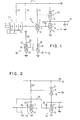
- FIG. 1 there is shown a schematic diagram of TRANSISTOR-TRANSISTOR LOGIC (TTL) gate 1 which utilizes a current mirror circuit to prevent saturation of the inverter transistor thereof without simultaneously limiting the ability of its output transistor to sink high currents.
- logic gate 1 includes a plurality of transistors T1- T 6 all of which are in NPN bipolar transistors. All of these transistors are fabricated using techniques well known to those skilled in the semiconductor fabrication arts. In the integrated circuit environment, a plurality of such devices would be interconnected in a desired way to provide a given logic function in a well known manner. Since the fabrication process forms no part of the present invention, let it suffice to say that the fabrication techniques are within the purview of those skilled in the fabrication of semiconductor integrated circuits.
- logic gate 1 includes a multi-emitter input transistor Tl which is operated under conditions of controlled saturation by shorting one of the emitter inputs 2 to the base 3 of transistor Tl.
- the collector 4 of transistor Tl is connected in parallel to the base 5 of inverter transistor T2 and base 6 of output transistor T3.
- Collector 7 of transistor T2 is connected to the base 8 of pull-up transistor T4.
- a power supply, VB is connected directly to collector 9 of transistor T4 and to base 8 of transistor T4 and collector 7 of transistor T2 via a resistor R3 and to base 3 transistor Tl via a resistor Rl.
- Emitter 10 of transistor T4 is connected directly to collector 11 of transistor T3. and to an output terminal 12.
- Emitter 13 of transistor T3 is grounded.
- Emitter 14 of inverter transistor T2 instead of being grounded has usually been done by the prior art, is connected to a current mirror circuit 15, which is comprised of NPN transistors T5, T6.
- emitter 14 of transistor T2 is connected to the collector 16 of transistor T5.
- Transistor T6 which maybe identical to transistor T5 has its collector 17 connected via a resistor R4 to voltage source VB.
- Bases 18, 19 of transistors T5, T6, respectively, are connected together and the emitters 20, 21 of transistors T5, T6 respectively, are both grounded.
- collector 17 of transistor T6 is shorted to base 19 thereof by interconnection 22.
- Output capacitor C is shown in FIG. 1 connected between output terminal 12 and ground.
- Output transistor T3 has an anti-saturation clamping diode 23 connected between its base 6 and collector 11.
- an optional resistor R2 shown connected in parallel with resistor Rl may be utilized to increase the amount of current supplied to the base of output transistor T3.
- the above described circuit achieves a reduction in power consumption and high speed switching of output transistor T3 by simultaneously controlling the current in inverter transistor T2 such that transistor T2 is kept out of saturation and by providing a much higher current to base 6 of output transistor T3 causing it to switch at high speed.
- transistor T4 Prior to the switching of transistors T2, T3, pull-up transistor T4 is in a conductive state and output capacitance C is charged to the voltage VB via conucting transistor T4.
- devices T2, T 3 are rendered conductive by the appearance of current on their bases, transistor T4 is rendered nonconductive and output capacitance C discharges through the now conducting output transistor T3.
- the maximum current that output transistor T3 can sink is its DC base current multiplied by the current gain of output transistor T3.
- the characteristics of transistors T2, T3 are substantially identical, they will share the available base current and the switching of transistor T3 will be relatively slow compared to what it could be if a higher base current were available to it.
- transistor T2 can carry a certain current and requires a certain base current which is a function of the base-emitter voltage drop of transistor T2. Without any external limitation, a rather high current could flow through transistor T2 requiring a rather high base current which, in turn, would not be available as driving base current for output transistor T3.
- the current flow through transistor T2 is controlled by the use of current mirror circuit 15 operating in a known way. Thus, when transistor T2 is conducting, the amount of current flowing in it is controlled by the amount of current flowing in resistor R4 which, in turn, controls the current which flows in transistor T5.
- transistor T2 When transistor T2 is in a nonconducting state, the characteristic of current mirror circuit 15 is such that the current in transistor T5 drops practically to zero with a small change in its base-collector voltage.
- transistor T5 When transistor T5 becomes nonconducting, the current flowing in resistor R4 passes to ground via the base-emitter diodes of transistors T5, T6.
- FIG. 2 there is shown a schematic diagram of that portion of FIG. 1 which includes transistors T2, T3 and T4.
- Input transistor Tl if it were shown in FIG. 2, would be connected to base 5 of transistor T2 in the same manner as shown in FIG. 1.
- resistor Rl if it were shown, would be connected in the same manner to base 3 of transistor Tl and voltage source VB as it is shown in FIG. 1.
- Resistor R2 would be similarly connected in FIG. 2 as shown in FIG. 1.
- FIG. 2 current mirror circuit 15 has been eliminated and emitter 14 of transistor T2 is connected directly to ground.
- An antisaturation clamping diode 24 is shown in FIG. 2, connected between base 5 and collector 7 of transistor T2.
- a resistor Rb is shown connected in series with base 5 of transistor T2.
- a direct connection 25 is shown which is connected to collector 4 of input transistor Tl and base 6 of output transistor T3.
- a speed-up capacitor Cb is shown connected in parallel with resistor Rb.
- circuit of FIG. 2 is identical with the circuit of FIG. 1.
- antisaturation clamp diode 24 prevents transistor T2 from going into heavy saturation in the usual manner.
- the amount of base current applied to base 5 of transistor T2 is directly limited by resistor Rb providing a higher proporational share of the available base current to the base of output transistor T3.
- output transistor T3 can sink a higher current and, output capacitance C discharges through it at high speed.
- transistor T2 is a function of its base current
- the current in transistor T2 is limited. Also, because the transistor T 2 is kept out of saturation a result similar to that achieved by the circuit of FIG. 1 is achieved by the circuit of FIG. 2.
- Table I shows typical values for the various components shown in FIGS. 1, 2.
Landscapes
- Engineering & Computer Science (AREA)
- Physics & Mathematics (AREA)
- Computer Hardware Design (AREA)
- Computing Systems (AREA)
- General Engineering & Computer Science (AREA)
- Mathematical Physics (AREA)
- Power Engineering (AREA)
- Logic Circuits (AREA)
- Electronic Switches (AREA)
Applications Claiming Priority (2)
| Application Number | Priority Date | Filing Date | Title |
|---|---|---|---|
| US06/282,110 US4458162A (en) | 1981-07-10 | 1981-07-10 | TTL Logic gate |
| US282110 | 1981-07-10 |
Publications (3)
| Publication Number | Publication Date |
|---|---|
| EP0069853A2 true EP0069853A2 (de) | 1983-01-19 |
| EP0069853A3 EP0069853A3 (en) | 1984-05-16 |
| EP0069853B1 EP0069853B1 (de) | 1986-03-12 |
Family
ID=23080143
Family Applications (1)
| Application Number | Title | Priority Date | Filing Date |
|---|---|---|---|
| EP82104710A Expired EP0069853B1 (de) | 1981-07-10 | 1982-05-28 | TTL logisches Tor |
Country Status (4)
| Country | Link |
|---|---|
| US (1) | US4458162A (de) |
| EP (1) | EP0069853B1 (de) |
| JP (1) | JPS5810927A (de) |
| DE (1) | DE3269791D1 (de) |
Cited By (1)
| Publication number | Priority date | Publication date | Assignee | Title |
|---|---|---|---|---|
| EP0219040A3 (en) * | 1985-10-18 | 1987-07-01 | International Business Machines Corporation | Circuitry for the speeding-up of up-going transitions in ttl or dtl circuits under high capacitive load |
Families Citing this family (7)
| Publication number | Priority date | Publication date | Assignee | Title |
|---|---|---|---|---|
| US4536664A (en) * | 1983-02-16 | 1985-08-20 | Texas Instruments Incorporated | A high speed, non-inverting circuit for providing an interface between TTL logic gates and Schottky transistor logic gates |
| US4634898A (en) * | 1983-11-22 | 1987-01-06 | Monolithic Memories, Inc. | TTL buffer circuit incorporating active pull-down transistor |
| US4577125A (en) * | 1983-12-22 | 1986-03-18 | Advanced Micro Devices, Inc. | Output voltage driver with transient active pull-down |
| US4893032A (en) * | 1987-03-23 | 1990-01-09 | International Business Machines Corp. | Non-saturating temperature independent voltage output driver with adjustable down level |
| US5089724A (en) * | 1990-11-30 | 1992-02-18 | International Business Machines Corporation | High-speed low-power ECL/NTL circuits with AC-coupled complementary push-pull output stage |
| DE69205625T2 (de) * | 1991-05-31 | 1996-06-20 | Fuji Kiko Kk | Sitzgleitvorrichtung. |
| US5210447A (en) * | 1991-10-30 | 1993-05-11 | International Business Machines Corporation | Word decoder with sbd-tx clamp |
Family Cites Families (11)
| Publication number | Priority date | Publication date | Assignee | Title |
|---|---|---|---|---|
| US3303355A (en) * | 1963-06-27 | 1967-02-07 | John A Kolling | Or-inverter |
| US3564281A (en) * | 1966-12-23 | 1971-02-16 | Hitachi Ltd | High speed logic circuits and method of constructing the same |
| US3571616A (en) * | 1969-06-18 | 1971-03-23 | Honeywell Inc | Logic circuit |
| US3769530A (en) * | 1969-07-11 | 1973-10-30 | Nat Semiconductor Corp | Multiple emitter transistor apparatus |
| US3629609A (en) * | 1970-02-20 | 1971-12-21 | Bell Telephone Labor Inc | Ttl input array with bypass diode |
| US3641368A (en) * | 1970-08-10 | 1972-02-08 | Rca Corp | Logic circuit which turns on and off rapidly |
| US3867644A (en) * | 1974-01-07 | 1975-02-18 | Signetics Corp | High speed low power schottky integrated logic gate circuit with current boost |
| US3934157A (en) * | 1974-09-23 | 1976-01-20 | Bell Telephone Laboratories, Incorporated | TTL circuit |
| US4092551A (en) * | 1976-05-20 | 1978-05-30 | International Business Machines Corporation | A.C. powered speed up circuit |
| JPS5367341A (en) * | 1976-11-27 | 1978-06-15 | Mitsubishi Electric Corp | Output circuit |
| US4194131A (en) * | 1978-05-30 | 1980-03-18 | National Semiconductor Corporation | Tristate logic buffer circuit with enhanced dynamic response |
-
1981
- 1981-07-10 US US06/282,110 patent/US4458162A/en not_active Expired - Lifetime
-
1982
- 1982-05-20 JP JP57084100A patent/JPS5810927A/ja active Granted
- 1982-05-28 DE DE8282104710T patent/DE3269791D1/de not_active Expired
- 1982-05-28 EP EP82104710A patent/EP0069853B1/de not_active Expired
Cited By (1)
| Publication number | Priority date | Publication date | Assignee | Title |
|---|---|---|---|---|
| EP0219040A3 (en) * | 1985-10-18 | 1987-07-01 | International Business Machines Corporation | Circuitry for the speeding-up of up-going transitions in ttl or dtl circuits under high capacitive load |
Also Published As
| Publication number | Publication date |
|---|---|
| EP0069853B1 (de) | 1986-03-12 |
| US4458162A (en) | 1984-07-03 |
| JPH0213862B2 (de) | 1990-04-05 |
| DE3269791D1 (en) | 1986-04-17 |
| EP0069853A3 (en) | 1984-05-16 |
| JPS5810927A (ja) | 1983-01-21 |
Similar Documents
| Publication | Publication Date | Title |
|---|---|---|
| US3868517A (en) | Low hysteresis threshold detector having controlled output slew rate | |
| JPH02179120A (ja) | 負荷制御エミッタ結合論理過渡ドライバ | |
| US4897564A (en) | BICMOS driver circuit for high density CMOS logic circuits | |
| US5089724A (en) | High-speed low-power ECL/NTL circuits with AC-coupled complementary push-pull output stage | |
| JPH0216588B2 (de) | ||
| US4804868A (en) | BiMOS logical circuit | |
| US4112314A (en) | Logical current switch | |
| EP0069853B1 (de) | TTL logisches Tor | |
| US4376900A (en) | High speed, non-saturating, bipolar transistor logic circuit | |
| US4039867A (en) | Current switch circuit having an active load | |
| US3769524A (en) | Transistor switching circuit | |
| US4623803A (en) | Logic level translator circuit for integrated circuit semiconductor devices having transistor-transistor logic output circuitry | |
| US5059827A (en) | ECL circuit with low voltage/fast pull-down | |
| US4709166A (en) | Complementary cascoded logic circuit | |
| US3571616A (en) | Logic circuit | |
| US4531067A (en) | Push-pull Darlington current sink (PPDCS) logic circuit | |
| US3358154A (en) | High speed, low dissipation logic gates | |
| EP0285157B1 (de) | Tri-state-Ausgangsschaltung | |
| US4851715A (en) | Schottky-clamped transistor logic buffer circuit | |
| EP0028292B1 (de) | Aus NPN-Transistoren aufgebaute Treiber- und Logikschaltung | |
| JPH02248117A (ja) | 高速度のスイッチング速度を有するttlコンパチブル出力回路 | |
| US4868904A (en) | Complementary noise-immune logic | |
| KR0165986B1 (ko) | BiCMOS 논리 회로 | |
| US4675554A (en) | NPN transient driver circuit | |
| US4585959A (en) | Tri-state logic gate having reduced Miller capacitance |
Legal Events
| Date | Code | Title | Description |
|---|---|---|---|
| PUAI | Public reference made under article 153(3) epc to a published international application that has entered the european phase |
Free format text: ORIGINAL CODE: 0009012 |
|
| AK | Designated contracting states |
Designated state(s): DE FR GB |
|
| 17P | Request for examination filed |
Effective date: 19830519 |
|
| PUAL | Search report despatched |
Free format text: ORIGINAL CODE: 0009013 |
|
| RHK1 | Main classification (correction) |
Ipc: H03K 19/013 |
|
| AK | Designated contracting states |
Designated state(s): DE FR GB |
|
| GRAA | (expected) grant |
Free format text: ORIGINAL CODE: 0009210 |
|
| AK | Designated contracting states |
Kind code of ref document: B1 Designated state(s): DE FR GB |
|
| REF | Corresponds to: |
Ref document number: 3269791 Country of ref document: DE Date of ref document: 19860417 |
|
| ET | Fr: translation filed | ||
| PLBE | No opposition filed within time limit |
Free format text: ORIGINAL CODE: 0009261 |
|
| STAA | Information on the status of an ep patent application or granted ep patent |
Free format text: STATUS: NO OPPOSITION FILED WITHIN TIME LIMIT |
|
| 26N | No opposition filed | ||
| PGFP | Annual fee paid to national office [announced via postgrant information from national office to epo] |
Ref country code: FR Payment date: 19910430 Year of fee payment: 10 |
|
| PGFP | Annual fee paid to national office [announced via postgrant information from national office to epo] |
Ref country code: GB Payment date: 19920409 Year of fee payment: 11 |
|
| PGFP | Annual fee paid to national office [announced via postgrant information from national office to epo] |
Ref country code: DE Payment date: 19920523 Year of fee payment: 11 |
|
| PG25 | Lapsed in a contracting state [announced via postgrant information from national office to epo] |
Ref country code: FR Effective date: 19930129 |
|
| REG | Reference to a national code |
Ref country code: FR Ref legal event code: ST |
|
| PG25 | Lapsed in a contracting state [announced via postgrant information from national office to epo] |
Ref country code: GB Effective date: 19930528 |
|
| GBPC | Gb: european patent ceased through non-payment of renewal fee |
Effective date: 19930528 |
|
| PG25 | Lapsed in a contracting state [announced via postgrant information from national office to epo] |
Ref country code: DE Effective date: 19940201 |