EP0070158A2 - Spannungsspitzen-Begrenzerschaltung geringen Verlustes für Leistungsschalttransistoren - Google Patents
Spannungsspitzen-Begrenzerschaltung geringen Verlustes für Leistungsschalttransistoren Download PDFInfo
- Publication number
- EP0070158A2 EP0070158A2 EP82303593A EP82303593A EP0070158A2 EP 0070158 A2 EP0070158 A2 EP 0070158A2 EP 82303593 A EP82303593 A EP 82303593A EP 82303593 A EP82303593 A EP 82303593A EP 0070158 A2 EP0070158 A2 EP 0070158A2
- Authority
- EP
- European Patent Office
- Prior art keywords
- transistor
- capacitor
- base
- resistor
- diode
- Prior art date
- Legal status (The legal status is an assumption and is not a legal conclusion. Google has not performed a legal analysis and makes no representation as to the accuracy of the status listed.)
- Granted
Links
Images


Classifications
-
- H—ELECTRICITY
- H02—GENERATION; CONVERSION OR DISTRIBUTION OF ELECTRIC POWER
- H02M—APPARATUS FOR CONVERSION BETWEEN AC AND AC, BETWEEN AC AND DC, OR BETWEEN DC AND DC, AND FOR USE WITH MAINS OR SIMILAR POWER SUPPLY SYSTEMS; CONVERSION OF DC OR AC INPUT POWER INTO SURGE OUTPUT POWER; CONTROL OR REGULATION THEREOF
- H02M1/00—Details of apparatus for conversion
- H02M1/32—Means for protecting converters other than automatic disconnection
- H02M1/34—Snubber circuits
-
- H—ELECTRICITY
- H02—GENERATION; CONVERSION OR DISTRIBUTION OF ELECTRIC POWER
- H02M—APPARATUS FOR CONVERSION BETWEEN AC AND AC, BETWEEN AC AND DC, OR BETWEEN DC AND DC, AND FOR USE WITH MAINS OR SIMILAR POWER SUPPLY SYSTEMS; CONVERSION OF DC OR AC INPUT POWER INTO SURGE OUTPUT POWER; CONTROL OR REGULATION THEREOF
- H02M1/00—Details of apparatus for conversion
- H02M1/08—Circuits specially adapted for the generation of control voltages for semiconductor devices incorporated in static converters
-
- H—ELECTRICITY
- H02—GENERATION; CONVERSION OR DISTRIBUTION OF ELECTRIC POWER
- H02M—APPARATUS FOR CONVERSION BETWEEN AC AND AC, BETWEEN AC AND DC, OR BETWEEN DC AND DC, AND FOR USE WITH MAINS OR SIMILAR POWER SUPPLY SYSTEMS; CONVERSION OF DC OR AC INPUT POWER INTO SURGE OUTPUT POWER; CONTROL OR REGULATION THEREOF
- H02M7/00—Conversion of AC power input into DC power output; Conversion of DC power input into AC power output
- H02M7/42—Conversion of DC power input into AC power output without possibility of reversal
- H02M7/44—Conversion of DC power input into AC power output without possibility of reversal by static converters
- H02M7/48—Conversion of DC power input into AC power output without possibility of reversal by static converters using discharge tubes with control electrode or semiconductor devices with control electrode
- H02M7/53—Conversion of DC power input into AC power output without possibility of reversal by static converters using discharge tubes with control electrode or semiconductor devices with control electrode using devices of a triode or transistor type requiring continuous application of a control signal
- H02M7/537—Conversion of DC power input into AC power output without possibility of reversal by static converters using discharge tubes with control electrode or semiconductor devices with control electrode using devices of a triode or transistor type requiring continuous application of a control signal using semiconductor devices only, e.g. single switched pulse inverters
- H02M7/5387—Conversion of DC power input into AC power output without possibility of reversal by static converters using discharge tubes with control electrode or semiconductor devices with control electrode using devices of a triode or transistor type requiring continuous application of a control signal using semiconductor devices only, e.g. single switched pulse inverters in a bridge configuration
-
- H—ELECTRICITY
- H03—ELECTRONIC CIRCUITRY
- H03K—PULSE TECHNIQUE
- H03K17/00—Electronic switching or gating, i.e. not by contact-making and –breaking
- H03K17/04—Modifications for accelerating switching
- H03K17/042—Modifications for accelerating switching by feedback from the output circuit to the control circuit
- H03K17/04213—Modifications for accelerating switching by feedback from the output circuit to the control circuit in bipolar transistor switches
-
- H—ELECTRICITY
- H03—ELECTRONIC CIRCUITRY
- H03K—PULSE TECHNIQUE
- H03K17/00—Electronic switching or gating, i.e. not by contact-making and –breaking
- H03K17/08—Modifications for protecting switching circuit against overcurrent or overvoltage
- H03K17/081—Modifications for protecting switching circuit against overcurrent or overvoltage without feedback from the output circuit to the control circuit
- H03K17/0814—Modifications for protecting switching circuit against overcurrent or overvoltage without feedback from the output circuit to the control circuit by measures taken in the output circuit
- H03K17/08146—Modifications for protecting switching circuit against overcurrent or overvoltage without feedback from the output circuit to the control circuit by measures taken in the output circuit in bipolar transistor switches
-
- H—ELECTRICITY
- H02—GENERATION; CONVERSION OR DISTRIBUTION OF ELECTRIC POWER
- H02M—APPARATUS FOR CONVERSION BETWEEN AC AND AC, BETWEEN AC AND DC, OR BETWEEN DC AND DC, AND FOR USE WITH MAINS OR SIMILAR POWER SUPPLY SYSTEMS; CONVERSION OF DC OR AC INPUT POWER INTO SURGE OUTPUT POWER; CONTROL OR REGULATION THEREOF
- H02M1/00—Details of apparatus for conversion
- H02M1/0003—Details of control, feedback or regulation circuits
- H02M1/0006—Arrangements for supplying an adequate voltage to the control circuit of converters
-
- H—ELECTRICITY
- H02—GENERATION; CONVERSION OR DISTRIBUTION OF ELECTRIC POWER
- H02M—APPARATUS FOR CONVERSION BETWEEN AC AND AC, BETWEEN AC AND DC, OR BETWEEN DC AND DC, AND FOR USE WITH MAINS OR SIMILAR POWER SUPPLY SYSTEMS; CONVERSION OF DC OR AC INPUT POWER INTO SURGE OUTPUT POWER; CONTROL OR REGULATION THEREOF
- H02M1/00—Details of apparatus for conversion
- H02M1/32—Means for protecting converters other than automatic disconnection
- H02M1/34—Snubber circuits
- H02M1/348—Passive dissipative snubbers
-
- H—ELECTRICITY
- H03—ELECTRONIC CIRCUITRY
- H03K—PULSE TECHNIQUE
- H03K2217/00—Indexing scheme related to electronic switching or gating, i.e. not by contact-making or -breaking covered by H03K17/00
- H03K2217/0036—Means reducing energy consumption
-
- H—ELECTRICITY
- H03—ELECTRONIC CIRCUITRY
- H03K—PULSE TECHNIQUE
- H03K2217/00—Indexing scheme related to electronic switching or gating, i.e. not by contact-making or -breaking covered by H03K17/00
- H03K2217/0081—Power supply means, e.g. to the switch driver
Definitions
- the subject invention generally relates to circuits employing power switching transistors such as inverters, choppers and the like, and more particularly to improvements in snubber circuits for such power switching transistors.
- the conventional method for controlling the load line of bipolar transistors is to connect a polarized snubber from the collector to the emitter as shown in FIGURE 1. More specifically, (an NPN) transistor 11 is controlled by a base driver circuit 12 to alternately turn on and off so as to permit current to flow or block the flow of current through the load 13, (here represented as an inductor).
- the snubber circuit consists of a diode 14 and a capacitor 15 connected in series between a collector terminal and an emitter terminal of transistor 11 and a resistor 16 connected between the junction of a diode 14 and a capacitor 15 and the collector terminal of transistor 11.
- a base driver power supply 17 (represented as a battery) must provide sufficient voltage to supply the base boost required to turn the transistor 11 on.
- the basic purpose of the snubber circuit consisting of the diode 14, the capacitor 15 and the resistor 16 is to protect the transistor 11 at turn-off by transferring the collector current to the capacitor 15 via the diode 14 before the transistor voltage is allowed to rise. This reduces switching power losses in the transistor 11.
- the snubber capacitor 15 must be discharged prior to any subsequent turn-off of the transistor 11. This discharge is performed by the transistor 11 when it turns on through the resistor 16.
- FIGURE 2 A collector current waveform typically occurring in a push-pull circuit is illustrated in FIGURE 2.
- the high peak collector current at turn-on requires more base current drive to maintain saturation.
- the base current drive requirement is further aggravated by the fact that most power transistor current gains (p) drop off significantly at high collector current values.
- the peaking of the base drive current necessary to compensate for the low gain at high collector current is usually provided by a parallel RC circuit in series with the base terminal.
- the foregoing and other objects of the invention are achieved by a modification of the conventional snubber circuitry so that the snubber capacitor is discharged through the base turn-on circuit rather than through the collector of the power switching transistors. Since the invention uses the energy stored in the snubber capacitor to provide the additional power required for the base drive circuitry, the base current boost compensates for the increased collector current which causes the fall off of current gain at the moment of turn-on. All of the base boost power is derived from the snubber energy, which is usually dissipated as heat, thereby increasing the overall system efficiency. The effective snubber power source is combined with the base turn-on power supply, both of which are referenced to the transistor emitter, to provide the base boost power.
- The-voltage level of the base turn-on power supply is usually dictated by stray inductance in the base circuit and the rise time required to minimize losses at turn-on. This voltage is considerably higher than that required to sustain saturation, and excess power is consumed in the base circuit most of the on-time. In simple drive circuits, the higher drive level stores excess charge in the base causing longer turn-off delays.
- a high voltage source (the snubber charge) is available to supply all of the energy required for turning on the transistor.
- the voltage level of the base turn-on supply can be reduced to a level just great enough to sustain the base drive level after the transistor saturates.
- FIGURE 3 of the drawings wherein like reference numerals represent the same or similar elements as shown in the conventional snubber circuit of FIGURE 1. More specifically, the resistor 16 is now connected between the junction of diode 14 and capacitor 15 and the base driver 12. Discharge of the snubber capacitor 15 is now through the base driver 12 instead of the collector to emitter path of transistor 11. A diode 18 is inserted between the power supply 17 and the base driver 12 to isolate the power supply 17 from the high voltage discharge of snubber capacitor 15. Since all of the base boost is now supplied by the discharge of snubber capacitor 15, the power supply 17 can be substantially smaller than the power supply 17 used in the conventional circuit shown in" FIGURE 1. The resulting collector current waveform is shown in FIGURE 4. It will be observed that the peak collector current, I , at turn-on is reduced requiring less base drive current peaking to keep the transistor 11 in saturation at turn-on.
- the switching power transistor 111 is represented as a Darlington pair which, depending on the specific application, may comprise any number of transistors connected to form a switch.
- the snubber circuit consists of diode 114 and capacitor 115 connected betwen the collector and emitter terminals of transistor 111 and resistor 116 connected at one end to the junction of capacitor 115 and diode 114 and at the other end to the junction of a base driver and turn-on switch transistor 121 and an isolation diode 118.
- the transistor 121 provides the base current drive to transistor 111 through a current limiting resistor 122.
- the transistor 121 is depicted as an NPN bipolar transistor but, depending on the specific application, can be any number or type of device connected to form a single pole switch.
- a turn-off circuit 123 is provided to turn off and hold off the power switching transistor 111.
- a control signal circuit 124' is required to provide the appropriate signals to operate the turn-on switch transistor 121 and turn-off circuit 123.
- the specific mechanizations of the turn-off circuit 123 and the control signal circuit 124 are irrelevant to the performance of the invention. Any mechanization that performs the desired functions would be well within the purview of one skilled in the art, having the knowledge of the application herewith presented.
- the snubber capacitor 115 stays charged since diode 118 is reverse biased and transistor 121 is maintained off by the control signal circuit. During this period the control signal keeps the turn-off circuit 124 enabled which maintains the power switching transistor 111 in its off state.
- the control signal circuit disables the turn-off circuit 123 and provides enough base drive current to transistor 121 to cause it to saturate.
- transistor 121 turns on it causes the snubber capacitor to discharge through resistors 116 and 122 into the base-emitter junction of switching power transistor 111.
- diode 118 becomes forward biased and provides the remaining or steady state base drive current from supply 117. At this point no more current flows from the snubber capacitor 115 and its residual charge remains at a potential which is approximately the same as the power supply 117 potential.
- control signal circuitry 124 removes the base drive to :ransistor 121 and enables the turn-off circuit 123. This action disconnects resistor 116 from the discharge path and turns off transistor 111. As the switching power transistor 111 turns off, the capacitor 115 is recharged through diode 114 as would a conventional snubber. This new charge is maintained on the snubber capacitor 115 until the next subsequent turn on of the switching power transistor 111 causing the previously described sequence to be repeated.
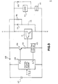
- FIGURE 5 shows a specific preferred embodiment of the invention.
- the switching power transistor 111 is represented as a Darlington pair which, depending on the specific application, may comprise a plurality of paralleled output transistors driven by one or more parallel driver transistors.
- the snubber circuit consists of diode 114 and snubber capacitor 115 connected in series between the collector terminal and the emitter terminal of the switching power transistor 111 and resistor 116 connected at one end to the junction of diode 114 and snubber capacitor 115.
- the load 113 and power supply 119 is connected between the collector terminal and the emitter terminal of the switching power transistor 111.
- the power supply for the base driver circuit is referenced to the emitter terminal of the switching power transistor 111 and is connected between terminals 117a and 117b. More specifically, terminal 117a has a voltage +V applied to it, and terminal 117b has a voltage -V applied to it. Intermediate of the voltages applied to the terminals 117a and 117b is a line connected to the emitter terminal of the switching power transistor 111 at zero volts.
- a voltage dropping resistor 121, a Zener diode 122 and a capacitor 123 are used to establish a stable supply voltage for an opto-coupler 124.
- a switching control signal of a pulse width modulated type having relatively fast rise and fall time is supplied from a source (not shown) of a type well known in the art and is applied to input terminals 125a and 125b of the opto-coupler to control the turn-on and turn-off of the switching power transistor 111.
- the output of the opto-coupler 124 which . is referenced to the zero volt line by a resistor 126 is supplied to the input of a logic gate 127.
- the logic gate 127 is a power NAND buffer with-open collector outputs referenced to the -V terminal 117b.
- the output of logic gate 127 is supplied to the input of a second logic gate 128, also a NAND buffer, and the output of logic gate 127 is clamped at zero volts maximum potential by a diode 129 to protect the inputs of the second logic gate 128.
- An output terminal of logic gate 128 is connected to a gate terminal of a power field effect transistor (FET) 130.
- the FET 130 operates as a switch to control the power transistor 111.
- FET 130 has a drain terminal connected to the base terminal of transistor 111 and a source terminal connected through a current limiting resistor 143 to the -V terminal 117b.
- a base current source comprising four paralleled transistor stages 134a, 134b, 134c and 134d is connected between the base terminal of transistor 111 and the +V terminal 117a.
- Each of the transistors 134 has an emitter terminal connected through a corresponding emitter resistor 146 to the base terminal of transistor lll.
- a collector terminal of each transistor 134 is connected to a common junction and thence through a reverse current blocking-diode 118 to +V terminal 117a.
- Turn-off time of transistor 111 is reduced by a charge-sweeping capacitor 140 serially connected with a damping resistor 141 through the drain-source terminal of FET 130 between the base terminal and emitter terminal of transistor 111.
- a charge-sweeping capacitor 140 serially connected with a damping resistor 141 through the drain-source terminal of FET 130 between the base terminal and emitter terminal of transistor 111.
- the resistor 141 may have a value of less than one ohm serves to damp oscillatory currents.
- a resistor 142 provides a leakage current path for the base junction of transistor 111 in the event the high voltage source 119 is energized while the low voltage base drive power source 117 is de-energized.
- a gating circuit comprising a FET 137 and a FET 136 controls the base drive current supplied to base current source transistors 134.
- FET 137 has a drain terminal connected to +V terminal 117a and a source terminal connected through a current limit resistor 131 to the output terminal of logic gate 127.
- a gate terminal of FET 137 is connected through a current limiting resistor 145 to a junction intermediate a diode 139 and a capacitor 138.
- the diode 139 and capacitor 138 are serially connected between the drain and source terminals of FET 137 with the diode 139 being poled such that capacitor 138 can be charged from the +V terminal 117a.
- Drive current is coupled from the source terminal of FET 137 through a speed-up capacitor 133 and parallel connected current setting resistor 132 to a base terminal of transistors 134.
- the FET 137 is controlled by the FET 136 which FET 136 is connected between the gate and source terminals of FET 137.
- FET 136 is a junction FET such that its source to drain impedance is relatively low in the absence of any reverse gate bias.
- FET 136 is forced into non-conduction by a signal from logic gate 128 which is coupled through a diode 135 to the gate terminal of F E T 136.
- a pull-up resistor 144 assures that diode 135 is reverse biased when the output of gate 128 becomes open- circuit.
- the first logic gate 127 With no control signal applied to the opto-coupler 124, the first logic gate 127 is saturated, and the second logic gate 128 is open. This allows the gate potential of the power FET 130 to be pulled up to the +V supply, turning it on.
- the output of the first logic gate 127 through the resistor 131 and the parallel connection of resistor 132 and capacitor 133 keeps the bases of the four parallel driver transistor stages 134a, 134b, 134c, and 134d at a negative potential and provides a leakage path for the driver stages.
- the logic states of logic gates 127 and 128 maintain a reverse bias across diode 135 resulting in a zero gate bias for transistor 136.
- the zero gate bias maintains transistor 136 on which keeps the V-MOS driver FET 137 in the off state.
- a switching current is applied to the input terminals 125a and 125b of the opto-coupler 124. This causes the logic gate outputs to change states.
- the output of logic gate 128 is pulled down to the -V supply voltage which immediately turns off transistor 130 and applies a negative gate bias to transistor 136 which turns it off.
- transistor 136 opens, some of the charge on capacitor 138 is dumped into the input capacitance of transistor 137 turning it on.
- transistor 137 turns on, its gate is boot strapped above the supply by means of diode 139 which is reversed biased, holding it on.
- Capacitor 133 is a speed-up capacitor which bypasses the current setting resistor 132 to provide increased base current to the driver stages 134a, 134b, 134c and 134d at turn-on.
- the time constant of this speed-up circuit is set equal or slightly longer than the discharge time constant of the snubber. This improves the turn-on rise time of the switching power transistor 111 and reduces dissipation in the driver transistors 134a-d.
- the snubber capacitor 115 is discharged via resistor 116 through the driver stages 134a, 134b, 134c, and 134d and the base-emitter junctions of the switching power transistor 111. While the snubber capacitor 115 is being discharged, the diode 118 is reverse biased. As the charge decays, the source of base current transfers from the snubber capacitor 115 to the +V. supply voltage.
- Capacitor 140 connected in the source circuit of transistor 130 provides the current path during the turn-off transition. This capacitor is recharged through resistor 141 while the switching power transistor 111 is on and the transistor 130 is off.
- the snubber discharge time constant must be picked so that the capacitor 115 is always discharged to the bias supply voltage before the transistor 111 is turned off again to ensure the same snubbing capability.
- FIGURES 6A and 6B show basic power switch circuits duplicated to form push-pull power switch.
- Each base driver 212a and 212b is supplied with a switching signal on alternate half cycles.
- the configuration shown in FIGURES 6A and 6B is a half bridge, and it is possible to provide a full bridge configuration by simply replacing the supply center tap with two more power switching circuits.
- Such push-pull configurations are used in pulse width modulation (PWM) systems.
- PWM pulse width modulation
- the load appears as a constant current source, assuming that the modulation frequency is much greater than the fundamental frequency.
- the load current is alternately switched between the corresponding transistor and its clamp diode path 220 while the alternate transistor and clamp diode 220 are not conducting.
- the alternate snubber In a push-pull power switch using conventional snubber circuits as represented in FIGURE 6A, the alternate snubber is still connected to the load and is discharged during every PWM cycle through the discharge resistor into the load every free wheeling period.
- the modulated transistor turns back on, high peak collector currents flow through the alternate snubber circuit until it regains its charge. This causes the discharge resistor to dissipate high power during both half cycles of the fundamental-frequency.
- the high peak charging currents dictate the use of overrated snubber capacitors.
- FIGURE 6B illustrates the snubber capacitor is automatically disconnected from the load on one half cycle, except for leakage currents through the snubber diode 214.
- the high peak currents are eliminated from both the alternate snubber capacitor and the modulated transistor.
- the snubber resistor 216 only dissipates power on one half cycle reducing its losses by fifty percent.
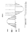
- FIGURE 8 illustrates the approximate snubber capacitor current for one PWM cycle.
- the left half of FIGURE 8 is the chopping half cycle, and the right half of FIGURE 8 is the OFF half cycle.
- the dashed sinusoidal line represents average load current.
- the pulse currents during both the chopping half cycle and the off half-cycle are characteristic of conventional snubber circuits.
- the currents shown in the OFF half cycle are eliminated with the new snubber circuit according to the present invention.
- the elimination of the large positive current spikes during the OFF half cycle reduces stress on the snubber components and the switching power transistors.
- FIGURE 6 The push-pull configuration of FIGURE 6 can be applied to a multi-phase system, an example of which is shown in FIGURE 7. More specifically, FIGURE 7 shows a three phase system which could be readily expanded to n phases. This arrangement has the same advantages as the simplified push-pull arrangement shown in FIGURE 6.
Landscapes
- Engineering & Computer Science (AREA)
- Power Engineering (AREA)
- Power Conversion In General (AREA)
- Electronic Switches (AREA)
Applications Claiming Priority (2)
| Application Number | Priority Date | Filing Date | Title |
|---|---|---|---|
| US06/283,219 US4414479A (en) | 1981-07-14 | 1981-07-14 | Low dissipation snubber for switching power transistors |
| US283219 | 1981-07-14 |
Publications (3)
| Publication Number | Publication Date |
|---|---|
| EP0070158A2 true EP0070158A2 (de) | 1983-01-19 |
| EP0070158A3 EP0070158A3 (en) | 1983-10-19 |
| EP0070158B1 EP0070158B1 (de) | 1986-05-07 |
Family
ID=23085066
Family Applications (1)
| Application Number | Title | Priority Date | Filing Date |
|---|---|---|---|
| EP82303593A Expired EP0070158B1 (de) | 1981-07-14 | 1982-07-08 | Spannungsspitzen-Begrenzerschaltung geringen Verlustes für Leistungsschalttransistoren |
Country Status (4)
| Country | Link |
|---|---|
| US (1) | US4414479A (de) |
| EP (1) | EP0070158B1 (de) |
| JP (1) | JPS5826568A (de) |
| DE (1) | DE3270984D1 (de) |
Cited By (3)
| Publication number | Priority date | Publication date | Assignee | Title |
|---|---|---|---|---|
| WO1987004024A1 (en) * | 1985-12-19 | 1987-07-02 | Italtel Società Italiana Telecomunicazioni S.P.A. | Control circuit of the power transistor in a dc/ac converter |
| EP3696976A1 (de) * | 2019-02-12 | 2020-08-19 | Bühler Motor GmbH | Energierückgewinnungsschaltung |
| US10770962B2 (en) | 2016-04-08 | 2020-09-08 | Abb Schweiz Ag | Converter cell comprising an energy converter in parallel to a clamp inductor |
Families Citing this family (23)
| Publication number | Priority date | Publication date | Assignee | Title |
|---|---|---|---|---|
| DE3240352C2 (de) * | 1982-11-02 | 1985-07-18 | Danfoss A/S, Nordborg | Elektronische Schaltvorrichtung |
| CH653495A5 (fr) * | 1983-07-05 | 1985-12-31 | Cerac Inst Sa | Circuit de commande d'un convertisseur statique. |
| US4588906A (en) * | 1984-04-25 | 1986-05-13 | The Grass Valley Group, Inc. | Regulator circuit |
| JPS61131613A (ja) * | 1984-11-29 | 1986-06-19 | Mitsubishi Electric Corp | 駆動回路 |
| US4639849A (en) * | 1985-05-08 | 1987-01-27 | International Exide Electronics/Corporation | Snubber circuit for H.F. bridge converter |
| US4654544A (en) * | 1985-11-12 | 1987-03-31 | Combustion Engineering, Inc. | Darlington transistor driver with reverse base drive current |
| US4772810A (en) * | 1986-09-30 | 1988-09-20 | Hewlett-Packard Company | Apparatus for non-dissipative switching transistor snubber |
| FR2649841B1 (fr) * | 1989-07-17 | 1994-10-14 | Sgs Thomson Microelectronics | Circuit de commande de grille d'un transistor mos |
| JP2674341B2 (ja) * | 1991-03-27 | 1997-11-12 | 三菱電機株式会社 | 電力変換装置のスナバ回路 |
| US5416361A (en) * | 1993-09-02 | 1995-05-16 | At&T Corp. | Low dissipation snubber for switching power transistor |
| US5740213A (en) * | 1994-06-03 | 1998-04-14 | Dreyer; Stephen F. | Differential charge pump based phase locked loop or delay locked loop |
| USRE36454E (en) * | 1994-11-02 | 1999-12-21 | General Electric Company | Electrical propulsion systems for a vehicle |
| US5565760A (en) * | 1994-11-02 | 1996-10-15 | General Electric Company | Electrical propulsion systems for a golf car |
| US5880513A (en) * | 1996-04-18 | 1999-03-09 | Harris Corporation | Asymmetric snubber resistor |
| JP3560432B2 (ja) * | 1996-12-18 | 2004-09-02 | 株式会社日立製作所 | Mosトランジスタの駆動装置 |
| DE19920306B4 (de) * | 1999-05-03 | 2008-02-28 | Stmicroelectronics Gmbh | Schaltungsvorrichtung zum Regeln des Stroms durch eine induktive Last |
| DE10001394A1 (de) * | 2000-01-14 | 2001-07-26 | Infineon Technologies Ag | Schaltungsanordnung zum Anlegen einer Versorgungsspannung an eine Last |
| WO2001059918A1 (fr) * | 2000-02-09 | 2001-08-16 | Mitsubishi Denki Kabushiki Kaisha | Dispositif onduleur |
| JP4682007B2 (ja) * | 2004-11-10 | 2011-05-11 | 三菱電機株式会社 | 電力用半導体装置 |
| WO2006052032A1 (ja) * | 2004-11-15 | 2006-05-18 | Kabushiki Kaisha Toshiba | 電力変換装置 |
| US9768607B2 (en) * | 2015-05-11 | 2017-09-19 | Infineon Technologies Ag | System and method for a multi-phase snubber circuit |
| TWI723320B (zh) * | 2018-01-11 | 2021-04-01 | 美商先驅能源工業公司 | 低功率pin型二極體驅動器 |
| DE102020216184A1 (de) | 2020-12-17 | 2022-06-23 | Vitesco Technologies Germany Gmbh | Galvanisch trennender Bordnetz-Gleichspannungwandler, Fahrzeugbordnetz mit Bordnetz-Gleichspannungswandler und Verfahren zum Betreiben eines galvanisch trennenden Gleichspannungwandlers |
Family Cites Families (7)
| Publication number | Priority date | Publication date | Assignee | Title |
|---|---|---|---|---|
| US3571614A (en) * | 1968-08-05 | 1971-03-23 | Hughes Aircraft Co | Transistor switch with minimized transition power absorption |
| JPS50145840A (de) * | 1974-05-11 | 1975-11-22 | ||
| JPS5718427B2 (de) * | 1974-05-29 | 1982-04-16 | ||
| US4137570A (en) * | 1977-10-31 | 1979-01-30 | Exxon Research & Engineering Co. | Waveform synthesizer |
| JPS5541167A (en) * | 1978-09-18 | 1980-03-22 | Fuji Electric Co Ltd | Snap circuit |
| JPS5745722A (en) * | 1980-09-01 | 1982-03-15 | Origin Electric Co Ltd | High-speed turn-off circuit for semiconductor switch element |
| US4365171A (en) * | 1980-12-23 | 1982-12-21 | General Electric Company | Low loss snubber circuit |
-
1981
- 1981-07-14 US US06/283,219 patent/US4414479A/en not_active Expired - Fee Related
-
1982
- 1982-07-08 EP EP82303593A patent/EP0070158B1/de not_active Expired
- 1982-07-08 DE DE8282303593T patent/DE3270984D1/de not_active Expired
- 1982-07-13 JP JP57120700A patent/JPS5826568A/ja active Granted
Cited By (3)
| Publication number | Priority date | Publication date | Assignee | Title |
|---|---|---|---|---|
| WO1987004024A1 (en) * | 1985-12-19 | 1987-07-02 | Italtel Società Italiana Telecomunicazioni S.P.A. | Control circuit of the power transistor in a dc/ac converter |
| US10770962B2 (en) | 2016-04-08 | 2020-09-08 | Abb Schweiz Ag | Converter cell comprising an energy converter in parallel to a clamp inductor |
| EP3696976A1 (de) * | 2019-02-12 | 2020-08-19 | Bühler Motor GmbH | Energierückgewinnungsschaltung |
Also Published As
| Publication number | Publication date |
|---|---|
| DE3270984D1 (en) | 1986-06-12 |
| JPH0328847B2 (de) | 1991-04-22 |
| EP0070158A3 (en) | 1983-10-19 |
| EP0070158B1 (de) | 1986-05-07 |
| US4414479A (en) | 1983-11-08 |
| JPS5826568A (ja) | 1983-02-17 |
Similar Documents
| Publication | Publication Date | Title |
|---|---|---|
| US4414479A (en) | Low dissipation snubber for switching power transistors | |
| US5281862A (en) | Power MOSFET driver with cross-conduction current reduction | |
| US4445055A (en) | Circuit arrangement for controlling a power field-effect switching transistor | |
| US4885486A (en) | Darlington amplifier with high speed turnoff | |
| US4706177A (en) | DC-AC inverter with overload driving capability | |
| US4360744A (en) | Semiconductor switching circuits | |
| US4356416A (en) | Voltage controlled non-saturating semiconductor switch and voltage converter circuit employing same | |
| EP0763882B1 (de) | Lasttreibervorrichtung | |
| US4590395A (en) | FET-bipolar drive circuit | |
| CN111884491A (zh) | 一种具有能量回收功能的驱动电路及开关电源 | |
| US4725741A (en) | Drive circuit for fast switching of Darlington-connected transistors | |
| EP0318812B1 (de) | Mit niedriger Spannung gespeiste Treiberschaltung für elektronische Vorrichtungen | |
| US4777386A (en) | Driver circuit for a bipolar Darlington power transistor | |
| EP1596496B1 (de) | Ansteuerschaltung für einen Bipolartransistor mit isoliertem Gate (IGBT) | |
| US4603268A (en) | Totem pole output circuit with reduced current spikes | |
| JPS5986922A (ja) | スイツチングトランジスタのための制御装置 | |
| US4654544A (en) | Darlington transistor driver with reverse base drive current | |
| SE454637B (sv) | Monolitiskt integrerbar kopplingskrets for styrning av induktiva belastningar med ett darlington-slutsteg | |
| US6683777B2 (en) | Semiconductor protective control unit for controlling output transistors connected to inductive load | |
| JPS63204814A (ja) | パワートランジスタ駆動回路 | |
| GB2053606A (en) | Improvements in and relating to semiconductor switching circuits | |
| US4520279A (en) | Series transistor chopper | |
| US5115143A (en) | Efficient P-channel FET drive circuit | |
| US4393316A (en) | Transistor drive circuit | |
| US4588906A (en) | Regulator circuit |
Legal Events
| Date | Code | Title | Description |
|---|---|---|---|
| PUAI | Public reference made under article 153(3) epc to a published international application that has entered the european phase |
Free format text: ORIGINAL CODE: 0009012 |
|
| AK | Designated contracting states |
Designated state(s): DE FR GB IT |
|
| PUAL | Search report despatched |
Free format text: ORIGINAL CODE: 0009013 |
|
| AK | Designated contracting states |
Designated state(s): DE FR GB IT |
|
| 17P | Request for examination filed |
Effective date: 19840323 |
|
| GRAA | (expected) grant |
Free format text: ORIGINAL CODE: 0009210 |
|
| AK | Designated contracting states |
Kind code of ref document: B1 Designated state(s): DE FR GB IT |
|
| REF | Corresponds to: |
Ref document number: 3270984 Country of ref document: DE Date of ref document: 19860612 |
|
| ITF | It: translation for a ep patent filed | ||
| ET | Fr: translation filed | ||
| PLBE | No opposition filed within time limit |
Free format text: ORIGINAL CODE: 0009261 |
|
| STAA | Information on the status of an ep patent application or granted ep patent |
Free format text: STATUS: NO OPPOSITION FILED WITHIN TIME LIMIT |
|
| 26N | No opposition filed | ||
| PGFP | Annual fee paid to national office [announced via postgrant information from national office to epo] |
Ref country code: GB Payment date: 19900615 Year of fee payment: 9 |
|
| PGFP | Annual fee paid to national office [announced via postgrant information from national office to epo] |
Ref country code: FR Payment date: 19900711 Year of fee payment: 9 |
|
| PGFP | Annual fee paid to national office [announced via postgrant information from national office to epo] |
Ref country code: DE Payment date: 19900725 Year of fee payment: 9 |
|
| ITTA | It: last paid annual fee | ||
| PG25 | Lapsed in a contracting state [announced via postgrant information from national office to epo] |
Ref country code: GB Effective date: 19910708 |
|
| GBPC | Gb: european patent ceased through non-payment of renewal fee | ||
| PG25 | Lapsed in a contracting state [announced via postgrant information from national office to epo] |
Ref country code: FR Effective date: 19920331 |
|
| PG25 | Lapsed in a contracting state [announced via postgrant information from national office to epo] |
Ref country code: DE Effective date: 19920401 |
|
| REG | Reference to a national code |
Ref country code: FR Ref legal event code: ST |