EP0070664A1 - Mittels Phasenkontrolle gesteuerte Speiseschaltung - Google Patents
Mittels Phasenkontrolle gesteuerte Speiseschaltung Download PDFInfo
- Publication number
- EP0070664A1 EP0070664A1 EP82303638A EP82303638A EP0070664A1 EP 0070664 A1 EP0070664 A1 EP 0070664A1 EP 82303638 A EP82303638 A EP 82303638A EP 82303638 A EP82303638 A EP 82303638A EP 0070664 A1 EP0070664 A1 EP 0070664A1
- Authority
- EP
- European Patent Office
- Prior art keywords
- output
- load
- power
- power supply
- transistor
- Prior art date
- Legal status (The legal status is an assumption and is not a legal conclusion. Google has not performed a legal analysis and makes no representation as to the accuracy of the status listed.)
- Granted
Links
- 230000001105 regulatory effect Effects 0.000 title claims abstract description 5
- WFKWXMTUELFFGS-UHFFFAOYSA-N tungsten Chemical compound [W] WFKWXMTUELFFGS-UHFFFAOYSA-N 0.000 claims abstract description 5
- 229910052721 tungsten Inorganic materials 0.000 claims abstract description 5
- 239000010937 tungsten Substances 0.000 claims abstract description 5
- 230000001276 controlling effect Effects 0.000 claims description 3
- 230000000694 effects Effects 0.000 description 4
- 238000010586 diagram Methods 0.000 description 3
- 238000000034 method Methods 0.000 description 3
- 239000003990 capacitor Substances 0.000 description 2
- 238000006243 chemical reaction Methods 0.000 description 1
- 230000003287 optical effect Effects 0.000 description 1
Images


Classifications
-
- H—ELECTRICITY
- H05—ELECTRIC TECHNIQUES NOT OTHERWISE PROVIDED FOR
- H05B—ELECTRIC HEATING; ELECTRIC LIGHT SOURCES NOT OTHERWISE PROVIDED FOR; CIRCUIT ARRANGEMENTS FOR ELECTRIC LIGHT SOURCES, IN GENERAL
- H05B39/00—Circuit arrangements or apparatus for operating incandescent light sources
- H05B39/04—Controlling
- H05B39/041—Controlling the light-intensity of the source
- H05B39/042—Controlling the light-intensity of the source by measuring the incident light
-
- Y—GENERAL TAGGING OF NEW TECHNOLOGICAL DEVELOPMENTS; GENERAL TAGGING OF CROSS-SECTIONAL TECHNOLOGIES SPANNING OVER SEVERAL SECTIONS OF THE IPC; TECHNICAL SUBJECTS COVERED BY FORMER USPC CROSS-REFERENCE ART COLLECTIONS [XRACs] AND DIGESTS
- Y02—TECHNOLOGIES OR APPLICATIONS FOR MITIGATION OR ADAPTATION AGAINST CLIMATE CHANGE
- Y02B—CLIMATE CHANGE MITIGATION TECHNOLOGIES RELATED TO BUILDINGS, e.g. HOUSING, HOUSE APPLIANCES OR RELATED END-USER APPLICATIONS
- Y02B20/00—Energy efficient lighting technologies, e.g. halogen lamps or gas discharge lamps
Definitions
- the present invention relates generally to the regulation of power to certain loads which are insensitive to rapid fluctuation of power and, more particularly to a phase controlled regulated power supply cricuit which controls the conduction period so that power to a load, is applied and removed, at a controlled (slowed-down) rate.
- Systems which include application of ac line voltage to loads such as heavy filament tungsten lamps, heater circuits or the like, include components which compensate for the inability of these loads to respond to the rapid power fluctuation of the line source.
- Various voltage regulation techniques are known in the art; the most commonly being to electrically apply and remove the load power by selectively controlling the operation of a silicon- controlled-rectifier (SCR).
- SCR silicon- controlled-rectifier
- the SCR operation is usually controlled by using an optical feedback circuit.
- EMI electromagnetic interference
- SCRs typically 1 to 2 ⁇ 5
- EMI effects are manifested in fast rise times in the load voltage which must be eliminated.
- One method of eliminating the EMI effect is to insert filters between the SCR and the load as shown, for example, in U. S. 3,670,202. This represents an additional, and costly, component to these systems and increases their complexity.
- filters also creates an undesireable AC ground leakage current which must be limited for safety reasons.
- the present invention is directed to a power regulation system which applies and removes power from a load "slowly”, thereby reducing the EMI and eliminating the need for filters.
- a transistor, rather than an SCR, is then used to control the rate at which power is applied to the load.
- a circuit according to the invention is characterised by: rectifier means for converting alternating current power to full wave rectified direct current power; means for supplying said rectified power to the load; means for generating a first output signal V representative of the radiant energy of said load; means for comparing said output V with a portion of said rectified dc power to produce a second output V 0 ; a transistor switching circuit coupled between said comparing means and said load, said switching circuit being adapted to be turned on and off at a rate determined by the rate of change of the level of output V ; whereby said load is turned on and off consistent with the switching rate of said transistor switching circuit.
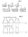
- a phase-controlled, regulated power supply circuit is shown to consist of a number of functional components 10, 20, 30, 40, 50, 60.
- a conventional ac power source 10 is connected to rectifier 20. Full wave rectified de signals are applied across lamp 30 and transistor switch 40.
- the operation of transistor switch 40 is controlled by a feedback loop consisting of photosensor 50 and comparator-amplifier 60.
- Photosensor 50 generates an output signal proportional to the intensity of light emanating from lamp 30.
- the signal is amplified and compared, in comparator-amplifier 60, with a fraction of the rectifier 20 output.
- the output of comparator-amplifier 60 is a voltage signal which changes at a rate which controls the operation of transistor switch 40, and, hence of lamp 30.
- FIG. 2 is a specific embodiment of the circuit shown in Figure 1.
- a ll5v 60 Hz line voltage from source 10 is applied to conventional dc bridge rectifier 20 which includes four diodes 20a, 20b, 20c and 20d, connected as shown.
- Rectifier 20 converts the applied ac power to full wave rectified dc power across output leads 22, 24.
- the output on lead 22 has a 120 cps ripple component which is filtered by a circuit comprising capacitor 26, zener diode 27 and resistor 28. This filtered de voltage is then used to provide power, along lead 25 to the amplifier circuits and a biasing signal to circuit 60, as will be seen.
- the full wave, rectified dc output on lead 22 is applied to a 100W, 100V tungsten lamp 30 in series with transistor switch 40 consisting of Darlington transistor 42 and resistors 44, 45.
- the function of transistor 43 is to provide an overcurrent shutdown of the output to protect transistor pair 42 during warmup of the lamp.
- Photosensor circuit 50 which monitors the light output of lamp 30, includes a photodiode 52, and operational amplifier 54. Photodiode 52 generates an output current proportional to the irradiance from lamp 30 impinging thereon. Capacitor 56 filters out any ripple components.
- Amplifier 54 provides a current-to-voltage conversion of the photodiode signal and its output signal V L is proportional to the input photodiode signal and the gain of the circuit (controlled by potentiometer 58).
- Voltage signal V L is applied to the positive input of operational amplifier 61 in amplifier-comparator circuit 60.
- the rectified, filtered output from lead 22 is applied to the negative input of amplifier 61 across a voltage divide comprising resistors 62, 63.
- Amplifier 61 output signal, V c is proportional to the input signal from amplifier 54 and the gain of the circuit as set by resistor 64. For the selected component values, amplifier 61 provides a non-inverted voltage output with a gain of approximately 10.
- the voltage output, V , of amplifier 61 is applied to the negative input of operational amplifier 65 across resistor 66. This input is compared with a fraction of the rectified line voltage on lead 22, applied to amplifier 65 across a voltage divider consisting of resistors 67, 68.
- the output V o of amplifier 65 is therefore proportional to the input signal from amplifier 61 and the gain as set by resistor 69.
- amplifier 65 provides a non-inverted voltage output V with a gain of approximately 11. This signal is applied to transistor switch circuit 40.
- the rate at which output V changes (along with the value of resistor 44 and the gain of transistor 42) affects the rate at which the lamp current changes.
- V 0 will go positive whenever the input to the positive terminal of amplifier 65 is sufficiently positive with respect to the input V c at the negative terminal.
- V will be a minimal value since current is not flowing through lamp 30 and photodiode 52 is not detecting any light output.
- V 0 will go positive at some point A on the full wave waveform at some time value k (t) after full power application. Since V goes positive, transistor 42 is biased into conduction and power is applied to lamp 30. Transistor 42 will continue to conduct until the bias voltage to amplifier 65 drops below the preset value at A', at which point transistor 42 is turned off.
- Lamp 30 has therefore been energized for some period t l and has produced a light component which is detected by photodiode 52.
- the amplified signal will be present as signal V c at the negative input of amplifier 65.
- Amplifier 65 will therefore not go positive until it sees a greater line voltage input B at the positive terminal.
- Transistor 42 will then be turned on and conduct during a shorter time period t 2 terminated at point B', where the line voltage drops below the value of V .
- the photosensor signal generates a signal proportional to the increased light output of lamp 30. It can then be appreciated that with the application of each successive line voltage waveform, up to the point where equilibrium conditions are achieved, V c will continue to increase causing V to go positive at greater values of the applied line voltage.
- Waveform C illustrates a typical waveform for normal lamp operating conditions for the circuit shown in Figure 2, and with a current gain of 200 for transistor 42, lamp current will increase from 0 to 1 ampere when the line voltage has a net change of approximately 10 volts.
- the time required for the line voltage to change by 10 volts depends on the shape of the line voltage waveform but at the steepest part, the time required for a 10 volt change is 165 ⁇ sec.
- FIGURE 2 COMPONENTS
- the circuit of Figure 2 has been modified by introducing an additional amplifier in the trigger circuit and using the Darlington transistor as the output.
- the circuit operates in the same manner as described above producing voltage V at the output of comparator-amplifier 65.
- This drive voltage is divided down by resistors 70 and 71 to provide a low-level, control voltage to amplifier 72.
- Amplifier 72 drives Darlington transistor pair 73 via resistor 74 so that the current from lamp 30 causes a voltage drop across resistor 75 equal to the control voltage.
- the voltage gain of amplifier 72 as set by resistors 76, 77, equals 150, so that sufficient base-drive voltage will always be present to operate transistor pair 73, regardless of its current gain.
- Transistor 78 serves the same function as transistor 43 in Figure 2. It is therefore seen that, since the output signal V is an approximate representative of the desired output current, the introduction of high gain closed loop transconductance (voltage to current converter) amplifier 72 removes the undesirable effects of current gain changes in the Darlington transistor.
- FIGURE 4 (Switch 40) Components
- the lamp has been phased into a normal operating mode by controlling lamp turn-on and turn-off via a transistor switching circuit thereby reducing the electromagnetic affects associated with the more rapid SCR turn-on techniques.
- the principles of the present invention are applicable to the application of power to other types of loads such as radiant heaters, for example, of the type used to fuse xerographic images on a recording sheet.
- a sensing element which detects radiant heat emanating from the fuser could be used in place of the photodiode.
Landscapes
- Circuit Arrangement For Electric Light Sources In General (AREA)
- Control Of Electrical Variables (AREA)
- Continuous-Control Power Sources That Use Transistors (AREA)
Applications Claiming Priority (2)
| Application Number | Priority Date | Filing Date | Title |
|---|---|---|---|
| US285236 | 1981-07-20 | ||
| US06/285,236 US4423478A (en) | 1981-07-20 | 1981-07-20 | Phase controlled regulated power supply |
Publications (2)
| Publication Number | Publication Date |
|---|---|
| EP0070664A1 true EP0070664A1 (de) | 1983-01-26 |
| EP0070664B1 EP0070664B1 (de) | 1986-10-08 |
Family
ID=23093373
Family Applications (1)
| Application Number | Title | Priority Date | Filing Date |
|---|---|---|---|
| EP82303638A Expired EP0070664B1 (de) | 1981-07-20 | 1982-07-12 | Mittels Phasenkontrolle gesteuerte Speiseschaltung |
Country Status (5)
| Country | Link |
|---|---|
| US (1) | US4423478A (de) |
| EP (1) | EP0070664B1 (de) |
| JP (1) | JPS5818719A (de) |
| CA (1) | CA1195374A (de) |
| DE (1) | DE3273706D1 (de) |
Cited By (4)
| Publication number | Priority date | Publication date | Assignee | Title |
|---|---|---|---|---|
| DE3418857A1 (de) * | 1983-05-21 | 1984-12-06 | Hayashibara, Ken, Okayama | Stromversorgungsanordnung fuer eine gluehlampe hoher leuchtkraft |
| DE3339522A1 (de) * | 1983-11-02 | 1985-05-09 | Faseroptik Henning GmbH & Co, 8501 Allersberg | Stabilisierte kaltlichtquelle |
| US4777409A (en) * | 1984-03-23 | 1988-10-11 | Tracy Stanley J | Fluorescent lamp energizing circuit |
| GB2244394A (en) * | 1990-02-07 | 1991-11-27 | Harold Aspden | Electric surface heating |
Families Citing this family (20)
| Publication number | Priority date | Publication date | Assignee | Title |
|---|---|---|---|---|
| US4823069A (en) * | 1984-08-15 | 1989-04-18 | Michael Callahan | Light dimmer for distributed use employing inductorless controlled transition phase control power stage |
| US5629607A (en) * | 1984-08-15 | 1997-05-13 | Callahan; Michael | Initializing controlled transition light dimmers |
| US5319301A (en) * | 1984-08-15 | 1994-06-07 | Michael Callahan | Inductorless controlled transition and other light dimmers |
| US4633161A (en) * | 1984-08-15 | 1986-12-30 | Michael Callahan | Improved inductorless phase control dimmer power stage with semiconductor controlled voltage rise time |
| US5225765A (en) * | 1984-08-15 | 1993-07-06 | Michael Callahan | Inductorless controlled transition and other light dimmers |
| DE3815604A1 (de) | 1988-05-06 | 1989-11-23 | Texas Instruments Deutschland | Treiberschaltung |
| US4983884A (en) * | 1989-08-29 | 1991-01-08 | Amp Incorporated | Constant intensity light source for fiber optic testing |
| CN1033254C (zh) * | 1991-07-04 | 1996-11-06 | 蒋子刚 | 双渐变电子开关 |
| JPH05160691A (ja) * | 1991-12-04 | 1993-06-25 | Nikon Corp | 2値化しきい値設定回路 |
| JPH05343185A (ja) * | 1992-06-05 | 1993-12-24 | Kagatsuu Kk | 照明灯の点灯判別装置 |
| US5576614A (en) * | 1994-05-27 | 1996-11-19 | Xerox Corporation | Circuit for supplying constant voltage to a lamp from an AC input |
| US5661645A (en) | 1996-06-27 | 1997-08-26 | Hochstein; Peter A. | Power supply for light emitting diode array |
| DE69803064T2 (de) * | 1998-09-01 | 2003-01-23 | Mass Technology (H.K.) Ltd., Kowloon | Stromversorgung für Brom-Tungsten Wendellampe |
| US6208122B1 (en) | 1999-09-28 | 2001-03-27 | Triatek, Inc. | High frequency pulse width modulation of AC current for control of lighting load power |
| US6486499B1 (en) | 1999-12-22 | 2002-11-26 | Lumileds Lighting U.S., Llc | III-nitride light-emitting device with increased light generating capability |
| US6514782B1 (en) | 1999-12-22 | 2003-02-04 | Lumileds Lighting, U.S., Llc | Method of making a III-nitride light-emitting device with increased light generating capability |
| US6885035B2 (en) | 1999-12-22 | 2005-04-26 | Lumileds Lighting U.S., Llc | Multi-chip semiconductor LED assembly |
| US6573537B1 (en) | 1999-12-22 | 2003-06-03 | Lumileds Lighting, U.S., Llc | Highly reflective ohmic contacts to III-nitride flip-chip LEDs |
| US6903376B2 (en) * | 1999-12-22 | 2005-06-07 | Lumileds Lighting U.S., Llc | Selective placement of quantum wells in flipchip light emitting diodes for improved light extraction |
| US8636885B2 (en) * | 2010-02-26 | 2014-01-28 | Dionex Corporation | Analytic device with photovoltaic power source |
Citations (1)
| Publication number | Priority date | Publication date | Assignee | Title |
|---|---|---|---|---|
| US4101808A (en) * | 1975-09-30 | 1978-07-18 | Bell & Howell Company | Lamp control circuit |
Family Cites Families (8)
| Publication number | Priority date | Publication date | Assignee | Title |
|---|---|---|---|---|
| GB994425A (en) * | 1961-03-15 | 1965-06-10 | Int Computers & Tabulators Ltd | Improvements in or relating to current regulating circuits |
| US3456155A (en) * | 1965-04-30 | 1969-07-15 | Advance Data Systems Corp | Photosensitive circuit for controlling the intensity of a lamp |
| US3952242A (en) * | 1969-04-11 | 1976-04-20 | Ricoh Co., Ltd. | Automatic voltage regulator with optical feedback |
| US3670202A (en) * | 1970-07-31 | 1972-06-13 | Nasa | Ultrastable calibrated light source |
| JPS51122745A (en) * | 1975-04-21 | 1976-10-27 | Toshiba Corp | Dc constant-voltage power source circuit |
| US4042856A (en) * | 1975-10-28 | 1977-08-16 | General Electric Company | Chopper ballast for gaseous discharge lamps with auxiliary capacitor energy storage |
| JPS5520586A (en) * | 1978-07-31 | 1980-02-14 | Sharp Corp | Power control unit |
| JPS5566274A (en) * | 1978-11-13 | 1980-05-19 | Fuji Electric Co Ltd | Chopper-control apparatus |
-
1981
- 1981-07-20 US US06/285,236 patent/US4423478A/en not_active Expired - Fee Related
-
1982
- 1982-05-18 CA CA000403207A patent/CA1195374A/en not_active Expired
- 1982-07-08 JP JP57119156A patent/JPS5818719A/ja active Pending
- 1982-07-12 DE DE8282303638T patent/DE3273706D1/de not_active Expired
- 1982-07-12 EP EP82303638A patent/EP0070664B1/de not_active Expired
Patent Citations (1)
| Publication number | Priority date | Publication date | Assignee | Title |
|---|---|---|---|---|
| US4101808A (en) * | 1975-09-30 | 1978-07-18 | Bell & Howell Company | Lamp control circuit |
Non-Patent Citations (1)
| Title |
|---|
| XEROX DISCLOSURE JOURNAL, vol. 3, no. 6, November/December 1978, page 453, Stamford, (USA) * |
Cited By (4)
| Publication number | Priority date | Publication date | Assignee | Title |
|---|---|---|---|---|
| DE3418857A1 (de) * | 1983-05-21 | 1984-12-06 | Hayashibara, Ken, Okayama | Stromversorgungsanordnung fuer eine gluehlampe hoher leuchtkraft |
| DE3339522A1 (de) * | 1983-11-02 | 1985-05-09 | Faseroptik Henning GmbH & Co, 8501 Allersberg | Stabilisierte kaltlichtquelle |
| US4777409A (en) * | 1984-03-23 | 1988-10-11 | Tracy Stanley J | Fluorescent lamp energizing circuit |
| GB2244394A (en) * | 1990-02-07 | 1991-11-27 | Harold Aspden | Electric surface heating |
Also Published As
| Publication number | Publication date |
|---|---|
| DE3273706D1 (en) | 1986-11-13 |
| US4423478A (en) | 1983-12-27 |
| CA1195374A (en) | 1985-10-15 |
| EP0070664B1 (de) | 1986-10-08 |
| JPS5818719A (ja) | 1983-02-03 |
Similar Documents
| Publication | Publication Date | Title |
|---|---|---|
| US4423478A (en) | Phase controlled regulated power supply | |
| US4809150A (en) | DC to DC converter with feed forward and feed back regulation | |
| US4224563A (en) | Regulator circuit for photographic illumination | |
| US5754419A (en) | Surge and overcurrent limiting circuit for power converters | |
| US4327309A (en) | Fluorescent lamp power supply with low voltage lamp polarity reversal | |
| US6359266B2 (en) | Flicker free fuser control | |
| KR960033174A (ko) | 원격 램프 부하 제어 방법 | |
| GB2152772A (en) | Electrical power control system | |
| EP0556116B1 (de) | Schaltung zur Leistungssteuerung einer Kochstelle mit Induktionserwärmung | |
| US5698908A (en) | Buffered DC power supply system | |
| US4398132A (en) | Electron beam current stabilizing device | |
| DE4125229C2 (de) | Stromstoßunterdrückungsschaltung für eine Induktionskochvorrichtung | |
| US5490450A (en) | Inverter cooker with a high voltage/low voltage separating device | |
| EP0268487B1 (de) | Lichteinstellungseinrichtung | |
| US4484256A (en) | Constant current density high voltage power supply | |
| GB2173928A (en) | Current regulation in an inductive load | |
| CA2051363C (en) | Optical fiber fusion splicer | |
| JPS58112478A (ja) | インバ−タの制御回路 | |
| US5196832A (en) | Electric power system with line failure detection | |
| US4766363A (en) | Voltage limiting control system for heat emitting loads | |
| US5703790A (en) | Series connection of multiple digital devices to a single power source | |
| JPH0785648B2 (ja) | スイッチングレギュレータ電源回路 | |
| US3210647A (en) | Current regulating circuits employing light sensitive means and pulse width modulation control | |
| JPH1014112A5 (de) | ||
| US4194160A (en) | Noninteractive heater power supply |
Legal Events
| Date | Code | Title | Description |
|---|---|---|---|
| PUAI | Public reference made under article 153(3) epc to a published international application that has entered the european phase |
Free format text: ORIGINAL CODE: 0009012 |
|
| AK | Designated contracting states |
Designated state(s): DE GB |
|
| 17P | Request for examination filed |
Effective date: 19830725 |
|
| GRAA | (expected) grant |
Free format text: ORIGINAL CODE: 0009210 |
|
| AK | Designated contracting states |
Kind code of ref document: B1 Designated state(s): DE GB |
|
| REF | Corresponds to: |
Ref document number: 3273706 Country of ref document: DE Date of ref document: 19861113 |
|
| PLBE | No opposition filed within time limit |
Free format text: ORIGINAL CODE: 0009261 |
|
| STAA | Information on the status of an ep patent application or granted ep patent |
Free format text: STATUS: NO OPPOSITION FILED WITHIN TIME LIMIT |
|
| 26N | No opposition filed | ||
| PGFP | Annual fee paid to national office [announced via postgrant information from national office to epo] |
Ref country code: GB Payment date: 19900522 Year of fee payment: 9 |
|
| PGFP | Annual fee paid to national office [announced via postgrant information from national office to epo] |
Ref country code: DE Payment date: 19900731 Year of fee payment: 9 |
|
| PG25 | Lapsed in a contracting state [announced via postgrant information from national office to epo] |
Ref country code: GB Effective date: 19910712 |
|
| GBPC | Gb: european patent ceased through non-payment of renewal fee | ||
| PG25 | Lapsed in a contracting state [announced via postgrant information from national office to epo] |
Ref country code: DE Effective date: 19920401 |