EP0070666A2 - Système optique d'inspection - Google Patents
Système optique d'inspection Download PDFInfo
- Publication number
- EP0070666A2 EP0070666A2 EP82303647A EP82303647A EP0070666A2 EP 0070666 A2 EP0070666 A2 EP 0070666A2 EP 82303647 A EP82303647 A EP 82303647A EP 82303647 A EP82303647 A EP 82303647A EP 0070666 A2 EP0070666 A2 EP 0070666A2
- Authority
- EP
- European Patent Office
- Prior art keywords
- output
- workpiece
- camera
- fed
- scan
- Prior art date
- Legal status (The legal status is an assumption and is not a legal conclusion. Google has not performed a legal analysis and makes no representation as to the accuracy of the status listed.)
- Withdrawn
Links
Images







Classifications
-
- G—PHYSICS
- G01—MEASURING; TESTING
- G01B—MEASURING LENGTH, THICKNESS OR SIMILAR LINEAR DIMENSIONS; MEASURING ANGLES; MEASURING AREAS; MEASURING IRREGULARITIES OF SURFACES OR CONTOURS
- G01B11/00—Measuring arrangements characterised by the use of optical techniques
- G01B11/24—Measuring arrangements characterised by the use of optical techniques for measuring contours or curvatures
-
- B—PERFORMING OPERATIONS; TRANSPORTING
- B07—SEPARATING SOLIDS FROM SOLIDS; SORTING
- B07C—POSTAL SORTING; SORTING INDIVIDUAL ARTICLES, OR BULK MATERIAL FIT TO BE SORTED PIECE-MEAL, e.g. BY PICKING
- B07C5/00—Sorting according to a characteristic or feature of the articles or material being sorted, e.g. by control effected by devices which detect or measure such characteristic or feature; Sorting by manually actuated devices, e.g. switches
- B07C5/04—Sorting according to size
- B07C5/10—Sorting according to size measured by light-responsive means
-
- G—PHYSICS
- G01—MEASURING; TESTING
- G01B—MEASURING LENGTH, THICKNESS OR SIMILAR LINEAR DIMENSIONS; MEASURING ANGLES; MEASURING AREAS; MEASURING IRREGULARITIES OF SURFACES OR CONTOURS
- G01B11/00—Measuring arrangements characterised by the use of optical techniques
- G01B11/02—Measuring arrangements characterised by the use of optical techniques for measuring length, width or thickness
- G01B11/022—Measuring arrangements characterised by the use of optical techniques for measuring length, width or thickness by means of tv-camera scanning
Definitions
- One way of achieving this is to inspect workpieces using a video camera and then to analyse the video signals output from the video camera to derive information with regard to the workpiece.
- an optical inspection system for the inspection of circular workpieces includes an electronic camera having an optical system for focusing an image of a circular workpiece on its electronically active image receiving surface, means to move circular workpieces into a predetermined position in the field of view of the optical system of the camera, means for scanning the image receiving surface in directions extending substantially radially across the image receiving surface to produce an output signal, and a signal analyser arranged to monitor the output signal corresponding to each radial scan to detect the presence of any irregularity in the workpiece.
- the video output signal corresponding to each radial scan of a circular workpiece is substantially the same. This means that these output signals can be analysed much more readily to analyse the signals to monitor the radius or the circularity of the workpiece, or monitor the presence of any other feature that occurs, or should occur, at a predetermined distance along each radial scan.
- the signal analyser may be arranged to compare the output signals corresponding to each scan with succeeding scans to detect any changes or differences between them.
- the signals corresponding to each scan are monitored to determine the presence at the required position along each scan of each element of the workpiece and to determine the absence of any unexpected elements along each scan.
- the output signal corresponding to each scan may be compared with predetermined data corresponding to the output signal produced by the system when it inspects a perfect workpiece but preferably the output signal correspading to each scan is monitored over different timing windows to detect the presence or absence of an event in each timing window.
- the optical inspection system in accordance with this invention also includes an illuminating system capable of illuminating the workpiece for only a short period of time.
- an illuminating system capable of illuminating the workpiece for only a short period of time.
- the system includes position sensing means to sense the position of the means to move the workpiece or the position of a workpiece at a predetermined position with respect to the camera to provide a triggering signal as the workpiece is moved into the field of view of the optical system of the camera.
- the triggering signal preferably triggers the operation of the illumination source and also triggers the scanning of the electronically active image receiving surface of the camera.
- the latent electrical image formed on the image receiving surface of the camera is scanned from its centre and in the radially outwards direction.
- the electraically active image receiving surface of the electronic camera is a standard vidicon tube having standard X and Y axis deflection coils.
- the means for scanning the image receiving surface preferably include means to generate two signals having a sinusoidal waveform but being 90° out of phase and two ramp generators fed with the two signals having a sinusoidal waveform so that the output of the ramp generators are two saw tooth waveforms whose amplitudes are modulated by sine and cosine waveforms.
- the output signals from the ramp generators are fed to the X and Y axis deflection coils of the vidicon tube and these result in the electron beam of the vidicon tube scanning the target of the vidicon tube in a series of substantially radial outward sweeps starting at the centre and precessing around the target.
- a conventional vidicon tube it is possible to use other forms of video camera and it would also be possible to use a camera including a photodiode array or matrix or a charged coupled device array or matrix provided that the photodiode or charge coupled devices have a radial distribution.
- This invention has a particular application as an optical inspection system for inspecting a crown cap for a bottle.
- a sealing material is moulded onto the inside of a crown cap for a bottle in the form of an annular rib which, in use, seals against the open end of the neck of the bottle and a thinner layer completely filling the centre of the annular rib to provide a surface coating over the inside of the crown cap.
- the inspection system in accordance with this invention is particularly good at inspecting such objects because it can readily monitor the radial width of the annular seal portion and also monitor the continuity of the surface coating over the inside of the cap.
- the apparatus in accordance with this invention also checks the formation of the flutes in the side wall of the crown cap.
- the crown-type bottle cap comprises a metal cap 1 with a crimped and fluted side wall 2.
- the closed end wall 3 of the cap has a sealing compound moulded onto it in the form of an annular upstanding rib 4 which, in use, seals against the open end of the neck of the bottle and a thinner coating of the sealing compound 5 filling the central portion of the annular rib 4 and covering the closed end wall 3 of the cap 1.
- the portion 5 provides an inert coating to cover the inside of the cap 1.
- the central panel 5 of the sealing compound is uniform and free from any unwanted inclusions or breaks; the second is that the upstanding annular rib 4 is of sufficient width to form an effective seal with the open end of a neck of a bottle; and, the third is that the side wall 2 of the cap is crimped and fluted.
- the crown-type bottle cap is viewed by a video camera and the image of the bottle cap formed in the video camera is scanned in substantially radial directions and this is illustrated schematically in Figure 3.
- a substantially uniform video signal is obtained from each scan if the cap is correctly formed.
- the system is arranged so that the image of the cap is scanned radially from its centre 256 times with the radius of scanning moving around a complete circle, but in Figure 3 only seven scanning lines are indicated.
- the video signals obtained are then analysed to determine if the cap is correctly formed and, if irregularities are detected, the cap is rejected.
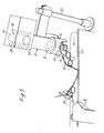
- the optical inspection system comprises, as shown in Figure 4, a video camera 6, electronic circuits 7, required to power the camera including those that produce the radial scan, a pulsed light source 8, an electronic light control circuit 9 to drive the light source 8, a position detector 10, synchronising electronics 11, signal analysis electronics 12, a reject driver circuit 13, and a reject station 14.
- Bottle caps 1 are fed from a seal moulding machine into recesses 15 in a rotating star wheel 16.
- a belt conveyor 17 passes beneath the periphery of the star wheel 16 and the caps 1 are taken away from the recesses 15 in the star wheel l6 by the belt conveyor 17.
- the belt conveyor 17 feeds a downstream collection plant.
- a reject chute 18 is located at the side and away from the belt conveyor 17 and leads to a reject bin (not shown).
- a solenoid operated air valve 19 is located above the belt conveyor 17 and includes a nozzle 20 to direct a blast of compressed air against any faulty crown 1 on the belt conveyor 17 to push it off the belt 17 and into the reject chute 18.
- the video camera 6 including a lens system 21, a vidicon tube 22 having a target 23 and two pairs of deflection coils 24 arranged at right angles to one another, only one pair of which is shown, is mounted on a support column 25 so that the aperture of its lens system 21 is directly above the path of the centre of the caps 1.
- the light source 8 surrounds the end of the lens system 21 of the camera and is interposed between this and the star wheel 16.
- a photoemitter/photodetector pair 10 is located beneath the star wheel l6 so that the beam of light passing from the photoemitter to the photodetector is interrupted by the passage of a series of pins (not shown) depending from the star wheel l6 in angular positions corresponding to those of the receiver 15.
- the structure of the video camera 6 is entirely conventional and the lens system 21 causes an image of the caps 1 to be focused on the sensitive face of the silicon target.23.
- a conventional focusing coil, its associated control circuitry, and a video amplifier are also provided in the video camera 6 and these are also entirely conventional in construction.
- the use of silicon as the target material of the vidicon tube is preferred in this system since it offers a low value of charge retention after scanning and this allows a high throughput rate of caps 1.
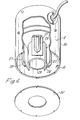
- the pulsed light source 7 comprises three high pulse rate flash tubes 27 with local diffusing elements 28 placed symmetrically around a cylindrical diffuser 29.
- the cylindrical diffuser 29 surrounds the lens system 21 of the video camera 6 so that the pulsed lighting system 8 is concentric with the video camera 6.
- the flash tubes 27 and diffusers 28 and 29 are mounted inside a cylindrical housing 30 having a high reflectivity inner surface 31.
- the lower end of the light source is covered by an annular end cover 32.
- the light source 7 is arranged to provide lighting which is uniform around the cap 1 but which is steeply inclined to the surface of the end wall 3 of the cap 1.
- the operation of the flash tubes 27 is triggered by the pins (not shown) passing through the light path between the photodetector and photoemitter pair 10 as the next cap 1 approaches the optical system 21 of the camera 6 so that the flash tubes illuminate the cap 1 when it is directly beneath the video camera 6.
- the pulsed illumination provided by the light source 8 thus, effectively, freezes the movement of the caps 1.
- the flash tubes 27 are operated by a capacitive energy storage-discharge system shown in Figure 7.
- Two 150 volt zener diodes ZD1 and ZD2 control the voltage via a transistor TRl that is supplied to charging capacitors Cl, C2 and C3 connected in parallel across the flash tubes 27.
- a flash trigger pulse produced by the synchronising electronics 11 in response to the output from the photoemitter/photodetector pair 10 is applied to_ the gate of a thyristor SCR1 via the terminal Tl.
- a high voltage is generated via the transformer TF1 and applied to the firing electrodes of the flash tubes 27.
- the deflection coils 24 which would normally deflect the scanning beam in the X axis direction have less turns in them than the deflection coils 24 that would normally deflect the scanning beam in the Y axis direction.
- a 50Hz sine wave is fed from the synchronising electronics 11 via terminal T2 and a radius reset pulse from the synchronising electroincs 11 via terminal T3.
- the 50Hz sine wave from terminal T2 is amplified by amplifier Al and then fed to an integrator consisting of operational amplifier A2 and resistor and capacitor network Rl, C4.
- the output from amplifier Al is also fed to amplifier A3 with resistor R2 and capacitor C5 arranged to produce a phase shift of 90°.
- the output of the amplifier A3 is fed to a further amplifier A4 including an integrating network formed by a resistor R3 and capacitor C6. The output from amplifier A4 is thus 90° out of phase with the output from amplifier A2.
- Capacitors C4 and C6 have connected in parallel with them separate stages of an analogue switch ICla and IClb respectively. These stages of the analogue switch IC1 are controlled by the radius reset pulse supplied to terminal T3 so that, upon receipt of the radius reset pulse the analogue switch IC1 discharges the capacitors C4 and C6.
- a feedback signal developed across resistors R4 and R5 are fed back to the amplifiers A5 and A6.
- the push-pull scan coil drive amplifier connected to the y axis deflection coil 24 operates with a plus and minus 24 volt supply whereas the output push-pull drive amplifier for the X axis deflection coil 24 operates with a plus and minus 6 volt power supply.
- the higher voltage output is provided for the Y axis deflection coil than for the X axis deflection coil to take account of the difference in their number of turns.
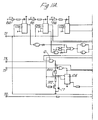
- An integrated circuit sine wave oscillator IC2 having a frequency adjusting potentiometer RV1 feeds a 50Hz sine wave through a buffer amplifier A7 to the terminal T2 from which, as already described, it is fed to the scan coil driver illustrated in Figure 8.
- the 50Hz sine wave is also fed to a zero crossing detector in the form of a Schmitt trigger circuit including an amplifier A8.
- the square wave output from the Schmitt trigger circuit is differentiated by resistor capacitor network R10, Cll to produce a short pulse at the output of the second stage of a double inverter IC3. This pulse occurs on the negative transition through zero of the 50Hz sine wave and is used to produce a start of the modulated scan pulse (S.M.S).
- the SMS pulse output from IC3 is fed to a CMOS integrated circuit phase locked loop IC4.
- the oscillator output from the phase locked loop IC4 is fed to the clock input of the monostable multivibrator IC5.
- the Q output of the dual monostable multivibrator IC5 is fed to a divide by 256 counter IC6, formed by a dual four bit binary counters IC6a and IC6b connected one after the other.
- the output from the divide by 256 counter IC 6 is then returned to the phase locked loop IC4 where it is compared with the SMS pulse by the phase comparator of the phase locked loop to complete the phase locked loop.
- the oscillator of the phase locked loop provides 256 output pulses in between each input SMS pulse i.e.
- the Q output of the monostable multivibrator IC5 which forms the radius reset pulse is fed to the terminal T3 and from there to the scanning coil driver circuit shown in Figure 8.
- the pulse width of the radius reset pulse is set by adjustment of the variable resistor RV2 to a pulse width of 10 ⁇ s .
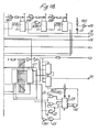
- the SMS pulses are also fed from the output of IC3 to a start up delay circuit DC not shown in detail.
- the start up delay circuit DC at the conclusion of the start up delay circuit sends a constant signal to terminal T4.
- the beam of light passing between the photodetector/photoemitter pair 10 is interrupted causing a falling edge on the output of the photodetector.
- This falling edge is fed to the clock input terminal of a first half IC7a of a dual monostable multivibrator IC7.
- the pulse duration of the monostable multivibrator IC7 is set by the variable resistance RV3 and, on relaxing the first half IC7 a of the dual monostable multivibrator IC7 initiates the second half IC7b to produce a '1" on the D input of the first part of a dual D flip flop IC8.
- the radius reset pulse is connected to the clock input of the flip flop IC8a s:o that upon receipt of the next radius reset pulse, the Q output of the flip flop IC8a goes positive providing a flash trigger pulse on output terminal Tl which is connected to the pulsed light source and capacitive energy storage-discharge system shown in Figure 7, to cause a flash of light to be emitted by the flash tubes 27.
- the next radius reset pulse causes the resetting of the flip flop IC8a and thus the flash trigger pulse is one scan line in duration.
- a start of scan pulse (SOS) is generated on the Q output of the second half IC8b of the dual D flip flop IC8. This SOS pulse is used to set the Q terminal of the flip flop IC9 to "1".
- the oscillator output signal from the phase locked loop IC4 is also fed to a second dual four bit binary counter IC 10 which is also arranged to count 256 bits.
- the output from the counter IC10 is fed to the reset input of the flip flop IC9 to reset the flip flop IC9 after 256 radius reset pulses have been counted by the counter IC10.
- the signal output by the Q output of flip flop IC9 remains at "1"for one complete cycle of the sine wave oscillator IC2 and is called a scan duration pulse SD.
- the scan duration pulse is fed to output terminal T5.
- the signal analysis circuit monitors the presence or absence of defects in the cap with reference to whether particular video events are present or absent during particular timing windows.
- the means to generate the timing windows are shown in Figure 11 and comprise a series of monostable multivibrators.
- a first half IClla of a dual monostable multivibrator IC11 is used to determine the fly back duration period which is set by variable potentiometer RV4.
- the radius reset pulse from the terminal T3 is used to clock the multivibrator IClla and the output from the Q terminal of the multivibrator IClla produces a fly-back blank pulse (F.B). This pulse is used to suppress the output from the vidicon tube during flyback of the scanning beam.
- F.B fly-back blank pulse
- the other half ICllb of the dual monostable multivibrator IC11 is arranged to produce the flute display window (FDW).
- This monostable multivibrator is also clocked from the radius reset pulse applied to terminal T3 and has connected to it variable potentiometer RV5 which enables the width of the flute display window to be varied.
- the signal to form the flute display window is taken from the Q output of the monostable multivibrator ICllb to terminal T6.
- the first part of a further dual monostable multivibrator IC12a produces a centre to seal pulse (CSP).
- the time period of this multivibrator is varied by the variable potentiometer RV6 and the clock input of this multivibrator again has the radius reset pulse from terminal T3 applied to it.
- the Q output from the multivibrator IC12a is fed to an output terminal T7.
- the soutput is fed to the other part of the monostable multivibrator ICl2b.
- the time period of the monostable multivibrator IC12b is set by the variable potentiometer RV7 and this monostable multivibrator determines the duration of the seal window.
- the monostable multivibrator lCl2b is clocked by the Q pulses from the monostable multivibrator IC12a and the Q output from the monostable multivibrator ICl2b is fed to an output terminal T8.
- the output from the Q output of the monostable multivibrator IC12b is fed to the clock input of a further monostable multivibrator IC13a having a variable potentiometer RV8 arranged to control its period.
- This monostable multivibrator IC13a sets the seal to flute time (SFT) and the output from the Q terminal of this monostable multivibrator is fed to the clock input terminal of a monostable multivibrator ICl3b, which sets the flute glimpse time pulses (SCG).
- SFT seal to flute time
- SCG flute glimpse time pulses
- the period of the-monostable multivibrator IC13b is set by variable potentiometer RV9.
- Figure 11 also shows the flute counting and detection circuitry.
- Flute detection pulses are received via terminal T9 and these are gated, together with the flute glimpse time pulses taken from the Q output of monostable multivibrator IC13b in an AND gate Gl.
- An output from AND gate Gl which represents the presence of a flute during the flute glimpse time window charges up capacitor C7 via variable potentiometer RV10.
- the rising edge of the output pulse from the Q output of the monostable multivibrator IC13b clocks the level on capacitor C7 into the D input of a D flip flop IC14 and this charges capacitor C7 via transistor TR2 and resistor R6.
- IC17 stores the condition of centre panel, seal and flute fault detection circuits during each radial scan.
- the centre panel and seal faults are input via terminals Tll and T12, respectively.
- the content of the memory IC17 is fed to fault counters to be described subsequently with reference to Figure 12 during the time period when the target 23 of the vidicon tube 21 is cleared.
- the signal analysis circuitry receives a balanced video signal via input terminals T13 and Tl4 which are fed to a differential amplifier A8.
- the resulting video signal is then further amplified in amplifier A9.
- This DC level resetting circuit ensures that the videosignal fed to the analysis circuit is unaffected by changes in the DC signal level from the video camera 6.
- the output from the amplifier A9 is fed to a peak detector including an amplifier A10 which holds the maximum video signal level generated during each radial scan
- the output of the amplifier A10 is inverted by inverting amplifier A21 and via two further amplifiers All and Al2 to the non-inverting input of a voltage comparator formed by differential amplifier A13.
- the level of the signal applied to the non-inverting input of differential amplifier A13 can be varied by adjustment of the variable potentiometer RV11.
- the video signal output from the differential amplifier A8 is differentiated by a resistor capacitor network R7C9 and applied to the inverting input of differential amplifier A13.
- the sensitivity of the centre panel defect detection circuit can not only be varied by adjusting the variable potentiometer RV11 but also the gain of the amplifier A14 forming part of the differentiator C9R7 can be varied by adjustment of the variable potentiometer RVl2.
- a seal fault is detected in one of two different ways. Firstly, the peak video signal output by amplifier A9 is compared with a DC reference voltage determined by resistors R9 and R10 and compared with one another in differential amplifier A15. Seal window timing pulses are fed via terminal T8 to a seal fault latch formed by dual D flip flops IC19a and IC19b. If the output of differential amplifier A15 is low this forces a low level into the D input of seal fault latch ICl9b to signify a seal fault. The other way in which a missing seal is detected is by the output from amplifier A9 being fed to a non-inverting integrator system including resistor Rll capacitor C10 and amplifier Al6 until the end of the centre to seal window pulse.
- the output from amplifier Al6 is fed to the inverting input of differential amplifier A17 whilst the peak video signal is fed to the non-inverting input of differential amplifier A17.
- the seal does not exist the output of differential amplifier A17 will stay low during the seal window and this also puts a low level on the D input of flip flop IC19b, the seal fault latch. If the seal is present but includes some mark such as an unwanted inclusion the differentiated peak video signal value will exceed the non-differentiated value.
- inverter A21 is fed via variable potentiometer RV13 to the non-inverting input of a differential amplifier A18 whilst the output from the differentiator including the capacitor C9 resistor C7 and amplifier A14 is fed to the inverting input of the differential amplifier A18.
- the output from the amplifier A18 goes high and this output is gated via AND gate G7 with the seal window pulse applied on terminal T8.
- the output of AND gate G7 is fed to the seal fault latch formed by the D flip flop IC19b and output from AND gate G7 resets the seal fault latch ICl9b to signify a seal fault.
- the peak video signal output from amplifier A10 is fed via a variable potential divider RVl4 to the non-inverting input of amplifier A19.
- the output from amplifier A19 is fed to the inverting input of a differential amplifier A20 and the video signal from amplifier A9 is fed to the non-inverting input of differential amplifier A20.
- the video signal is compared to a proportion as set by potential divider RVl4 of the peak video signal for that line. If a flute is present, the video signal is greater than the peak value and accordingly the output from differential amplifier A20 is high.
- differential amplifier A20 The output of differential amplifier A20 is forced to zero except from the middle of the seal window onwards as defined by inverter INV4 and OR gate G8 which is fed with a centre seal pulse from terminal T7.
- the output from differential amplifier A20 is fed to terminal T9 and to the flute counting arrangement already described with reference to Figure 11.
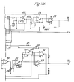
- FIG. 13 The part of the signal analysis circuit that counts the occurrence of fault signals and controls the operation of the reject drive 13 is illustrated in Figure 13.
- a centre panel fault occurs a high signal is applied via terminal Tll to the input of AND gate G9.
- Another input to AND gate G9 comes from terminal T7 and is the centre panel to seal time window.
- an output is provided from AND gate G9 to the set terminal of an RS flip flop IC20 which in turn takes the Q output of the RS flip flop IC20 high.
- the Q output of IC20 resets one part IC2la and increments the other part IC2lb of a dual four bit binary counter IC21.
- the Q output from IC20 is fed to the counter IC21 via an AND gate G10 in which it is gated with an end of seal window pulse applied to terminal T15.
- the end of seal window pulse applied to terminal T15 is obtained by differentiating the seal window pulse appearing on terminal T8 with capacitor C 11 and inverter INV 5 shown on Figure llb.
- the outputs of the counter IC21b are fed to a selector switch SW1 and when the count incremented on counter IC2lb exceeds that set by selector switch SW1 a signal is sent to the set input of RS flip flop IC22 which in turn, via a three-state latch IC32 lights a light emitting diode LED1 to indicate the presence of a centre panel fault and also provides a faulty crown indication on terminal Tl6 via OR gate Gll. If two consecutive good scans are received by the counter IC2la before the count in IC21b reaches the value set by selector switch SW1 then counter IC21a resets counter IC2lb so preventing a centre panel fault indication and corresponding faulty cap indication being given on terminal T16.
- D flip flop IC23 During each radial scan the part of the scan corresponding to the very middle of the centre panel section is blanked out using D flip flop IC23.
- This flip flop is clocked by radius reset pulses from terminal T3 and its delay period is set by variable potential divider RVl5.
- the output from the D flip flop IC23 is fed to the reset input of RS flip flop IC20.
- the mould number of the mould forming the centre panel 3 and seal 4 on each cap 1 is moulded into the very centre of the central panel 3 and the presence of this mould number can appear to the optical inspection system as a fault and this can be overcome by varying the setting of variable potential divider RV15 to control the duration of the delay introduced by the flip flop IC23.
- an input signal is provided via terminal T12 onto the D input of D flip flop IC24.
- the end of seal window pulse from terminal T15 is applied to the clock input of D flip flop IC24 so that the seal fault signal is clocked through the flip flop IC24 and the resultant low level on the Q output of D flip flop IC24 is applied to the reset input of a good seal counter formed by a first part IC25a of a dual four bit binary counter and to increment the other part IC25b of the dual four bit binary counter IC25 which forms a bad seal counter.
- the Q output from D flip flop IC24 is fed to the reset input counter IC25a through an inverter INV6 and an AND gate G12 where it is clocked with an end of seal window pulse from terminal T15. If no seal fault is present at terminal T12 the Q output is high and this is applied via AND gate G13. though which it is clocked by an end of seal window pulse from terminal T15,.into the clock input of the good seal counter IC25a. If more faulty seal signals are detected during scanning of the same cap the good seal counter is reset and the bad seal counter incremented further.
- Selector switch SW2 is connected to the outputs of the bad seal counter IC25b and if the number of bad seal signals is greater than the number selected by the selector switch SW2 an output signal is provided to the set input of RS flip flop IC26.
- An output from the Q output of flip flop IC26 lights LED2 via the three-state latch IC32 and again through OR gate G11 provides a faulty cap output signal on terminal T16.
- Figure 13b also shows a faulty cap - counter formed by a dual four bit binary counter IC27.
- Faulty cap signals from terminal Tl6 are fed through NOR gate G15 and an inverter INV8.
- the fault signal is then fed to an AND gate G16 where it is clocked by a scan duration pulse to terminal T5 into a first part of the dual four bit cap fault counter IC27a.
- the first part of the counter IC27a selector switch SW4 is connected to the outputs from cap fault counter IC27a and, depending upon the setting of the selector switch, an output is provided from the selector switch when the number of cap faults is detected is greater than that selected by the selector switch SW4.
- the other part of the dual four bit binary counter IC27b counts the scan duration pulses from terminal T5 and resets the cap- fault counter IC27a every 16 scan duration pulses.
- an alarm output is provided from the selector switch SW4. This triggers the lighting of an alarm light emitting diode LED3 and the triggering of an audible alarm via horn Hl. This alarm can only be removed by manual actuation of an inhibit reset switch SW5 which applies reset pulses to the counters IC27.
- Scan duration pulses from terminals T5 after inversion in inverter INV7 are also applied to an AND gate G16 where they are gated with the output of NOR gate G15 so that, in the absence of a faulty cap signal an output occurs from AND gate G16.
- This output signal is fed through terminal T17 to a cap. counter.
- the flute fault counter has already been described with reference to Figure llb. If a flute fault is detected a signal appears on terminal T10. This signal is applied via the three-state latch IC32 to a light emitting diode LED4 which indicates the presence of a flute fault and via the OR gate Gll to provide a faulty cap signal on output terminal T16. Light emitting diode LED 5 is illuminated upon each occasion that the cap is to be rejected. Whilst a cap is normally rejected in the presence of a centre panel fault, a seal fault or a flute fault, it is possible using a selector switch SW3 connected between the late IC32 and the gate Gll to trigger a rejection signal only when two or more of these faults are detected.
- the reject driver circuit is arranged to operate the solenoid of the solenoid operated air valve 19 to direct a jet of air through the nozzle 20 to blow faulty caps 1 down the reject chute 18.
- the jet of air must be given a predetermined time after the faulty cap has been detected to allow the cap sufficient time to move between the camera position and the position on the conveyor belt 17 adjacent the nozzle 20.
- the reject driver circuit includes a shift register IC28 and a selector switch SW5 which selects the length of the shift register IC28 so that the delay provided by passage through the shift register IC28 can be varied.
- the passage of the cap fault signal from terminal Tl6 through the shift register IC28 is clocked by start of modulated scan pulses (SMS) received on terminal Tl7 from an output of IC7a shown in Figure 9b.
- SMS pulses are also fed to both stages of a dual monostable multivibrator IC29 which with the first stage IC30a of a dual D flip flop IC30 produce negative going pulses which are fed to the clock input of the second D flip flop IC30b.
- Cap fault signals leaving the output of the shift register IC28 are fed to the D input of the flip flop IC30b and these are clocked into the flip flop by the clock pulses from the flip flop IC30a.
- the D flip flop IC30b produces short 100 ⁇ s pulses at its Q output when a fault is present at the output of the shift register IC28 and these pulses discharge capacitor C10 via transistor TR3 to feed a current signal to the light emitting diode of a opto-isolator IC31.
- the capacitor C10 is recharged via potential divider RVl6 which sets the duration of current flow in the light emitter of the opto-isolator IC31.
- the opto-isolator IC31 drives a solenoid drive transistor TR4 which in turn, through output terminal T18 actuates the solenoid valve 19.
- FIG. 15 At the top of Figure 15 is illustrated the typical video waveform obtained as the result of a single radial scan of the target 23 of the vidicon tube 21.
- the video level across the centre panel 5 of the cap 1 gradually increases as a result of the gradual reduction in the extent of overlap of adjacent scans and then rises at the position of the seal.
- This increase in video level here is as a result of a greater thickness of sealing material at the location of the rib 4 giving a more intense signal.
- the video level falls at the end of the seal and then rises again upon detection of a flute of the side wall 2 which, in general, has a high reflectivity thus showing a higher peak video signal than that of the seal.
- Beneath this Figure 15 shows the waveform diagrams of the timing pulses generated by the synchronising electronics.
- next trace shows the radius reset pulses that appear on terminal T3
- seal window pulse that is generated in monostable multivibrator IC12b and appears on terminal T8
- the flute display window which is generated by multivibrator ICllb and appears on terminal T6
- the end of the seal window pulse generated by the capacitor Cll and inverter INV5 which appears on terminal T15.
- Figure 16 illustrates the effect of a fault in the middle of the centre panel 5 of the cap 1.
- the top trace shows the video output from the vidicon tube during a scan containing the fault
- the next trace shows the output from the peak video differentiator including capacitor C9, resistor R7 and amplifier Al4 which is fed to the inverting input of the differential amplifier A13
- the next trace shows the output from amplifier Al2 which is a proportion of the peak video output by the peak detector including amplifier A10 and is fed to the non-inverting input of differential amplifier A13
- the bottom trace shows the output from differential amplifier Al3 showing clearly an output pulse indicating the presence of the fault.
Landscapes
- Physics & Mathematics (AREA)
- General Physics & Mathematics (AREA)
- Investigating Materials By The Use Of Optical Means Adapted For Particular Applications (AREA)
Applications Claiming Priority (2)
| Application Number | Priority Date | Filing Date | Title |
|---|---|---|---|
| GB8122146 | 1981-07-17 | ||
| GB8122146 | 1981-07-17 |
Publications (2)
| Publication Number | Publication Date |
|---|---|
| EP0070666A2 true EP0070666A2 (fr) | 1983-01-26 |
| EP0070666A3 EP0070666A3 (fr) | 1985-12-18 |
Family
ID=10523326
Family Applications (1)
| Application Number | Title | Priority Date | Filing Date |
|---|---|---|---|
| EP82303647A Withdrawn EP0070666A3 (fr) | 1981-07-17 | 1982-07-12 | Système optique d'inspection |
Country Status (8)
| Country | Link |
|---|---|
| US (2) | US4521807A (fr) |
| EP (1) | EP0070666A3 (fr) |
| JP (1) | JPS5819544A (fr) |
| AU (1) | AU553069B2 (fr) |
| CA (1) | CA1204201A (fr) |
| DK (1) | DK321182A (fr) |
| ES (1) | ES514078A0 (fr) |
| PT (1) | PT75225B (fr) |
Cited By (4)
| Publication number | Priority date | Publication date | Assignee | Title |
|---|---|---|---|---|
| GB2135447A (en) * | 1983-02-22 | 1984-08-30 | Metal Closures Ltd | Inspecting screw cap bottle closures |
| GB2135768A (en) * | 1983-02-22 | 1984-09-05 | Ti Fords Ltd | Bottle inspection method and apparatus |
| CN105301003A (zh) * | 2015-11-05 | 2016-02-03 | 天津大学 | 一种基于机器视觉的瓶盖表面生产日期检测方法 |
| CN109499908A (zh) * | 2018-11-10 | 2019-03-22 | 东莞理工学院 | 一种用于机械零件的视觉检测系统 |
Families Citing this family (41)
| Publication number | Priority date | Publication date | Assignee | Title |
|---|---|---|---|---|
| US4598420A (en) * | 1983-12-08 | 1986-07-01 | Mts Systems Corporation | Optical grid analyzer system for automatically determining strain in deformed sheet metal |
| JPS628933U (fr) * | 1985-07-01 | 1987-01-20 | ||
| US4759074A (en) * | 1986-10-28 | 1988-07-19 | General Motors Corporation | Method for automatically inspecting parts utilizing machine vision and system utilizing same |
| US4760444A (en) * | 1987-07-22 | 1988-07-26 | Csd International, Inc. | Machine visual inspection device and method |
| US4922337B1 (en) * | 1988-04-26 | 1994-05-03 | Picker Int Inc | Time delay and integration of images using a frame transfer ccd sensor |
| USRE36047E (en) * | 1988-09-26 | 1999-01-19 | Picker International, Inc. | Multi-mode TDI/raster-scan television camera system |
| ES2042981T3 (es) * | 1988-11-21 | 1993-12-16 | Heuft Qualiplus Bv | Un metodo y un aparato para inspeccionar el borde curvado de una tapa. |
| EP0371643A3 (fr) * | 1988-11-23 | 1991-05-29 | W.R. Grace & Co.-Conn. | Méthode et appareil pour l'inspection de pièces |
| US5000569A (en) * | 1988-12-28 | 1991-03-19 | Lamb-Weston, Inc. | Light reflection defect detection apparatus and method using pulsed light-emitting semiconductor devices of different wavelengths |
| US5280542A (en) * | 1989-12-28 | 1994-01-18 | Kabushiki Kaisha Toyota Chuo Kenkyusho | XYZ coordinates measuring system |
| JPH04263233A (ja) * | 1991-02-18 | 1992-09-18 | Ushio Kk | 画像処理装置 |
| US5257325A (en) * | 1991-12-11 | 1993-10-26 | International Business Machines Corporation | Electronic parallel raster dual image registration device |
| US5475797A (en) * | 1993-10-22 | 1995-12-12 | Xerox Corporation | Menu driven system for controlling automated assembly of palletized elements |
| US6035243A (en) * | 1993-10-22 | 2000-03-07 | Xerox Corporation | System for handling defects produced during the automated assembly of palletized elements |
| US5805279A (en) * | 1996-01-11 | 1998-09-08 | Alltrista Corporation | Method and apparatus for illuminating and imaging a can end coated with sealing material |
| FR2747211B1 (fr) * | 1996-04-04 | 1998-04-30 | Saint Gobain Cinematique | Dispositif de lecture de reliefs sur un recipient transparent |
| NL1004837C2 (nl) * | 1996-12-19 | 1998-06-22 | O T B Engineering B V | Systeem voor het produceren van optische gegevensdragers. |
| US6055054A (en) * | 1997-05-05 | 2000-04-25 | Beaty; Elwin M. | Three dimensional inspection system |
| US6915007B2 (en) | 1998-01-16 | 2005-07-05 | Elwin M. Beaty | Method and apparatus for three dimensional inspection of electronic components |
| US6072898A (en) * | 1998-01-16 | 2000-06-06 | Beaty; Elwin M. | Method and apparatus for three dimensional inspection of electronic components |
| US6915006B2 (en) * | 1998-01-16 | 2005-07-05 | Elwin M. Beaty | Method and apparatus for three dimensional inspection of electronic components |
| GB2344419B (en) * | 1998-12-03 | 2003-08-20 | Mast Group Ltd | Image analysis of microbiological tests |
| JP2000331156A (ja) * | 1999-05-17 | 2000-11-30 | Internatl Business Mach Corp <Ibm> | 輪郭に沿うトラッカを自動的に決定するための方法、及び該方法を実施するプログラムを記憶した記憶媒体 |
| US6376006B1 (en) * | 2000-01-07 | 2002-04-23 | Crown Cork & Seal Technologies Corporation | Closure lining and color detector |
| US7155049B2 (en) * | 2001-01-11 | 2006-12-26 | Trestle Acquisition Corp. | System for creating microscopic digital montage images |
| US6798571B2 (en) * | 2001-01-11 | 2004-09-28 | Interscope Technologies, Inc. | System for microscopic digital montage imaging using a pulse light illumination system |
| US6654117B1 (en) | 2001-09-04 | 2003-11-25 | The Quaker Oats Company | Bottle cap sensor apparatus and method |
| JP4121849B2 (ja) * | 2002-12-26 | 2008-07-23 | オリンパス株式会社 | 欠陥検査装置及び欠陥検査方法 |
| US20050098482A1 (en) * | 2003-11-12 | 2005-05-12 | Thomas Alan E. | Handling system for dual side inspection |
| JP4168123B2 (ja) * | 2005-01-17 | 2008-10-22 | 川崎重工業株式会社 | 加工装置 |
| CN101342530A (zh) * | 2007-07-10 | 2009-01-14 | 陈镜图 | 一种小五金件生产检测分选系统及方法 |
| DE102007057857A1 (de) * | 2007-11-29 | 2009-06-04 | Khs Ag | Vorrichtung zum Verschließen von Behältern |
| GB0919059D0 (en) * | 2009-10-30 | 2009-12-16 | Sencon Europ Ltd | Application and inspection system |
| EP2545361A1 (fr) * | 2010-03-09 | 2013-01-16 | Federal-Mogul Corporation | Système d'inspection de trou et procédé d'inspection utilisant ce système |
| CN101975781A (zh) * | 2010-08-31 | 2011-02-16 | 崇州君健塑胶有限公司 | 组合盖在线质量检测方法 |
| CN105247857A (zh) * | 2013-04-22 | 2016-01-13 | 派拉斯科技术公司 | 盖分析技术 |
| US9597554B2 (en) * | 2013-08-07 | 2017-03-21 | Wilson Sporting Goods Co. | Racquet hit notification |
| US20150117021A1 (en) * | 2013-10-28 | 2015-04-30 | GE Lighting Solutions, LLC | Omnidirectional light emitting diode lens |
| DE202015009702U1 (de) | 2015-04-20 | 2019-05-02 | Krones Ag | Behälterinspektionsvorrichtung zur Inspektion von Behältern |
| WO2019164551A1 (fr) * | 2018-02-22 | 2019-08-29 | Trelleborg Sealing Solutions Us, Inc. | Système et procédé de détection de l'état d'un joint |
| RU2704582C1 (ru) * | 2019-02-14 | 2019-10-29 | Вячеслав Михайлович Смелков | Способ формирования видеосигнала в телевизионно-компьютерной системе для контроля промышленных изделий, имеющих форму кругового кольца |
Family Cites Families (13)
| Publication number | Priority date | Publication date | Assignee | Title |
|---|---|---|---|---|
| US3081379A (en) * | 1956-12-04 | 1963-03-12 | Jerome H Lemelson | Automatic measurement apparatus |
| US3624284A (en) * | 1966-09-01 | 1971-11-30 | Battelle Development Corp | Photographic record of digital information and playback system including optical scanner |
| US3598907A (en) * | 1968-05-20 | 1971-08-10 | Emhart Corp | Article inspection by successively televised images |
| US3643192A (en) * | 1970-06-03 | 1972-02-15 | Rca Corp | Toroidal electromagnetic deflection yoke |
| US3840293A (en) * | 1972-07-21 | 1974-10-08 | Gen Electric | Electronically driven spiral scan synchronous transmit-receiver laser system |
| DE2264030A1 (de) * | 1972-12-29 | 1974-07-18 | Ibm Deutschland | Anordnung zur kruemmungsbestimmung an sich flacher oberflaechen |
| US3902811A (en) * | 1973-06-27 | 1975-09-02 | Vsi Corp | Electro-optical scanning system for dimensional gauging of parts |
| US4002823A (en) * | 1974-11-01 | 1977-01-11 | Ball Corporation | Method and apparatus for video inspection of articles of manufacture |
| CH627959A5 (de) * | 1977-10-04 | 1982-02-15 | Bbc Brown Boveri & Cie | Verfahren und einrichtung zur drehlagebestimmung von gegenstaenden. |
| JPS55110905A (en) * | 1979-02-20 | 1980-08-27 | Hajime Sangyo Kk | Defect detecting device |
| US4326808A (en) * | 1979-02-27 | 1982-04-27 | Diffracto Ltd. | Method and apparatus for determining physical characteristics of object outer surfaces |
| DE2916361A1 (de) * | 1979-04-23 | 1980-11-06 | Siemens Ag | Verfahren und anordnung zum pruefen des randes von durchsichtigen gefaessen |
| US4380025A (en) * | 1979-08-06 | 1983-04-12 | Ball Corporation | Auxiliary blanking and auxiliary simulated video line generator unit for a video inspection system |
-
1982
- 1982-07-05 AU AU85611/82A patent/AU553069B2/en not_active Ceased
- 1982-07-12 PT PT75225A patent/PT75225B/pt unknown
- 1982-07-12 EP EP82303647A patent/EP0070666A3/fr not_active Withdrawn
- 1982-07-13 US US06/397,716 patent/US4521807A/en not_active Expired - Fee Related
- 1982-07-16 JP JP57123038A patent/JPS5819544A/ja active Pending
- 1982-07-16 ES ES514078A patent/ES514078A0/es active Granted
- 1982-07-16 DK DK321182A patent/DK321182A/da not_active Application Discontinuation
- 1982-07-16 CA CA000407419A patent/CA1204201A/fr not_active Expired
-
1985
- 1985-10-29 US US06/800,175 patent/US4668983A/en not_active Expired - Fee Related
Cited By (4)
| Publication number | Priority date | Publication date | Assignee | Title |
|---|---|---|---|---|
| GB2135447A (en) * | 1983-02-22 | 1984-08-30 | Metal Closures Ltd | Inspecting screw cap bottle closures |
| GB2135768A (en) * | 1983-02-22 | 1984-09-05 | Ti Fords Ltd | Bottle inspection method and apparatus |
| CN105301003A (zh) * | 2015-11-05 | 2016-02-03 | 天津大学 | 一种基于机器视觉的瓶盖表面生产日期检测方法 |
| CN109499908A (zh) * | 2018-11-10 | 2019-03-22 | 东莞理工学院 | 一种用于机械零件的视觉检测系统 |
Also Published As
| Publication number | Publication date |
|---|---|
| AU553069B2 (en) | 1986-07-03 |
| JPS5819544A (ja) | 1983-02-04 |
| PT75225A (en) | 1982-08-01 |
| ES8305928A1 (es) | 1983-04-16 |
| ES514078A0 (es) | 1983-04-16 |
| PT75225B (en) | 1984-10-29 |
| US4521807A (en) | 1985-06-04 |
| DK321182A (da) | 1983-01-18 |
| AU8561182A (en) | 1983-01-20 |
| EP0070666A3 (fr) | 1985-12-18 |
| CA1204201A (fr) | 1986-05-06 |
| US4668983A (en) | 1987-05-26 |
Similar Documents
| Publication | Publication Date | Title |
|---|---|---|
| US4521807A (en) | Optical inspection system | |
| US4319269A (en) | External appearance inspecting system | |
| US3770969A (en) | Inspecting the bottom wall of hollow open-ended containers | |
| US3757943A (en) | Electronic system and method for capsule inspection | |
| US3746784A (en) | Electronic defect detecting apparatus | |
| EP0222959B1 (fr) | Procédé et dispositif pour la détection optique de défauts, en particulier de fissures dans des corps transparents | |
| DE2938235C2 (fr) | ||
| DE3316718C2 (fr) | ||
| US5101101A (en) | Method of detecting opaque foreign article from among transparent bodies utilizing polarized light | |
| US4352430A (en) | Method and apparatus for sorting foreign bodies from material on a moving conveyor belt | |
| DE2549457C3 (de) | Elektronische Einrichtung zur Erfassung optisch erkennbarer Fehler | |
| US3988530A (en) | Automatic defect-detecting method and apparatus | |
| GB1437104A (en) | Method and apparatus for testing transparent containers | |
| US4182451A (en) | Container level height detector | |
| US3030516A (en) | Transparent container inspection | |
| DE3111194C2 (de) | Verfahren und Vorrichtung zur Feststellung von Fehlern von Glasgegenständen | |
| DE3418674C2 (de) | Verfahren und Vorichtung zum Abtasten eines stabförmigen Artikels der tabakverarbeitenden Industrie | |
| DE3245908C2 (fr) | ||
| DE2916361A1 (de) | Verfahren und anordnung zum pruefen des randes von durchsichtigen gefaessen | |
| US4319272A (en) | Electronic positioning method and apparatus | |
| US5157486A (en) | High resolution camera sensor having a linear pixel array | |
| US3576442A (en) | Ampul inspector using multiple line scan cathode-ray tube | |
| US3111555A (en) | Apparatus for visually inspecting strip travelling at high speed | |
| DE2556395A1 (de) | Verfahren und vorrichtung zur ueberpruefung eines glasbandes, welches in einer vorgegebenen richtung bewegt wird | |
| CA2000271C (fr) | Testeur de bouteille optique a parametre variable |
Legal Events
| Date | Code | Title | Description |
|---|---|---|---|
| PUAI | Public reference made under article 153(3) epc to a published international application that has entered the european phase |
Free format text: ORIGINAL CODE: 0009012 |
|
| AK | Designated contracting states |
Designated state(s): BE DE FR GB IT |
|
| PUAL | Search report despatched |
Free format text: ORIGINAL CODE: 0009013 |
|
| AK | Designated contracting states |
Designated state(s): BE DE FR GB IT |
|
| 17P | Request for examination filed |
Effective date: 19860521 |
|
| 17Q | First examination report despatched |
Effective date: 19880222 |
|
| STAA | Information on the status of an ep patent application or granted ep patent |
Free format text: STATUS: THE APPLICATION IS DEEMED TO BE WITHDRAWN |
|
| 18D | Application deemed to be withdrawn |
Effective date: 19880705 |
|
| RIN1 | Information on inventor provided before grant (corrected) |
Inventor name: WERSON, MICHAEL JOHN |