EP0070873B1 - Mit induktiven lasten oder dergleichen verwendbarer steuerkreis - Google Patents
Mit induktiven lasten oder dergleichen verwendbarer steuerkreis Download PDFInfo
- Publication number
- EP0070873B1 EP0070873B1 EP82900602A EP82900602A EP0070873B1 EP 0070873 B1 EP0070873 B1 EP 0070873B1 EP 82900602 A EP82900602 A EP 82900602A EP 82900602 A EP82900602 A EP 82900602A EP 0070873 B1 EP0070873 B1 EP 0070873B1
- Authority
- EP
- European Patent Office
- Prior art keywords
- current
- output
- load
- transistor
- resistor
- Prior art date
- Legal status (The legal status is an assumption and is not a legal conclusion. Google has not performed a legal analysis and makes no representation as to the accuracy of the status listed.)
- Expired - Lifetime
Links
- 230000001939 inductive effect Effects 0.000 title abstract description 20
- 230000004044 response Effects 0.000 claims abstract description 11
- 239000000463 material Substances 0.000 claims description 6
- 239000000446 fuel Substances 0.000 abstract description 11
- 238000002347 injection Methods 0.000 description 7
- 239000007924 injection Substances 0.000 description 7
- 238000000034 method Methods 0.000 description 7
- 230000008569 process Effects 0.000 description 7
- 239000003990 capacitor Substances 0.000 description 5
- 238000010586 diagram Methods 0.000 description 3
- 239000004065 semiconductor Substances 0.000 description 3
- 238000009966 trimming Methods 0.000 description 3
- 238000004519 manufacturing process Methods 0.000 description 2
- 238000009877 rendering Methods 0.000 description 2
- 229920006395 saturated elastomer Polymers 0.000 description 2
- 230000008901 benefit Effects 0.000 description 1
- 230000008859 change Effects 0.000 description 1
- 238000002485 combustion reaction Methods 0.000 description 1
- 230000007423 decrease Effects 0.000 description 1
- 238000010304 firing Methods 0.000 description 1
- 238000010438 heat treatment Methods 0.000 description 1
- 238000009434 installation Methods 0.000 description 1
- 238000012423 maintenance Methods 0.000 description 1
- 239000000203 mixture Substances 0.000 description 1
- 238000012544 monitoring process Methods 0.000 description 1
- 238000013021 overheating Methods 0.000 description 1
Images
Classifications
-
- H—ELECTRICITY
- H03—ELECTRONIC CIRCUITRY
- H03K—PULSE TECHNIQUE
- H03K17/00—Electronic switching or gating, i.e. not by contact-making and –breaking
- H03K17/51—Electronic switching or gating, i.e. not by contact-making and –breaking characterised by the components used
- H03K17/56—Electronic switching or gating, i.e. not by contact-making and –breaking characterised by the components used by the use, as active elements, of semiconductor devices
- H03K17/60—Electronic switching or gating, i.e. not by contact-making and –breaking characterised by the components used by the use, as active elements, of semiconductor devices the devices being bipolar transistors
- H03K17/64—Electronic switching or gating, i.e. not by contact-making and –breaking characterised by the components used by the use, as active elements, of semiconductor devices the devices being bipolar transistors having inductive loads
-
- H—ELECTRICITY
- H01—ELECTRIC ELEMENTS
- H01H—ELECTRIC SWITCHES; RELAYS; SELECTORS; EMERGENCY PROTECTIVE DEVICES
- H01H47/00—Circuit arrangements not adapted to a particular application of the relay and designed to obtain desired operating characteristics or to provide energising current
- H01H47/22—Circuit arrangements not adapted to a particular application of the relay and designed to obtain desired operating characteristics or to provide energising current for supplying energising current for relay coil
- H01H47/32—Energising current supplied by semiconductor device
- H01H47/325—Energising current supplied by semiconductor device by switching regulator
Definitions
- This invention relates to a circuit for driving inductive loads and more particularly to a monolithic integrated circuit for supplying in-rush and sustaining current level drive signals to operate an inductive solenoid device.
- Solenoids operated by generating a magnetic field are generally known in the art.
- the magnetic field is produced by causing current to flow through an inductive field coil.
- inductive field coil In most applications utilizing solenoids it is desired to initially place a maximum voltage across the field coil to allow the current to ramp therethrough to a peak magnitude, the value of which is limited only by the time constant of the coil.
- electronic fuel injection systems have injector valves which are comprised of solenoids with inductive coils for opening and closing the valves in timed relationship to the operation of the automotive engine. Hence, the correct cylinder of the engine can be supplied with the correct fuel mixture at the correct sequence in the engine firing cycle.
- the driver circuit which may be a monolithic integrated circuit, is driven by an input signal in timed relation to the engine operation to turn on the discrete power device at the correct sequence in the engine cycle to allow maximum in-rush current to open the valves.
- a voltage developed across the sense resistor is usually compared with a referenced voltage set in the driver circuit to reduce the drive to the discrete power device in order to reduce the field current through the inductive coil to a sustaining level.
- DE-A-2,841,781 In both DE-A-2,841,781 and US-A--4,180,026 such installations for the operation of electromagnetic loads, especially solenoid valves, in fuel supply systems in internal combustion engines are disclosed.
- the integrated circuit of DE-A-2,841,781 comprises a switch and a sense resistor coupled in series together with the load through which the load current flows, a reference current source that supplies a current independent of the load current, and comparator circuitry coupled to the reference current source and sense resistor, which controls the conduction of the switch in accordance with the magnitude of the voltage level of the voltage developed across the sense resistor to in turn control the magnitude of the load current.
- the circuit of US-A-4,180,026 comprises a discrete power stage and a discrete sense resistor coupled in series with the load, a reference current source that supplies a current of either a first or second magnitude at its output to a reference current resistor and circuitry including a comparator having an output coupled both to the reference current source and the power stage and having first and second inputs coupled respectively to the sense resistor and the reference current resistor.
- the reference current source in response to an applied input signal supplies a current of the first predetermined magnitude to the reference current resistor which establishes a first voltage reference at the second input of the comparator.
- the comparator switches output states in response to the load current exceeding a first predetermined value which causes the reference current source to supply a current at its output of the second predetermined magnitude to in turn control the magnitude of the load current.
- both the prior art circuits suffer from a problem in that the maximum voltages that can be applied across the loads are limited by the voltage drops across the sense resistors and since the sense resistors are discrete components and coupled so that the load current flows therethrough the voltage drop is significantly large. This potentially creates a problem since the current ramp time through the coil or load is a function of the voltage established across the coil, and so in order that the load current is ramped up to the required peak value in time to accurately close the solenoid valves of the fuel injection system, the voltage drop across the sense resistor must be as low as possible. Thus, the switching speeds of the prior art systems are limited by the voltage drops across the discrete sense resistors.
- the driver circuit, the power device and sense resistor on one single monolithic integrated circuit chip.
- a circuit for providing current to a load comprising:
- a programmable circuit which in a first application is adapted to receive an input signal for reducing the load current to the reduced constant level after a predetermined interval if the load current does not reach a value representative of said first reference current.
- the input of the programmable circuit is connected to the input of the integrated circuit whereby the integrated circuit functions as a power switch for providing a substantially constant current.
- the sense resistor is formed by a ballast resistor coupled to the emitter of the power transistor in the integrated circuit, only a small current which is proportional to the load current will flow through the resistor and hence the voltage drop across the resistor will be low allowing for a very quick ramp-up time.
- Another advantage of the invention over the prior art is that since the sense resistor and reference current resistor are co-located within the monolithic circuit, the resistors will have equal process variations and temperature characteristics and hence will not suffer from problems which arise from temperature or process variations of the discrete resistor.
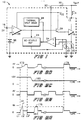
- Fig. 1 there is shown load driver circuit 10 in block diagram form for explaining the general operation of the preferred embodiment of the invention.
- driver circuit 10 which includes an internal power stage is fabricated in monolithic integrated circuit form.
- Output terminal 12 as shown may be coupled to one terminal of an external inductive coil 14, the other terminal of which is connected to a potential source VBAT. (It is understood that also a resistive load could be driven by driver circuit 10).
- inductive coil 14 is part of a fuel injection system, V BAT , would be the battery voltage and inductive coil 14 would be utilized to generate a magnetic field in response to a current conducted therethrough to operate the injector valves of the fuel injector system.
- an input signal generated in timed relationship to the operation of the automotive engine is applied to input terminal 16 to open and close the valves in response to the magnetic field produced by inductive coil 14.
- internal power stage 18 of the monolithic circuit is rendered full conductive so that maximum ramp current is generated through inductive coil 14.
- the current through sense resistor 20 which is coupled in series between power device 18 and ground reference is compared to the current through reference resistor 22 to limit the current through inductive coil 14 to a predetermined peak magnitude. Therefore, in response to an input signal applied to input terminal 16 (Fig.
- bistable reference circuit 24 is maintained at a first maximum level by comparator 34.
- comparator 34 When the current through inductive coil 14 reaches the peak magnitude, this condition is sensed across resistor 20 such that comparator 34 is caused to change states to source current away from transistor 28 and at the same time to cause bistable reference circuit 24 to switch states.
- This causes the current at the output of circuit 24 to be reduced to a lower or sustain level whereby the current conducted through conductive coil 14 is quickly reduced to this sustain level value as shown between time t2 and t3-t4.
- the input signal to circuit 10 goes to a low level state which turns off the driver circuit such that the current through inductive coil 14 is reduced to a zero level.
- the current produced through conductive coil 14 is referenced to an internal current provided in the driver circuit.
- Resistors 20 and 22 are shown within a dashed outline to indicate that these components are co-located within the monolithic circuit. Therefore, with these two components being fabricated of like material, for example, the same semiconductor material utilized in forming the emitter of transistor 28 these two resistors will have equal process variations and temperature characteristics. Hence, the switching characteristics of the system between the peak and sustaining current levels is not an absolute function of the voltages developed across these two resistors. Furthermore, by trimming resistor valves, process and temperature variations are eliminated between different integrated circuits. Typically, the ratio between the peak current level and the sustaining current level as shown in Fig. 2a is four to one.
- the input levels to circuit 10 are compatible with transistor-to-transistor logic (TTL) such that the circuit can be utilized with TTL logic circuitry.
- TTL transistor-to-transistor logic
- a thermal shutdown circuit 38 is shown for sensing the power dissipation in power device 18 to shut circuit 10 down if excessive power is dissipated in the power device. Thus damage to the integrated circuit is prevented.
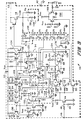
- FIG. 3 drive circuit 10 of the preferred embodiment is shown in complete detail. As shown, like components to components of Fig. 1 are referenced by the same numerals.
- Driver circuit 10 of Fig. 3 is shown included within a dashed outline form to indicate that all of the components therein are incorporated into a single monolithic integrated circuit chip.
- VCC terminal 32 is coupled to a source of operating potential such as a battery.
- Zener diode 40 is provided between terminal 32 and a ground reference terminal 42 which is adapted to be connected to ground reference potential. Zener diode 40 limits the operating potential for driver circuit 10 to a predetermined voltage level and protects the driver circuit from "load dump" transients which could otherwise occur if driver circuit 10 is utilized in the fuel injection system of an automobile, as is generally understood.
- driver circuit 10 is responsive to an input signal (Fig. 2b) supplied at input terminal 16 to drive conductive coil 14 at output terminal 12 as previously described.
- Fig. 2b an input signal supplied at input terminal 16 to drive conductive coil 14 at output terminal 12 as previously described.
- transistor 44 which has the base thereof coupled via resistor 46 to input terminal 16 is maintained in a non-conductive state.
- transistor 44 is biased via resistors 46 and 48 to a conducting level state.
- transistors 50, 52 and 54 each having their base electrodes coupled via resistors 56, 58 and 60 to the collector of transistor 44, are rendered conductive, being biased from power supply through resistor 62.
- the collectors of transistors 50, 52 and 54 will therefore be at near ground potential.
- the collector of transistor 50 acts to reset latch 64 comprising transistor 66 and 68 along with associated resistors.
- Transistor 66 will be maintained in a non-conductive state thereby supplying a "logic zero" at the output of the latch taken at node 70.
- the output of latch 64 which is coupled to bistable reference source 24, places the reference source in a first state to provide a first current level at the output thereof at node 72 to resistor 22 as will be described hereinafter.
- transistor 74 of bistable reference source 24 With latch 64 being in a reset state, transistor 74 of bistable reference source 24, which has its base coupled via resistor 76 to the output of the latch, is maintained in a non-conductive state which allows diode 78 to be forward biased.
- Transistors 80, 82, 84 and 86 which have their emitters respectively coupled to power supply terminal 32 through resistors 88-94, function as constant current sources to supply a current of the magnitude I at the respective collectors thereof.
- a current equal to a magnitude 41 is supplied at output node 72 to produce a reference current of 41 through resistor 22.
- This reference current through resistor 22 produces a reference voltage at the base of transistor 96, the non-inverting input of comparator 34.
- transistor 52 being in a conductive state, sinks the base current drive away from transistor 28 to maintain transistor 28 in a non-conductive state.
- transitor 44 is rendered conductive to turn off transistors 50, 52 and 54.
- transistor 28 With transistor 52 being in a non-conductive state transistor 28 is released and base current drive is provided thereto from transistors 102 and 104 which act as a base current source thereto.
- transistor 28 is rendered conductive and power stage 18 is driven into a saturated state to supply maximum output current at output terminal 12 as shown between time interval tl-t2 of Fig. 2a.
- power stage 18 is realized in integrated circuit form by a multi-emitter transistor having individual ballast resistors R b connected in series with each multi-emitter.
- power stage 18 may comprise a power device having 104 emitters with respective ballast resistors R b .
- 104 ballast resistors are utilized as indicated generally at 106, an equal percentage of total output current supplied at output terminal 12 will be conducted through each resistor.
- one of the ballast resistors, i.e., resistor 20 may be utilized to sense the current provided at output terminal 12 to compare this current with the reference current supplied through reference resistor 22 in order to determine when the current at output terminal 12 has reached a predetermined peak magnitude.
- bistable reference source 24 With bistable reference source 24 being in a state wherein a current of magnitude 41 is provided at output 72, a reference voltage is produced across reference resistor 22 and transistor 96 is rendered conductive as current is provided thereto from current source transistor 108.
- transistor 110 will be rendered conductive through current turnaround circuit 112 comprising diode 114 and transistor 116.
- Transistor 118 will be rendered non-conductive as are transistors 120 and 122.
- transistor 120 which is connected as a diode in series between transistor 118 and 122 and which has a collector output connected to the base of transistor 124 being non-conductive, transistor 124 is maintained in a non-conductive state wherein the collector thereof will be in a "logic one" state. Therefore, with transistor 120 being non-conductive, transistor 68 is maintained in a conductive state as previously described.
- Driver circuit 10 will remain in the aforedescribed state until such time that the current produced at output terminal 12 reaches a peak magnitude, at time t2, i.e., when the peak magnitude of current becomes substantially equal to the current provided at output 72 of reference source 24. At this time, if the output current at output terminal 12 tries to become greater than the value of the current supplied at the output of reference source 24 the gain of comparator amplifier 34 is great enough to rapidly cause transistor 110 as well as transistor 116 to be rendered non-conductive. As transistor 116 becomes non-conductive, transistor 118 is driven from transistor 108 rendering it conductive as well as transistors 120 and 122 connected in series therewith. As transistor 122 becomes conductive, base current drive is reduced to transistor 28 to reduce power drive to power device 18.
- the output current produced at output terminal 12 rapidly decreases to a second predetermined level between time interval t3-t4.
- the level to which the output current at output terminal 12 is reduced to is established by bistable reference source 24 in the following manner.
- transistor 120 becomes conductive current is supplied from the collector thereof through resistor 128. This causes transistor 124 to become conductive putting a "logic zero" at the set terminal of latch 64 to cause transistor 68 to become non-conductive.
- transistor 74 is rendered conductive to reverse bias diode 78. Therefore, with diode 74 reverse biased, transistor 86 provides the current output at output node 72 which now has a value of only I.
- the voltage across reference resistor 22 is reduced by a factor of four; this causes the current at output terminal 12 to be reduced until such time that the voltage produced across trim network 126 and sense resistor 20 (which is supplied to the base of transistor 110 of comparator 34) becomes equal to the new reference voltage produced across reference resistor 22 by the reduced current drive from the output of bistable reference source 24.
- the output from output terminal 12 will remain constant until time t4 when the input signal supplied to input terminal 16 of driver circuit 10 goes to a low level state which resets latch 64 to again forward bias diode 78 as previously discussed and to shunt base current drive away from transistor 28 through the collector emitter path of transistor 52.
- driver circuit 10 By co-locating reference resistor 22 with sense resistor 20 within the integrated circuit and by forming these two resistors of like semiconductor material, driver circuit 10 will function independently of temperature variations of the integrated circuit comprising the driver circuit. Also, by utilizing a resistive trim network between the inverting input of comparator 34 and the multiple emitters of the power transistor comprising power device 18, process variations can be eliminated by selective opening by laser or other means of links A. Therefore, the peak magnitude at which the driver circuit 10 is switched is set in production by monitoring the output current at output terminal 12 and trimming to the desired level by opening selective links A. Therefore, process variations between individual integrated circuit chips are eliminated by production trimming.
- a startup circuit comprising diode 130 connected in a current mirror configuration with transistor 132 is provided to ensure that driver circuit 10 becomes functional when the power supply potential is supplied thereto.
- diode 130 which is connected to the power supply rail via resistor 134 is instantly rendered conductive which turns transistor 132 on.
- the collector-to-emitter path provides a source for current for transistor 136 to render it conductive.
- the current source comprising transistors 138, 140 and 142 and associated resistors 144 and 146 are allowed to be biased up to set the current through current source transistors 80-86, 102, 104 and 108 as understood.
- the turn-on circuit comprising diode 130 and transistor 132 is rendered non-active by the feedback from transistor 108 via lead 148 to the emitter of transistor 132 which shuts this transistor off.
- the reference current source comprising transistors 138-142 is a well known ⁇ 0 current reference source wherein a A0 voltage (having a positive temperature coefficient) is established across resistor 146.
- Resistor 146 is fabricated of semiconductor material having a temperature coefficient which is substantially equal to the temperature coefficient of the voltage established thereacross such that the current produced through the collector-emitter of transistor 142 has a substantially zero temperature coefficient.
- the current produced at output node 72, from bistable reference current source 24 will also have a zero temperature coefficient. This is an important feature in that, although the resistor values of reference resistor 22 and sense resistor 20 may vary with temperature variations of driver circuit 10, the peak magnitude of output current at which the output current from driver circuit 10 is switched does not vary with temperature variations.
- thermal shutdown circuit 38 for preventing damage of the power stage 18.
- the novelty associated with thermal shutdown 38 relies in establishing a voltage at the base of transistor 150 which has a positive temperature coefficient that is a ratio of the positive temperature coefficient of the A0 voltage established across resistor 146.
- the current supplied through the collector of transistor 142 has a zero temperature coefficient and the output collector cuurent of transistor 108 via lead 148 also has a zero temperature coefficient, it is to be remembered that this current was generated from a voltage which had a positive temperature coefficient, i.e., the A0 voltage across resistor 146.
- the voltage developed across the resistor 152 also has a positive temperature coefficient, the mag - nitude thereof being a function of the ratio of the values of resistors 152 and 146.
- the voltage established at the base of transistor 150 will have the pre-determined positive temperature coefficient associated thereto.
- the integrated circuit in which driver circuit 10 is fabricated is caused to heat up by excessive power dissipation in power stage 18 a point will be reached that forward biases the base-to-emitter junction of transistor 150 to cause transistor 150 to become conductive.
- base current drive is shunted via resistor 154 from driver transistor 28 to reduce drive to the power stage which in turn then causes this stage to be turned off.
- Driver circuit 10 is therefore protected from becoming overheated by excessive power dissipation in power device 18.
- Circuit 156 which is controlled by an input signal supplied at control terminal 158 provides several unique functions as will be explained. If, for example, driver circuit 10 is to be utilized in fuel injection systems circuit 156 can be utilized to prevent damage to the injectors when the battery voltage of the automobile is sufficiently low. For instance, if the battery voltage is low (as shown by waveform portion 160 of Fig. 2c) there may not be enough voltage produced across inductive coil 14 to allow the current generated therethrough to ramp to the maximum peak magnitude as shown in Fig. 2a. For instance, if the peak magnitude is set at four amps, the low voltage across coil 14 may only allow the current supplied at output terminal 12 to ramp up to 3.99 amps.
- comparator 34 could not be activated to reduce the output current from driver circuit 10 to the low level as previously discussed.
- the current through coil 14 would remain at this high level and potentially damage the injectors.
- Circuit 156 is utilized in conjunction with a derived input signal at terminal 158 to cause the output of driver circuit 10 to be switched to the lower current level after a predetermined time if the peak magnitude of current therefrom has not been reached.
- Input terminal 158 may be coupled to an external RC network where the input signal produced thereat is the voltage developed across the capacitor.
- an external RC network By utilizing an external RC network the charging of the capacitor is independent of operation of driver circuit and is controlled by the RC time constant.
- transistor 54 With a zero level input signal at input terminal 16, transistor 54, as previously discussed, is rendered conductive which, via resistor 160, would cause discharge of the external capacitor to a zero voltage as shown at time t1 (Fig. 2d). With transistor 54 being conductive, transistor 168 is rendered conductive which causes the base of transistor 170 to be at low voltage level rendering this transistor non-conductive.
- transistor 54 is rendered non-conductive which allows the external capacitor to begin ramping upwards as shown by waveform portion 172 of Fig. 2d.
- the voltage level at terminal 158 will increase until such time that transistor 168 is rendered non-conductive which allows transistor 162 to become conductive.
- Transistor 162 is biased through resistors 164 and 166 to a voltage level compatible with TTL circuitry when V BAT is maximum. As transistor 162 becomes conductive, the current from the collector thereof renders transistor 170 conductive via resistor 174.
- Transistor 170 and transistor 124 are connected in an OR configuration such that with either one of these two transistors becoming conductive causes latch 64 to be set which as previously explained causes the output current at output terminal 12 of driver circuit 10 to be reduced to the lower level state.
- latch 64 the peak magnitude of current (time T2) has been reached previous to transistor 162 becoming conductive
- transistor 124 will have already set latch 64 and the output from driver circuit 10 is reduced at time t3 to its lower current level state.
- the battery voltage source is sufficiently low, as shown by waveform portion 160 of Fig. 2c, the output of driver circuit 10 will never reach the peak magnitude output. This is shown by waveform portion 176 of Fig. 2a.
- latch 64 cannot be set by transistor 124 whereby the output current level will remain at a constant level somewhere below the predetermined peak magnitude. Without circuit 156, the output current level of driver circuit 10 will remain constant. However, when the external capacitor is charged to the voltage level to render transistor 168 non-conductive, transistor 170 is rendered conductive to set the latch as shown at time t5 of Fig. 2a to reduce the output current level from driver circuit 10 to the lower current level.
- circuit 156 might be utilized in conjunction with a control voltage being supplied at input terminal 158 as shown by waveform portion 178. In this manner, the current level at output terminal 12 can be switched to its lower current level if the peak magnitude current level has not been reached by a predetermined time interval after the input signal at input terminal 16 has switched to its higher level state.
- circuit 10 By connecting input terminal 158 to input terminal 16, circuit 10 functions as a load protected integrated power switch.
- the output current provided at output 12 is fully conductive and constant, being set at any desired limit level within the dynamic range of trim network 126. If the load current exceeds the predetermined limit value the output (power stage 18) goes into an active state and thermal shutdown circuit 38 can protect the integrated circuit if excessive heating occurs as was previously described.
- the above described driver circuit for driving inductive or resistive loads is suitable to be fabricated entirely as an integrated circuit device including the power stage and functions by comparing a percentage of the load current to an internally generated reference current for switching the load current when a predetermined peak magnitude is reached to a constant, predetermined sustaining level.
Landscapes
- Engineering & Computer Science (AREA)
- Power Engineering (AREA)
- Electronic Switches (AREA)
- Relay Circuits (AREA)
Claims (2)
Applications Claiming Priority (2)
| Application Number | Priority Date | Filing Date | Title |
|---|---|---|---|
| US231550 | 1981-02-04 | ||
| US06/231,550 US4358812A (en) | 1981-02-04 | 1981-02-04 | Driver circuit for use with inductive loads or the like |
Publications (3)
| Publication Number | Publication Date |
|---|---|
| EP0070873A1 EP0070873A1 (de) | 1983-02-09 |
| EP0070873A4 EP0070873A4 (de) | 1985-07-30 |
| EP0070873B1 true EP0070873B1 (de) | 1990-11-28 |
Family
ID=22869701
Family Applications (1)
| Application Number | Title | Priority Date | Filing Date |
|---|---|---|---|
| EP82900602A Expired - Lifetime EP0070873B1 (de) | 1981-02-04 | 1982-01-04 | Mit induktiven lasten oder dergleichen verwendbarer steuerkreis |
Country Status (9)
| Country | Link |
|---|---|
| US (1) | US4358812A (de) |
| EP (1) | EP0070873B1 (de) |
| JP (1) | JPS58500046A (de) |
| BR (1) | BR8205839A (de) |
| CA (1) | CA1179732A (de) |
| DE (1) | DE3280269D1 (de) |
| IT (1) | IT1147581B (de) |
| MX (1) | MX150526A (de) |
| WO (1) | WO1982002794A1 (de) |
Families Citing this family (13)
| Publication number | Priority date | Publication date | Assignee | Title |
|---|---|---|---|---|
| DE3204234C2 (de) * | 1981-10-13 | 1985-08-29 | Erwin Sick Gmbh Optik-Elektronik, 7808 Waldkirch | Schaltungsanordnung zur Steuerung eines Relais |
| US4453194A (en) * | 1982-03-01 | 1984-06-05 | International Business Machines Corporation | Integrated power circuit with current sensing means |
| GB8406331D0 (en) * | 1984-03-10 | 1984-04-11 | Lucas Ind Plc | Control system |
| JPH0746651B2 (ja) * | 1984-12-18 | 1995-05-17 | 株式会社ゼクセル | ソレノイド駆動装置 |
| US4779062A (en) * | 1987-03-24 | 1988-10-18 | Cherry Semiconductor Corporation | Short circuit current limiter |
| US5045964A (en) * | 1990-04-30 | 1991-09-03 | Motorola, Inc. | Thermal clamp for an ignition coil driver |
| IT1241365B (it) * | 1990-12-21 | 1994-01-10 | Sgs Thomson Microelectronics | Circuito di pilotaggio di carichi induttivi, in particolare per iniettori di carburante |
| US5687050A (en) * | 1995-07-25 | 1997-11-11 | Ficht Gmbh | Electronic control circuit for an internal combustion engine |
| DE19920307A1 (de) * | 1999-05-03 | 2000-11-16 | St Microelectronics Gmbh | Elektrische Schaltung zum Steuern einer Last |
| EP1212771A1 (de) * | 1999-09-10 | 2002-06-12 | Intra International AB | Verfahren und vorrichtung zur steuerung der energieerzeugung und speicherung |
| US20040113494A1 (en) * | 2000-09-01 | 2004-06-17 | Karuppana Samy V. | Daytime running light control using an intelligent power management system |
| JP3587300B2 (ja) * | 2001-01-16 | 2004-11-10 | 株式会社デンソー | 集積回路装置 |
| JP6461427B2 (ja) * | 2016-03-30 | 2019-01-30 | アイシン・エィ・ダブリュ株式会社 | リニアソレノイド駆動装置 |
Citations (2)
| Publication number | Priority date | Publication date | Assignee | Title |
|---|---|---|---|---|
| US4180026A (en) * | 1976-03-26 | 1979-12-25 | Robert Bosch Gmbh | Apparatus for controlling the operating current of electromagnetic devices |
| DE2841781A1 (de) * | 1978-09-26 | 1980-04-10 | Bosch Gmbh Robert | Einrichtung zum betrieb von elektromagnetischen verbrauchern bei brennkraftmaschinen |
Family Cites Families (5)
| Publication number | Priority date | Publication date | Assignee | Title |
|---|---|---|---|---|
| JPS5413604A (en) * | 1977-07-01 | 1979-02-01 | Kajima Corp | Method of construction of closely building casing |
| US4234903A (en) * | 1978-02-27 | 1980-11-18 | The Bendix Corporation | Inductive load driver circuit effecting slow hold current delay and fast turn off current decay |
| DE2828678A1 (de) * | 1978-06-30 | 1980-04-17 | Bosch Gmbh Robert | Verfahren und einrichtung zum betrieb eines elektromagnetischen verbrauchers, insbesondere eines einspritzventils in brennkraftmaschinen |
| US4293888A (en) * | 1979-06-25 | 1981-10-06 | International Business Machines Corporation | Print hammer drive circuit with compensation for voltage variation |
| JPS5639368A (en) * | 1979-09-07 | 1981-04-15 | Hitachi Constr Mach Co Ltd | High speed driving circuit for solenoid valve |
-
1981
- 1981-02-04 US US06/231,550 patent/US4358812A/en not_active Expired - Lifetime
-
1982
- 1982-01-04 EP EP82900602A patent/EP0070873B1/de not_active Expired - Lifetime
- 1982-01-04 BR BR8205839A patent/BR8205839A/pt not_active IP Right Cessation
- 1982-01-04 WO PCT/US1982/000006 patent/WO1982002794A1/en not_active Ceased
- 1982-01-04 DE DE8282900602T patent/DE3280269D1/de not_active Expired - Lifetime
- 1982-01-04 JP JP57500603A patent/JPS58500046A/ja active Pending
- 1982-01-07 CA CA000393684A patent/CA1179732A/en not_active Expired
- 1982-02-02 IT IT47707/82A patent/IT1147581B/it active
- 1982-02-04 MX MX191276A patent/MX150526A/es unknown
Patent Citations (2)
| Publication number | Priority date | Publication date | Assignee | Title |
|---|---|---|---|---|
| US4180026A (en) * | 1976-03-26 | 1979-12-25 | Robert Bosch Gmbh | Apparatus for controlling the operating current of electromagnetic devices |
| DE2841781A1 (de) * | 1978-09-26 | 1980-04-10 | Bosch Gmbh Robert | Einrichtung zum betrieb von elektromagnetischen verbrauchern bei brennkraftmaschinen |
Also Published As
| Publication number | Publication date |
|---|---|
| WO1982002794A1 (en) | 1982-08-19 |
| MX150526A (es) | 1984-05-18 |
| CA1179732A (en) | 1984-12-18 |
| DE3280269D1 (de) | 1991-01-10 |
| US4358812A (en) | 1982-11-09 |
| EP0070873A1 (de) | 1983-02-09 |
| IT8247707A0 (it) | 1982-02-02 |
| JPS58500046A (ja) | 1983-01-06 |
| BR8205839A (pt) | 1983-01-11 |
| IT1147581B (it) | 1986-11-19 |
| EP0070873A4 (de) | 1985-07-30 |
Similar Documents
| Publication | Publication Date | Title |
|---|---|---|
| EP0008509B1 (de) | Steuerschaltungen für Elektromagnete | |
| EP0070873B1 (de) | Mit induktiven lasten oder dergleichen verwendbarer steuerkreis | |
| US5819713A (en) | Automotive ignition control system | |
| US6194884B1 (en) | Circuitry for maintaining a substantially constant sense current to load current ratio through an electrical load driving device | |
| US4319179A (en) | Voltage regulator circuitry having low quiescent current drain and high line voltage withstanding capability | |
| JPH02223672A (ja) | 半導体電力装置における過度の熱散逸に対して電流制御及び防護を与えるユニットのための診断回路 | |
| US5576648A (en) | Temperature stable circuit for controlled current discharge during the driving of an inductive load | |
| US4345296A (en) | Device for controlling the current through an inductive consumer, especially a magnetic valve in the fuel metering system of an internal combustion engine | |
| US20020109417A1 (en) | Driver circuit for soft turning on a power element connected to an inductive load | |
| US4359652A (en) | Over voltage detection circuit for use in electronic ignition systems | |
| US4723191A (en) | Electronic voltage regulator for use in vehicles with protection against transient overvoltages | |
| US6450157B1 (en) | Automotive ignition system with adaptable start-of-dwell ring damping | |
| US4555742A (en) | Short detection circuit and method for an electrical load | |
| USRE37778E1 (en) | Current limiting circuit | |
| EP0359851B1 (de) | Zündanlage für Innenverbrennungsmaschinen | |
| US4339781A (en) | Apparatus for controlling the electric current through an inductive consumer, in particular through a fuel metering valve in an internal combustion engine | |
| EP0773569A1 (de) | Treiberschaltung für eine Einspritzdüse | |
| US4574221A (en) | Ignition control integrated circuit having substrate injection preventing means | |
| US5105145A (en) | Voltage control circuit | |
| JP2568813Y2 (ja) | 内燃機関用点火装置 | |
| US4410808A (en) | Electrical circuit for driving a plurality of inductive loads | |
| US4381484A (en) | Transistor current source | |
| US7021299B2 (en) | Multichannel electronic ignition device with high-voltage controller | |
| US20010052775A1 (en) | Electronic ignition device | |
| JPH06501293A (ja) | 誘導負荷、例えば内燃機関の点火コイルを切り換えるためのダーリントン回路を備えた高出力段 |
Legal Events
| Date | Code | Title | Description |
|---|---|---|---|
| PUAI | Public reference made under article 153(3) epc to a published international application that has entered the european phase |
Free format text: ORIGINAL CODE: 0009012 |
|
| 17P | Request for examination filed |
Effective date: 19820925 |
|
| AK | Designated contracting states |
Designated state(s): DE FR GB SE |
|
| 17Q | First examination report despatched |
Effective date: 19860710 |
|
| GRAA | (expected) grant |
Free format text: ORIGINAL CODE: 0009210 |
|
| AK | Designated contracting states |
Kind code of ref document: B1 Designated state(s): DE FR GB SE |
|
| ET | Fr: translation filed | ||
| REF | Corresponds to: |
Ref document number: 3280269 Country of ref document: DE Date of ref document: 19910110 |
|
| PLBE | No opposition filed within time limit |
Free format text: ORIGINAL CODE: 0009261 |
|
| STAA | Information on the status of an ep patent application or granted ep patent |
Free format text: STATUS: NO OPPOSITION FILED WITHIN TIME LIMIT |
|
| 26N | No opposition filed | ||
| PGFP | Annual fee paid to national office [announced via postgrant information from national office to epo] |
Ref country code: FR Payment date: 19940126 Year of fee payment: 13 |
|
| PGFP | Annual fee paid to national office [announced via postgrant information from national office to epo] |
Ref country code: DE Payment date: 19940128 Year of fee payment: 13 |
|
| PGFP | Annual fee paid to national office [announced via postgrant information from national office to epo] |
Ref country code: SE Payment date: 19940131 Year of fee payment: 13 |
|
| PG25 | Lapsed in a contracting state [announced via postgrant information from national office to epo] |
Ref country code: SE Effective date: 19950105 |
|
| PGFP | Annual fee paid to national office [announced via postgrant information from national office to epo] |
Ref country code: GB Payment date: 19950126 Year of fee payment: 14 |
|
| EAL | Se: european patent in force in sweden |
Ref document number: 82900602.2 |
|
| PG25 | Lapsed in a contracting state [announced via postgrant information from national office to epo] |
Ref country code: FR Effective date: 19950929 |
|
| PG25 | Lapsed in a contracting state [announced via postgrant information from national office to epo] |
Ref country code: DE Effective date: 19951003 |
|
| EUG | Se: european patent has lapsed |
Ref document number: 82900602.2 |
|
| REG | Reference to a national code |
Ref country code: FR Ref legal event code: ST |
|
| PG25 | Lapsed in a contracting state [announced via postgrant information from national office to epo] |
Ref country code: GB Effective date: 19960104 |
|
| GBPC | Gb: european patent ceased through non-payment of renewal fee |
Effective date: 19960104 |