EP0071161A2 - Transistor mit kammförmiger Emitterstruktur - Google Patents
Transistor mit kammförmiger Emitterstruktur Download PDFInfo
- Publication number
- EP0071161A2 EP0071161A2 EP82106552A EP82106552A EP0071161A2 EP 0071161 A2 EP0071161 A2 EP 0071161A2 EP 82106552 A EP82106552 A EP 82106552A EP 82106552 A EP82106552 A EP 82106552A EP 0071161 A2 EP0071161 A2 EP 0071161A2
- Authority
- EP
- European Patent Office
- Prior art keywords
- region
- emitter
- mesh
- intersections
- emitter region
- Prior art date
- Legal status (The legal status is an assumption and is not a legal conclusion. Google has not performed a legal analysis and makes no representation as to the accuracy of the status listed.)
- Granted
Links
Images



Classifications
-
- H—ELECTRICITY
- H10—SEMICONDUCTOR DEVICES; ELECTRIC SOLID-STATE DEVICES NOT OTHERWISE PROVIDED FOR
- H10D—INORGANIC ELECTRIC SEMICONDUCTOR DEVICES
- H10D62/00—Semiconductor bodies, or regions thereof, of devices having potential barriers
- H10D62/10—Shapes, relative sizes or dispositions of the regions of the semiconductor bodies; Shapes of the semiconductor bodies
- H10D62/13—Semiconductor regions connected to electrodes carrying current to be rectified, amplified or switched, e.g. source or drain regions
- H10D62/133—Emitter regions of BJTs
-
- H—ELECTRICITY
- H10—SEMICONDUCTOR DEVICES; ELECTRIC SOLID-STATE DEVICES NOT OTHERWISE PROVIDED FOR
- H10D—INORGANIC ELECTRIC SEMICONDUCTOR DEVICES
- H10D84/00—Integrated devices formed in or on semiconductor substrates that comprise only semiconducting layers, e.g. on Si wafers or on GaAs-on-Si wafers
- H10D84/101—Integrated devices comprising main components and built-in components, e.g. IGBT having built-in freewheel diode
- H10D84/121—BJTs having built-in components
- H10D84/125—BJTs having built-in components the built-in components being resistive elements, e.g. BJT having a built-in ballasting resistor
Definitions
- This invention relates to a semiconductor device, particularly to a bipolar type transistor having the meshed plane pattern of emitter region.
- Overlay type transistors have a plurality of emitter regions formed in the form of lands in the vicinity of base region surface and said plurality of emitter regions are connected in parallel by the electrodes.
- Mesh emitter transistors have meshed emitter regions formed in the vicinity of base region surface and the electrodes are led from the intersections of said meshed portions.
- Ring emitter transistors have a plurality of ring-shaped emitters deposited in the form of lands in the vicinity of base region surface and said ring-shaped regions are connected in parallel by the electrodes.
- the periphery of the emitter region is made longer, as much as is possible, in the limitted base area in order to realize higher power and a higher frequency characteristic.
- This invention relates to an improvement in high power and high frequency transistors having said mesh emitter structure.
- Fig. l(b) is the sectional view along the line A-A' in Fig. l(a).
- n type emitter region 3 has the mesh type plane surface.
- 4 is the insulating film consisting of the silicon dioxide (SiO Z ) etc. covering the surface of silicon substrate; 5 is the base leadout electrode; 6 is the emitter leadout electrode; 7 is the collector electrode.
- 12a, 12b are base electrode windows provided on the insulating film 4 and 13a, 13b .... are emitter electrode windows provided on the insulating film 4.
- 14a, 14b, ... are P + type base contact region (base compensating diffused region).
- said mesh emitter transistor is requested to have a high breakdown voltage and a large safe operating area because it operates on a heavy current.
- the emitter strip of said mesh emitter transistor is widened in view of reducing a current density per unit area of the emitter region.
- the sectional area of base region is reduced due to enlargement of said emitter region and a resistance of base region under the emitter region 3, namely an internal base resistance rbb' in the direction from almost the center of the intersections of emitter strip to the base contact region 14, in other words, in the direction along the line A-A' of Fig.l(a), increases.
- Such increase of internal base resistance results in deterioration of switching speed of said mesh emitter transistor and moreover it causes a part of charges to remain just under the emitter strip on the occasion of the switching operation, particularly of the turn-off, thereby allowing concentration of a current and resultant breakdown of said mesh emitter transistor.
- the present invention provides a semiconductor device characterized in that the collector region has a first coductivity type, the base region has a second conductivity type formed in said collector region and the mesh emitter region of the first conductivity type formed in said base region and making inactive electrically the center area of the intersections in said mesh emitter region.
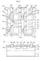
- 101 is the n type silicon (Si) substrate forming the collector region;
- 102 is the P type base region formed by diffusing selectively or entirely the acceptor impurity, for example, the boron (B) into the one main surface of said silicon substrate 101;
- 103 is the n + type emitter region formed by selectively diffusing the donor impurity, for example, the phosphorus (P) into said P type base region 102.
- such n + type emitter region 103 has the mesh plane surface and said emitter region is not formed in almost the center of the intersections of mesh structure and a part 102' of the base region 102 is exposed. Namely, the intersecting areas of the emitter region 103 are hollowed.
- 104 is the insulating film consisting of the silicon dioxide (Si0 2 ) which covers the surface of silicon substrate, 105 is the base leadout electrode consisting of the aluminium (Al), 106 is the emitter leadout electrode also consisting of the aluminium and 107 is the collector electrode.
- a plurality of base leadout electrodes 105 are connected in common to the base electrode pad 108, and a plurality of emitter leadout electrodes 106 are also connected in common to the emitter electrode pad 109.
- 112a, 112b, ... are base electrode windows provided in the insulating film 104; 113a, 113b ... are emitter electrode windows provided also in the insulating film 104.
- 114a, 114b, ... are p + type base contact region (base compensating diffused region).
- the emitter region is hollowed at the center of intersections in the mesh emitter region 103 as explained previously and there by a part 102' of the base region is exposed.
- a base resistance in said base region 102' is sufficiently low because said base region 102' is thick and therefore a base resistance just under the emitter region 103 along the line B-B' is substantially equal to a resistance of base region 102 just under said emitter region 103.
- an internal base resistance rbb' can drastically be reduced as compared with that of said conventional structure.
- a semiconductor device having such mesh emitter structure is capable of realizing improvement in the switching speed. Further, when said internal base resistance rbb' is reduced, the amount of charges which remain in the area just under the emitter region 103 at the time of turn-off and also are accumulated therein can also be reduced, making less the current concentration to the intersections of said emitter region 103.
- a current to be concentrated to the intersections in the emitter region at the time of turn-off is diverged to the circumference of the emitter region 103 which is in contact with the base region 102'.
- a mesh emitter transistor having the structure shown in Fig. 2 is formed, wherein
- the safe operating area in the reverse bias has been measured under the load of inductance (L) for the mesh emitter transistor of conventional structure and that of the present invention.
- the safe operation current of both transistors has been obtained under the condition that the load inductance is 1 mH and collector-emitter voltage is 900V.
- the safe operation current of the conventional mesh emitter transistor was 3 ampere, while that of the mesh emitter transistor of the present invention was 6 ampere. Namely, the safe operating area can be increased outstandingly by the present invention.
- Fig. 8 shows the reverse bias safe operating areas of such conventional mesh emitter transistor and the mesh emitter transistor of the present invention.
- a collector current (Ic) is plotted on the vertical axis, while the collector-emitter voltage (V CE ) is platted on the horizontal axis.
- the measuring conditions are as follows; a load inductance value is 1 mH, a collector voltage is 60 V, a base current (IB 2 ) for pulling to OFF from ON is -1 ampere, a base current for pulling to OFF from ON is about 5 V.
- the area enclosed by the X axis, the Y axis, the points F 1 , p 2 , P 3 and P 4 is the reverse bias safe operating area of the conventional mesh emitter transistor
- the area enclosed by the X axis, the Y axis, the points P l1 P 111 p 12' p 4 is the reverse bias safe operating area of the mesh emitter transistor of the present invention.
- the fall time of said conventional mesh emitter transistor was 120 ns, while the fall time of the mesh emitter transistor of the present invention was 70 ns. Namely, the present invention has realized a drastic improvement in the switching characteristic.
- the present invention is capable of providing a semiconductor device ensuring excellent high speed switching characteristic and a large safe operating area which could not be obtained in said conventional mesh emitter transistor.
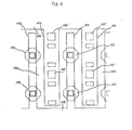
- Fig. 3 is the second embodiment of the semiconductor device of the present invention.
- the portions corresponding to those in the embodiment of Fig. 2 are given the same numbering or symbols.
- intersections of mesh emitter region are widely located in the direction to base electrode window 105.
- the emitter region increases its area because it is widely arranged in the direction to the base electrode window, allowing an emitter current to increase. Thereby a semiconductor device for a higher power can be formed.
- Fig. 4 is the third embodiment of the semiconductor device of the present invention.
- the portions corresponding to those in Fig. 2 are given the same numbering or symbols.
- the emitter electrode window 113 is formed on the insulating film 104 in such a manner as to surround the base region 102'.
- the electrode can be made with a lower resistance.
- Fig. 5 is the fourth embodiment of the semiconductor device of the present invention.
- the portions corresponding to those in Fig. 2 are given the same numbering or symbols.
- the emitter ballast resistors are respectively deposited at the intersections of mesh emitter region 103 and the emitter leadout electrode 106 is connected to the emitter region 103 via said emitter ballast resistors.
- the base region 102' exposed at the center of intersections in the mesh emitter region 103 has the octagonal plane surface and the exposed area of the base region 102 also has the octagonal shape.
- 151 is the emitter ballast resistor, consisting, for example, of the polycrystalline silicon containing impurity such as phosphorus or nichrome (Ni-Cr) etc.; 152 is the connecting conductor consisting of aluminium, for example, connecting between said emitter ballast resistor 151 and the emitter region 102 via the emitter electrode window 113.
- the ballast resistor 151 is provided and connected with the emitter electrodes (for example 106a und 106b) at both ends and also provided and connected with the connecting conductor 152 at its center area.
- a resistance value of the ballast resistor 151 is determined by selecting the thickness, width or impurity concentration.
- said ballast resistor 151 is formed by deposition of the polycrystalline silicon including the phosphorus(P), for example, and succeeding patterning process utilizing the photolithography technique.
- the base leadout electrode, emitter leadout electrode and connecting conductor are formed by deposition of aluminium and successive patterning process in accordance with the ordinary planar bipolar transistor producing processes.
- ballast resistors 151 are arranged in the intersections of the mesh emitter region 103, in order to give a connection by said ballast resistor between the emitter leadout electrode and the emitter region, the emitter region operates uniformly in any portion even when it operates on any heavy current, not allowing concentration of a current to a particular portion.
- said semiconductor device does not result in breakdown due to the secondary breakdown phenomenon, assuring an excellent high frequency characteristic, a high speed switching characteristic and a large safe operating area.
- the polycrystalline silicon layer, for example, forming the ballast resistor 151 is partly placed in contact with the emitter region 106.
- the present invention is not limited thereto. It is also possible to allow the resistance material forming such ballast resistor to be extended under the emitter electrode 106 and the emitter electrode pad 109. Such resistance meterial extending thereunder improves flatness in the semiconductor substrate surface and raises accuracy of photo-etching and production yield on the occasion of forming the emitter electrode 106 and emitter electrode pad 109.
- Fig. 6 shows the fifth embodiment of the semiconductor device of the present invention. It indicates the same sectional view as Fig. 2(b). The portions corresponding to those in the embodiment of Fig. 2 are given the same numbering or symbols.
- the center is selectively shallowed at the intersections of mesh emitter region.
- the shallowed emitter region 103a becomes inactive electrically as compared with the surrounding emitter region 103.
- the base region 102 under said emitter region 103a is wide (or deeper), and therefore, a base resistance in such area is small. Therefore, on the occasion of the switching operation of said semiconductor device, the amount of charges remaining under the emitter region 103a is reduced and current concentration in the intersections in the emitter region 103 is restricted.
- Fig. 7 shows the sixth embodiment of the semiconductor device of the present invention.
- Fig. 7 indicates the sectional view similar to said Fig. 2(b).
- the portions corresponding to those in Fig. 2 are given the same numbering or symbol.
- the opposite conductivity type regions (P type region) 171 are deposited selectively almost at the center of said emitter region in the intersections of mesh emitter region.
- the emitter region 103b under such opposite conductivity type region 171 becomes substantially inactive.
- a semiconductor device of the present invention indicated in Fig. 2 to Fig. 7 can be formed with ordinary planar type bipolar transistor production method.
- impurity concentration and depth of the base region, emitter region and collector region, moreover thickness of surface insulating film and thickness of electrode material are selected by the power and frequency of the pertinent semiconductor device.
- a semiconductor device having the high speed switching characteristic and a large safe operating area can be realized by exposing the base regin without forming the emitter region at the center of intersections in the mesh emitter region. Therefore, reduction in size and weight of switching power supply can be realized by introducing such semiconductor device into the switching power supply.
Landscapes
- Bipolar Transistors (AREA)
Applications Claiming Priority (2)
| Application Number | Priority Date | Filing Date | Title |
|---|---|---|---|
| JP56118154A JPS5818964A (ja) | 1981-07-28 | 1981-07-28 | 半導体装置 |
| JP118154/81 | 1981-07-28 |
Publications (3)
| Publication Number | Publication Date |
|---|---|
| EP0071161A2 true EP0071161A2 (de) | 1983-02-09 |
| EP0071161A3 EP0071161A3 (en) | 1983-11-16 |
| EP0071161B1 EP0071161B1 (de) | 1987-10-14 |
Family
ID=14729426
Family Applications (1)
| Application Number | Title | Priority Date | Filing Date |
|---|---|---|---|
| EP82106552A Expired EP0071161B1 (de) | 1981-07-28 | 1982-07-21 | Transistor mit kammförmiger Emitterstruktur |
Country Status (4)
| Country | Link |
|---|---|
| US (1) | US4586072A (de) |
| EP (1) | EP0071161B1 (de) |
| JP (1) | JPS5818964A (de) |
| DE (1) | DE3277484D1 (de) |
Cited By (3)
| Publication number | Priority date | Publication date | Assignee | Title |
|---|---|---|---|---|
| EP0343879A3 (en) * | 1988-05-20 | 1990-08-16 | General Electric Company | Bipolar transistor |
| EP0691034A4 (de) * | 1993-03-25 | 1996-03-13 | Micrel Inc | Bipolartransistorstruktur mit ballastwiderstand |
| WO2000028599A1 (en) * | 1998-11-06 | 2000-05-18 | International Business Machines Corporation | Transistor array |
Families Citing this family (12)
| Publication number | Priority date | Publication date | Assignee | Title |
|---|---|---|---|---|
| JPS60165759A (ja) * | 1984-02-07 | 1985-08-28 | Nippon Denso Co Ltd | 集積回路素子 |
| JPH0442918Y2 (de) * | 1986-04-17 | 1992-10-12 | ||
| US4775879A (en) * | 1987-03-18 | 1988-10-04 | Motorola Inc. | FET structure arrangement having low on resistance |
| US5298785A (en) * | 1987-05-15 | 1994-03-29 | Fuji Electric Co., Ltd. | Semiconductor device |
| FR2615326B1 (fr) * | 1987-05-15 | 1990-08-31 | Fuji Electric Co Ltd | Dispositif a semi-conducteurs du type multi-emetteur |
| JPH0712045B2 (ja) * | 1988-03-02 | 1995-02-08 | 株式会社東海理化電機製作所 | 電流検出素子 |
| US5341020A (en) * | 1991-04-12 | 1994-08-23 | Sanken Electric Co., Ltd. | Integrated multicellular transistor chip for power switching applications |
| JP2974452B2 (ja) * | 1991-06-19 | 1999-11-10 | キヤノン株式会社 | 磁性トナー |
| JP2006049693A (ja) * | 2004-08-06 | 2006-02-16 | Matsushita Electric Ind Co Ltd | 半導体装置 |
| KR101159997B1 (ko) | 2010-09-29 | 2012-06-25 | 현대제철 주식회사 | 홀확장성이 우수한 저탄소 고강도 열연강판 및 그 제조 방법 |
| US20190181251A1 (en) * | 2017-12-07 | 2019-06-13 | Qualcomm Incorporated | Mesh structure for heterojunction bipolar transistors for rf applications |
| CN113594239B (zh) * | 2021-07-20 | 2022-09-27 | 弘大芯源(深圳)半导体有限公司 | 一种具有网格结构的双极功率晶体管 |
Family Cites Families (16)
| Publication number | Priority date | Publication date | Assignee | Title |
|---|---|---|---|---|
| DE1297239C2 (de) * | 1964-11-11 | 1975-07-17 | Deutsche Itt Industries Gmbh, 7800 Freiburg | Leistungstransistor |
| GB1153497A (en) * | 1966-07-25 | 1969-05-29 | Associated Semiconductor Mft | Improvements in and relating to Semiconductor Devices |
| DE1614800C3 (de) * | 1967-04-08 | 1978-06-08 | Telefunken Patentverwertungsgesellschaft Mbh, 7900 Ulm | Verfahren zum Herstellen eines Planartransistors mit Tetrodeneigenschaften |
| NL6712617A (de) * | 1967-09-15 | 1969-03-18 | ||
| NL164703C (nl) * | 1968-06-21 | 1981-01-15 | Philips Nv | Halfgeleiderinrichting, voorzien van een contact met ten minste twee gedeelten en een voor deze gedeelten gemeenschappelijk gedeelte, waarbij in elk der ver- bindingswegen tussen de gedeelten en het gemeenschappe- lijke gedeelte een serieweerstand is opgenomen. |
| US3609460A (en) * | 1968-06-28 | 1971-09-28 | Rca Corp | Power transistor having ballasted emitter fingers interdigitated with base fingers |
| US3600646A (en) * | 1969-12-18 | 1971-08-17 | Rca Corp | Power transistor |
| JPS586307B2 (ja) * | 1976-12-16 | 1983-02-03 | 富士電機株式会社 | 半導体装置 |
| FR2374742A1 (fr) * | 1976-12-20 | 1978-07-13 | Radiotechnique Compelec | Transistor multicouche pour tensions elevees et son procede de fabrication |
| JPS5477586A (en) * | 1977-10-25 | 1979-06-21 | Gen Electric | Semiconductor |
| JPS54117689A (en) * | 1978-03-03 | 1979-09-12 | Mitsubishi Electric Corp | Semiconductor device |
| JPS54120587A (en) * | 1978-03-10 | 1979-09-19 | Fujitsu Ltd | Transistor |
| GB2026236B (en) * | 1978-07-20 | 1983-02-02 | Gen Electric | Power transistor |
| JPS55150271A (en) * | 1979-05-11 | 1980-11-22 | Hitachi Ltd | Semiconductor device |
| EP0059720A1 (de) * | 1980-09-12 | 1982-09-15 | Motorola, Inc. | Emitterstruktur für leistungstransistoren mit verbessertem funktionsbereich bei inverser polung und mit verbessertem schaltverhalten |
| DE3035462A1 (de) * | 1980-09-19 | 1982-05-13 | Siemens AG, 1000 Berlin und 8000 München | Halbleiterelement |
-
1981
- 1981-07-28 JP JP56118154A patent/JPS5818964A/ja active Granted
-
1982
- 1982-07-21 EP EP82106552A patent/EP0071161B1/de not_active Expired
- 1982-07-21 DE DE8282106552T patent/DE3277484D1/de not_active Expired
- 1982-07-28 US US06/402,425 patent/US4586072A/en not_active Expired - Fee Related
Cited By (5)
| Publication number | Priority date | Publication date | Assignee | Title |
|---|---|---|---|---|
| EP0343879A3 (en) * | 1988-05-20 | 1990-08-16 | General Electric Company | Bipolar transistor |
| EP0691034A4 (de) * | 1993-03-25 | 1996-03-13 | Micrel Inc | Bipolartransistorstruktur mit ballastwiderstand |
| WO2000028599A1 (en) * | 1998-11-06 | 2000-05-18 | International Business Machines Corporation | Transistor array |
| US6423603B2 (en) | 1998-11-06 | 2002-07-23 | International Business Machines Corporation | Method of forming a microwave array transistor for low-noise and high-power applications |
| US6762479B2 (en) | 1998-11-06 | 2004-07-13 | International Business Machines Corporation | Microwave array transistor for low-noise and high-power applications |
Also Published As
| Publication number | Publication date |
|---|---|
| DE3277484D1 (en) | 1987-11-19 |
| EP0071161A3 (en) | 1983-11-16 |
| US4586072A (en) | 1986-04-29 |
| JPH0156531B2 (de) | 1989-11-30 |
| EP0071161B1 (de) | 1987-10-14 |
| JPS5818964A (ja) | 1983-02-03 |
Similar Documents
| Publication | Publication Date | Title |
|---|---|---|
| EP0071161A2 (de) | Transistor mit kammförmiger Emitterstruktur | |
| US4642674A (en) | Field effect semiconductor device having improved voltage breakdown characteristics | |
| US4188707A (en) | Semiconductor devices and method of manufacturing the same | |
| US3944447A (en) | Method for fabrication of integrated circuit structure with full dielectric isolation utilizing selective oxidation | |
| EP0016577B1 (de) | Integrierte Halbleiter-Schaltungsvorrichtung mit doppelter Verbindungsschicht | |
| SE457035B (sv) | Mosfet-anordning foer hoegspaenningsbruk. | |
| EP0623951B1 (de) | Halbleiteranordnung in einer dünnen aktiven Schicht mit hoher Durchbruchspannung | |
| KR900004728B1 (ko) | 고 내압 반도체 장치 및 그의 제조방법 | |
| US4536784A (en) | Semiconductor device having a junction capacitance, an integrated injection logic circuit and a transistor in a semiconductor body | |
| EP0020929A1 (de) | Feldeffekttransistoren | |
| US4399451A (en) | Semiconductor device and method for production thereof | |
| US4179793A (en) | Method of making a charge transfer device | |
| US4742021A (en) | Subsurface zener diode and method of making | |
| JPH01123476A (ja) | 半導体装置およびその製法 | |
| US4835588A (en) | Transistor | |
| US4766469A (en) | Integrated buried zener diode and temperature compensation transistor | |
| US4261003A (en) | Integrated circuit structures with full dielectric isolation and a novel method for fabrication thereof | |
| HK1008116B (en) | Zener diode | |
| JPH02208952A (ja) | 半導体装置及びその製造方法 | |
| US5314836A (en) | Method of making a single electrode level CCD | |
| US3617826A (en) | An integrated transistor with a polycrystalline contact to a buried collector region | |
| EP0064614A2 (de) | Emitterstruktur für Halbleiteranordnungen | |
| EP0024923B1 (de) | Transistor Struktur | |
| US4328611A (en) | Method for manufacture of an interdigitated collector structure utilizing etch and refill techniques | |
| JPS6048111B2 (ja) | 不揮発性半導体記憶装置 |
Legal Events
| Date | Code | Title | Description |
|---|---|---|---|
| PUAI | Public reference made under article 153(3) epc to a published international application that has entered the european phase |
Free format text: ORIGINAL CODE: 0009012 |
|
| AK | Designated contracting states |
Designated state(s): DE FR GB |
|
| PUAL | Search report despatched |
Free format text: ORIGINAL CODE: 0009013 |
|
| AK | Designated contracting states |
Designated state(s): DE FR GB |
|
| 17P | Request for examination filed |
Effective date: 19831129 |
|
| GRAA | (expected) grant |
Free format text: ORIGINAL CODE: 0009210 |
|
| AK | Designated contracting states |
Kind code of ref document: B1 Designated state(s): DE FR GB |
|
| REF | Corresponds to: |
Ref document number: 3277484 Country of ref document: DE Date of ref document: 19871119 |
|
| ET | Fr: translation filed | ||
| PLBE | No opposition filed within time limit |
Free format text: ORIGINAL CODE: 0009261 |
|
| STAA | Information on the status of an ep patent application or granted ep patent |
Free format text: STATUS: NO OPPOSITION FILED WITHIN TIME LIMIT |
|
| 26N | No opposition filed | ||
| PGFP | Annual fee paid to national office [announced via postgrant information from national office to epo] |
Ref country code: FR Payment date: 19960709 Year of fee payment: 15 |
|
| PGFP | Annual fee paid to national office [announced via postgrant information from national office to epo] |
Ref country code: GB Payment date: 19960712 Year of fee payment: 15 |
|
| PGFP | Annual fee paid to national office [announced via postgrant information from national office to epo] |
Ref country code: DE Payment date: 19960726 Year of fee payment: 15 |
|
| PG25 | Lapsed in a contracting state [announced via postgrant information from national office to epo] |
Ref country code: GB Free format text: LAPSE BECAUSE OF NON-PAYMENT OF DUE FEES Effective date: 19970721 |
|
| GBPC | Gb: european patent ceased through non-payment of renewal fee |
Effective date: 19970721 |
|
| PG25 | Lapsed in a contracting state [announced via postgrant information from national office to epo] |
Ref country code: FR Free format text: LAPSE BECAUSE OF NON-PAYMENT OF DUE FEES Effective date: 19980331 |
|
| PG25 | Lapsed in a contracting state [announced via postgrant information from national office to epo] |
Ref country code: DE Free format text: LAPSE BECAUSE OF NON-PAYMENT OF DUE FEES Effective date: 19980401 |
|
| REG | Reference to a national code |
Ref country code: FR Ref legal event code: ST |