EP0072622A2 - Système économiseur d'énergie fournissant une commande de courant - Google Patents
Système économiseur d'énergie fournissant une commande de courant Download PDFInfo
- Publication number
- EP0072622A2 EP0072622A2 EP82303651A EP82303651A EP0072622A2 EP 0072622 A2 EP0072622 A2 EP 0072622A2 EP 82303651 A EP82303651 A EP 82303651A EP 82303651 A EP82303651 A EP 82303651A EP 0072622 A2 EP0072622 A2 EP 0072622A2
- Authority
- EP
- European Patent Office
- Prior art keywords
- voltage
- transistor
- control system
- electrical control
- current
- Prior art date
- Legal status (The legal status is an assumption and is not a legal conclusion. Google has not performed a legal analysis and makes no representation as to the accuracy of the status listed.)
- Withdrawn
Links
Images


Classifications
-
- H—ELECTRICITY
- H05—ELECTRIC TECHNIQUES NOT OTHERWISE PROVIDED FOR
- H05B—ELECTRIC HEATING; ELECTRIC LIGHT SOURCES NOT OTHERWISE PROVIDED FOR; CIRCUIT ARRANGEMENTS FOR ELECTRIC LIGHT SOURCES, IN GENERAL
- H05B39/00—Circuit arrangements or apparatus for operating incandescent light sources
- H05B39/04—Controlling
- H05B39/041—Controlling the light-intensity of the source
- H05B39/044—Controlling the light-intensity of the source continuously
- H05B39/048—Controlling the light-intensity of the source continuously with reverse phase control
-
- H—ELECTRICITY
- H05—ELECTRIC TECHNIQUES NOT OTHERWISE PROVIDED FOR
- H05B—ELECTRIC HEATING; ELECTRIC LIGHT SOURCES NOT OTHERWISE PROVIDED FOR; CIRCUIT ARRANGEMENTS FOR ELECTRIC LIGHT SOURCES, IN GENERAL
- H05B41/00—Circuit arrangements or apparatus for igniting or operating discharge lamps
- H05B41/14—Circuit arrangements
- H05B41/36—Controlling
- H05B41/38—Controlling the intensity of light
- H05B41/39—Controlling the intensity of light continuously
- H05B41/392—Controlling the intensity of light continuously using semiconductor devices, e.g. thyristor
- H05B41/3921—Controlling the intensity of light continuously using semiconductor devices, e.g. thyristor with possibility of light intensity variations
- H05B41/3924—Controlling the intensity of light continuously using semiconductor devices, e.g. thyristor with possibility of light intensity variations by phase control, e.g. using a triac
-
- Y—GENERAL TAGGING OF NEW TECHNOLOGICAL DEVELOPMENTS; GENERAL TAGGING OF CROSS-SECTIONAL TECHNOLOGIES SPANNING OVER SEVERAL SECTIONS OF THE IPC; TECHNICAL SUBJECTS COVERED BY FORMER USPC CROSS-REFERENCE ART COLLECTIONS [XRACs] AND DIGESTS
- Y10—TECHNICAL SUBJECTS COVERED BY FORMER USPC
- Y10S—TECHNICAL SUBJECTS COVERED BY FORMER USPC CROSS-REFERENCE ART COLLECTIONS [XRACs] AND DIGESTS
- Y10S315/00—Electric lamp and discharge devices: systems
- Y10S315/04—Dimming circuit for fluorescent lamps
Definitions
- the present invention relates to an electrical control system for controlling the current flow from an AC voltage supply to an electrical load, said control system comprising electronic switching means connected to said load so as to provide a controlled current path to the load, for providing for the application of substantially the entire available AC input voltage to the load during an initial portion of the AC supply voltage half wave.
- the invention is particularly, but not exclusively, applicable to fluoroescent and incandescent lamps.
- a gas discharge lamp and its associated ballast form one of the most recalcitrant systems to control and the present invention provides specific advantages in this regard. Accordingly, the present invention will basically be described in connection with its use in such a system to illustrate the control capabilities of the invention. However, it will be understood that the invention is applicable to other lamp systems, e.g. incandescent lamps, and to other electrical load devices.
- a gas discharge lamp and the light output therefrom are difficult to control due to the phenomena associated with the conduction of electricity through gas.
- a lamp requires at least an electron emitter and an electron collector, i.e. a cathode and an anode (the lamp electrodes), and a suitable gas ion population contained within the lamp envelope.
- the electrodes When a sufficiently high instantaneous voltage differential exists between the electrodes, electrons will flow from the cathode to the anode through the gas ion column. In so doing, the electrons collide with the gas ions, ultimately causing photons to be emitted.
- the wavelengths of these photons depend on the molecular structure of the gas. In some gas discharge lamps these arc generated photons are used directly for illumination.
- the arc generated photons are primarily used to strike and, in turn, excite the phosphor molecules coated on the inside of the glass envelope of the lamp.
- the excited phosphors in turn emit longer wavelength photons in the visual spectrum band. This process is sometimes called fluorescence.
- the second major problem concerns the fact that the gas conducts only after arc ignition, and this only occurs during the higher amplitude portion of the voltage sine wave. This factor rules out voltage control except for a relatively narrow range because the arc drops out of conduction at around 75% of the r.m.s. line voltage.
- the third major problem is that the lamp cathodes must be properly heated.
- the cathodes must be heated so that electrons are readily available as current carriers for the arc to conduct. Normally, this heating is accomplished by the arc itself and/or by transformer heater windings. It is important to note that if the cathodes are not kept at the required thermionic emission temperature, the useful lamp life can be substantially shortened.
- the American National Standards Institute ANSI
- the cathode heating voltage of rapid start lamps is provided by voltage taps on the secondary winding of the rapid start ballast.
- the ballast also provides the voltage transformation and inductance necessary to strike and limit the arc current, respectively.
- thyristors i.e. SCRs and TRIACs
- control techniques were developed that could limit the on-time of the arc current within each half wave of the AC voltage sine wave. This techniques provides an apparent dimming effect.
- the cathode heating time is also limited and as a consequence the cathodes are not properly heated.
- thyristor dimming ballasts were developed which include independent cathode heating windings. With a dimming ballast, the thyristor only controls the ballast winding associated with the lamp arc.
- This type of control can be characterised as being off at the beginning of each voltage half wave and being turned on at some point in time during the voltage half wave. The thyristor then remains on until near the end of the voltage half wave (zero crossover) when there is insufficient holding current to keep the thyristor turned on.
- the transistor when the current reaches the preset value, the transistor is switched from the saturated full-on state to the active or limiting region of transistor operation for part of the remaining time period of the voltage half wave. If the minimum current is all that is required, then the transistor remains in the active region until the excess voltage declines to that required by the arc. At this time the transistor again is saturated full-on until the voltage declines to zero. The process is repeated in the next half cycle. If more average current is required, and this is preferably related to the level of light output, the transistor is ther switched full-on before the end of the period of active current limiting transistor operation. Hence, the time of active transistor operation can be varied within each voltage half wave and thus the light output can be varied from a minimum to maximum level.
- the transistor must absorb some of the instantaneous ballast voltage.
- the product of the voltage appearing across the collector and emitter of the transistor and the minimum or preset current flowing in the transistor emitter is energy which must be dissipated by this transistor.
- the exact amount of dissipated energy will, of course, vary, depending on the time period within each half wave that the transistor is operating in the active region.
- the control provided by the ECALO system can therefore be described as a dissipative system which utilizes at least a minimum-on current in the earlier part of the time period of each voltage half wave which may be followed with a time controlled, full-on load compliance current during the latter portion of the voltage half wave.
- the present control system is characterised in that said switching means provides for switching off this input voltage at a variable point in time during said AC supply voltage half wave; and in that the control system further comprises capacitor means, comprising a capacitor connected so as to provide an alternate current path to the load when said input voltage is switched off by said electronic switching means,for sustaining the current flow to the load when said input voltage is switched off by said electronic switching means.
- control system eliminates the need for active region transistor operation and may improve the power factor of the electrical load device.
- the control provided by the invention differs from either the thyristor or ECALO-type control systems discussed above by producing a full-on load compliance current beginning in the early part of the time period of each voltage half wave.
- the electronic switching means preferably comprises a transistor, and control means for turning said transistor full-on during said initial portion of the AC supply voltage half wave and for turning said transistor off at a said variable point in time.
- the full-on current flowing through the control transistor can then be terminated at any point in time within the voltage half wave without interrupting the current flowing in the ballast primary, or other load device, because an alternate reactive current path is provided through the capacitor means. Therefore, the current continues flowing, through this alternative path, even though the transistor is turned off.
- the load current continues to flow but begins to limit as the capacitor charges during the latter portions of the time frame for each AC half wave, and the r.m.s. current level during each half wave is controlled by the time period of the full-on transistor during the leading portion of the voltage half wave.
- ballast voltage across the ballast corresponds to only that portion of the source voltage present after the switch is turned on (S on ) ' Because the ballast voltage of a thyristor controlled system may be substantially reduced, a special dimming ballast is required to insure that there is heater winding voltage during the full range of control.
- the ECALO control system provides for a minimum-on current followed by a time varying full-on load compliance current and the full-on portion of the ECALO current flows towards the end of each voltage half wave.
- T A the portion of time that the control transistor of the ECALO system is operating in the active region
- the system is dissipating a relatively substantial amount of energy (the product of the T A voltage and the T A current over the time period during which the two contemporaneously exist).
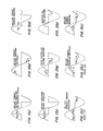
- the R.M.S. voltage reaching the ballast is much greater than that of a thyristor control system, as can be seen by comparing Figure 2(a) and Figure l(a).
- the ballast voltage of an ECALO equipped system is always of sufficient value to provide the heater windings of a standard vallast with sufficient source voltage to provide the lamp cathodes with the necessary lamp firing voltage followed by the relatively small (2.5V) sustaining voltage required to keep the cathodes at a minimum thermionic emission temperature.
- the cathode temperatures are sufficient to emit electrons without shortening lamp life.
- the arc current flows over the entire time frame that current can be conducted within the AC half wave, the current is less lagging than in a thyristor control system and, therefore, an ECALO system may require less power factor correction than a thyristor control system.
- the present system is non-dissipative, except for the switching tansition time and passive circuit element losses but unlike a thyristor control system, the full-on load compliance current tends to flow more toward the beginning of the AC voltage sine wave (see Figure 3(c)).
- the control transistor employed in this system when used to conduct current, is always saturated full-on starting at the beginning of the AC voltage sine wave. Therefore, a full-on load compliance current is provided earlier in the half wave time frame than in either the ECALO or thyristor control systems. For this reason, and the operation of the alternate reactive current path described below, the system of the invention may require less power factor correction than the other two systems.
- the R.M.S. voltage reaching the ballast is of sufficient value to provide the necessary energy to maintain the cathodes at the minimum thermionic emitting temperature. Therefore, this system can employ standard fluorescent lamp ballasts.
- the system can be viewed as having four functional sections.
- the first functional section is an AC to DC power supply 10
- the second functional section is the control signal generation circuitry 20
- the third functional section is a full-on current time controlled transistor circuit 50
- the fourth functional section constituted by a capacitor 60 which, as explained below, provides a current limiting non-dissipative path for the load current to flow into when the full-on current, time controlled transistor circuit 50 is turned off within any given half wave.
- the power supply 10 embodies standard circuitry and includes a transformer 11, which steps down the line voltage and provides power supply isolation.
- a full wave rectifying bridge 12 rectifies the AC secondary voltage and a capacitor 13 filters the rectified AC to provide an unregulated plus DC line or bus 14.
- a zener diode 15, connected in series with a resistor 16, provides a regulated DC positive or plus bus 17.
- control signal generation circuitry 20 serves togenerate a time controlled signal for the base of a control transistor 52 of control circuit 50 which transistor is turned full-on at the beginning of each AC voltage half wave. Transistor 52 then stays turned full-on until some point within the time period of the AC voltage half wave when the on-signal is turned off.
- This transistor turn-on, turn-off signal is generated responsive to the voltages applied to the plus and minus input bases of operational amplifier (op-amp) 30.
- op-amp operational amplifier
- the plus base input signal for op-amp 30 is generated by a voltage divider consisting of potentiometers 21 and 22 connected in series between a "signal common" bus 23 and the plus DC regulated bus 17.
- potentiometers 21 and 22 are equal so that potentiometer 22 can then be used as a convenient minimum-level setting for potentiometer 21.
- the voltage on plus bus 14 is 8 volts
- the voltage at the series connection between potentiometers 22 and 21 could then be set at from nominally zero to plus 4 volts by adjusting the position of the wiper arm of potentiometer 22. Therefore, the output voltage of potentiometer 21 would then only be variable from the minimum setting to that of the plus regulated bus.
- the plus base input could, under these circumstances, be varied from zero (the voltage at signal common bus 23) to the level of the plus regulated DC bus 17.
- the minus base input signal is generated by the current flowing from a potentiometer 24 and a resistor 25 to a charging capacitor 26 which generates a voltage ramp over time.
- Transistors 27,28 and resistors 31,32,33 and 34 are configured as a reset circuit which momentarily turns on transistor 28 when the full wave diode bridge 12 is commutated by the secondary voltage of transformer 11.
- transistor 28 is turned on, more or less at the AC zero crossover point .in time, the stored energy of capacitor 26 is discharged through transistor 28.
- waveforms are shown which illustrate the circuit action of the plus and minus base input signals and theoutput action of op-amp 30 relative to the time period of each half wave of an AC voltage cycle.
- AD the AC zero crossover (see Figure5(a)) the plus input base is shown as having been set at 4 volts and the minus base at zero volts, followed by a rising voltage ramp corresponding to the input at the minus base 30b (see Figure 5(b)).
- the output of op-amp 30, starting at the AC zero crossover point goes positive and continues positive until the point in time where the minus base input intersects and becomes more positive than the plus 4 volt plus input signal (see Figure 5(c)).
- the output of op-amp 30 switches from positive to its most negative value.
- the time period of the positive output signal of op-amp 30 can be time controlled by variation of the resistance of potentiometer 24. A change in this resistance will increase or decrease the charging current flowing into capacitor 26, thereby varying the slope over time of the voltage ramp developed by capacitor 26. As illustrated in dashed lines in Figures 5(b) and 5(c), variation of the slope of the voltage ramp, in turn, changes the point where the ramp voltage, i.e. the minus base signal, exceeds the previously fixed plus base input signal.
- a capacitor 36 is connected in the plus base circuitry, between the plus regulated bus 17 and the wiper arm of potentiometer 21.
- Capacitor 36 serves to pull the plus base of op-amp 30 to the full plus regulated DC bus voltage at initial turn-on.
- the plus base signal input of op-amp 30 will drop to the level set by the wiper arm of potentiometer 22.
- This operation wherein the positive input of op-amp 30 goes first to full power and then drops back to the referenced control point, is useful where the starting characteristics of a particular electrical load, such as a fluorescent lamp, are well served by providing full voltage for a finite time period or number of AC cycles so as to stabilize the lamp's arc prior to starting the control phase.
- Other loads such as an incandescent lamp, are the opposite in operation and would be better served by controlling "upward" from zero power so as to slowly heat the tungsten filament and thus avoid thermal shock.
- potentiometer 22 could be replaced with a photoresistive cell or like photodetector so that, as the photocell receives more incident light, the resistance thereof will decrease and thereby change the output voltage of the voltage divider going to the plus input 30a of op-amp 30. This would result in a decrease in the time duration of the positive output of op-amp 30, meaning that the light output would be controlled "downward" as the ambient light increased.
- Replacing potentiometer 21 with such a photocell and disconnecting the wiper arm of potentiometer 27 from a signal common bus 23, and re-connecting the wiper arm to the plus base 30a of op-amp 30, would cause an increase in the output of op-amp 30 with an increase in light to the photocell.
- This operation could be useful, for example, where a light source is to follow the intensity of another light source.
- positive or negative going thermistors as well as other sensors, including infrared, ultrasonic, and humidity sensors could be easily adapted so as to control the output of op-amp 30 as a function of the ssnsed variable.
- the system can be adapted to control current handling devices which, in turn, control the output of electrical load devices whose outputs depend on either a proportional or step change in the current flowing through the load device.
- Circuit 50 consists of a full wave bridge 59 (formed by diodes 51, 53, 55 and 57) and transistors 52 and 54 and an optional "pull down" resistor 56.
- Transistor 52 derives its collector current from the DC supply but could be connected to the collector of transistor 54, providing that transistor 52 had a suitable voltage withstand characteristic.
- Transistor 54 is connected across the DC terminals of full wave bridge 59.
- the square wave time related output of op-amp 30 provides transistors 52 and 54 with a saturation level full-on signal at the zero crossover point of the AC cycle.
- transistors 52 and 54 When transistors 52 and 54 are turned on, a compliance load current develops and is conducted first through one of the bridge diodes 51 or 55, then through the saturated-on transistor 54, and then through another one of the bridge diodes 53 or 57.
- the specific conducting diodes depend on the half wave polarity as shown by the current paths illustrated in Figure 6, which superposes the conducting circuit components on the corresponding AC half waves. If the control circuit is operating at anything less than full on, transistor 54 is turned off at some point within the time period of a voltage half wave.
- the fourth functional "section” of the circuit is capacitor 60, whic provides an alternate current path and thus insures that the load current is not abruptly interrupted.
- FIG 7(a) to 7(c) these Figures illustrate the current wave forms of the load ( Figure 7(a)) and the nominal division over time of the load current between the transistor current path ( Figure 7(b)) and the capacitor current path ( Figure 7(c)).
- the waveforms A, B, C and D in Figure 7(a) correspond to the ballast currents for 30, 50, 70 and 90 watts of power, respectively, while curves A, B, C, D in Figure 7(b) correspondingly show the waveforms for the portion of the ballast current flowing through the transistor current path.
- Curves B, C and D in Figure 7(c) show the corresponding waveforms for the portion of the ballast current which flows through the capacitor current path, it being noted that there is substantially no current flow for 30 watts of power (the current flow through the transistor path).
- Figure 8 is a diagram similar to that of Figure 6-which shows both the transistor and capacitor current paths relative to the half wave polarity.
- the transistor control system operating either full-on or full-off with an alternate current path to ensure a continuously flowing load current, is by nature non-dissipative. Because the central transistor 52 is turned full-on during the rising voltage portion of the AC voltage half wave, the load current complies to whatever level permitted by the voltage source and load combination. This operation permits loads to be connected in parallel so long as the components used are properly chosen. Thus, the transistor 52 must have adequate base drive (and beta), transistor 54 and diodes 51, 53, 55 and 57 must have adequate current and voltage ratings, and capacitor 60 must be of a value adequate to provide a current path with a suitable energy storage value to accept the load current when the transistor current path is removed. It will be understood that the capacitance in the passive alternate current path also provides the system with some power factor correction.
Landscapes
- Engineering & Computer Science (AREA)
- Power Engineering (AREA)
- Circuit Arrangements For Discharge Lamps (AREA)
- Control Of Electrical Variables (AREA)
- Discharge-Lamp Control Circuits And Pulse- Feed Circuits (AREA)
- Engine Equipment That Uses Special Cycles (AREA)
Applications Claiming Priority (2)
| Application Number | Priority Date | Filing Date | Title |
|---|---|---|---|
| US06284590 US4352045B1 (en) | 1981-07-17 | 1981-07-17 | Energy conservation system using current control |
| US284590 | 1981-07-17 |
Publications (2)
| Publication Number | Publication Date |
|---|---|
| EP0072622A2 true EP0072622A2 (fr) | 1983-02-23 |
| EP0072622A3 EP0072622A3 (fr) | 1984-05-16 |
Family
ID=23090764
Family Applications (1)
| Application Number | Title | Priority Date | Filing Date |
|---|---|---|---|
| EP82303651A Withdrawn EP0072622A3 (fr) | 1981-07-17 | 1982-07-12 | Système économiseur d'énergie fournissant une commande de courant |
Country Status (6)
| Country | Link |
|---|---|
| US (1) | US4352045B1 (fr) |
| EP (1) | EP0072622A3 (fr) |
| JP (1) | JPS5825099A (fr) |
| AU (1) | AU562534B2 (fr) |
| CA (1) | CA1201761A (fr) |
| MX (1) | MX152447A (fr) |
Cited By (4)
| Publication number | Priority date | Publication date | Assignee | Title |
|---|---|---|---|---|
| GB2146499A (en) * | 1983-09-06 | 1985-04-17 | Gen Electric | Reverse-phase-control power switching circuits |
| GB2152772A (en) * | 1983-12-30 | 1985-08-07 | Conservolite Inc | Electrical power control system |
| GB2278746A (en) * | 1993-06-03 | 1994-12-07 | Peter Levesley | A power controller for motors |
| DE4401823A1 (de) * | 1994-01-22 | 1995-07-27 | Efmt Entwicklungs Und Forschun | Stellvorrichtung zur Steuerung von elektrischen Lasten |
Families Citing this family (21)
| Publication number | Priority date | Publication date | Assignee | Title |
|---|---|---|---|---|
| CA1215739A (fr) * | 1982-11-09 | 1986-12-23 | William J. Head | Gradateur d'intensite pour tubes fluorescents |
| NL193625C (nl) * | 1982-12-14 | 2000-04-04 | Helvar Oy | Intensiteitsregelaar voor gasontladingslampen. |
| US4580080A (en) * | 1983-10-20 | 1986-04-01 | General Electric Company | Phase control ballast |
| US5519311A (en) * | 1984-01-19 | 1996-05-21 | Don Widmayer & Associates, Inc. | Control of AC power to inductive loads |
| US4682080A (en) * | 1984-08-17 | 1987-07-21 | Hitachi, Ltd. | Discharge lamp operating device |
| US4642525A (en) * | 1985-04-15 | 1987-02-10 | Widmayer Don F | Transient control circuit for fluorescent lamp systems |
| JP2575007B2 (ja) * | 1985-05-20 | 1997-01-22 | エフ.ウイドメイヤ ドン | 誘導負荷への電力供給制御システム |
| US4792729A (en) * | 1986-07-31 | 1988-12-20 | Lyall Electric, Inc. | Fluorescent lamp brightness control |
| US4904906A (en) * | 1986-08-21 | 1990-02-27 | Honeywell Inc. | Fluorescent light dimming |
| US4924150A (en) * | 1987-01-28 | 1990-05-08 | Nilssen Ole K | Power-line control system |
| US5032782A (en) * | 1988-07-22 | 1991-07-16 | Nilssen Ole K | Series-connected power-line controller |
| US5341285A (en) * | 1992-07-14 | 1994-08-23 | Wave Energy Corporation | Intelligent transformerless system for transferring energy from a power source to an isolated load |
| US5583423A (en) * | 1993-11-22 | 1996-12-10 | Bangerter; Fred F. | Energy saving power control method |
| US5471117A (en) * | 1994-05-11 | 1995-11-28 | Mti International, Inc. | Low power unity power factor ballast |
| US5608295A (en) * | 1994-09-02 | 1997-03-04 | Valmont Industries, Inc. | Cost effective high performance circuit for driving a gas discharge lamp load |
| US6034488A (en) * | 1996-06-04 | 2000-03-07 | Lighting Control, Inc. | Electronic ballast for fluorescent lighting system including a voltage monitoring circuit |
| US5754036A (en) * | 1996-07-25 | 1998-05-19 | Lti International, Inc. | Energy saving power control system and method |
| US6172489B1 (en) | 1999-12-28 | 2001-01-09 | Ultrawatt.Com Inc. | Voltage control system and method |
| AUPS131202A0 (en) * | 2002-03-25 | 2002-05-09 | Clipsal Integrated Systems Pty Ltd | Circuit arrangement for power control |
| US6969955B2 (en) * | 2004-01-29 | 2005-11-29 | Axis Technologies, Inc. | Method and apparatus for dimming control of electronic ballasts |
| US8035318B2 (en) * | 2008-06-30 | 2011-10-11 | Neptun Light, Inc. | Apparatus and method enabling fully dimmable operation of a compact fluorescent lamp |
Family Cites Families (7)
| Publication number | Priority date | Publication date | Assignee | Title |
|---|---|---|---|---|
| US3793557A (en) * | 1972-07-17 | 1974-02-19 | Berkey Colortran | Dimmer circuit and gapped core inductor useful therewith |
| US3919592A (en) * | 1973-11-19 | 1975-11-11 | Lutron Electronics Co | High intensity discharge mercury vapor lamp dimming system |
| US4042856A (en) * | 1975-10-28 | 1977-08-16 | General Electric Company | Chopper ballast for gaseous discharge lamps with auxiliary capacitor energy storage |
| US4394603A (en) * | 1978-09-26 | 1983-07-19 | Controlled Environment Systems Inc. | Energy conserving automatic light output system |
| US4371812A (en) * | 1979-04-06 | 1983-02-01 | Controlled Environment Systems, Inc. | Light regulation system |
| DE2918015A1 (de) * | 1979-05-04 | 1980-11-13 | Eberhard Maier | Leuchtstofflampe zum verlustaermeren betrieb mit kapazitivem anschlusswert |
| US4254364A (en) * | 1979-05-04 | 1981-03-03 | Bell & Howell Company | Lamp regulator circuit for rotary camera |
-
1981
- 1981-07-17 US US06284590 patent/US4352045B1/en not_active Expired - Lifetime
-
1982
- 1982-07-08 AU AU85741/82A patent/AU562534B2/en not_active Expired - Fee Related
- 1982-07-09 CA CA000406953A patent/CA1201761A/fr not_active Expired
- 1982-07-12 EP EP82303651A patent/EP0072622A3/fr not_active Withdrawn
- 1982-07-16 MX MX193637A patent/MX152447A/es unknown
- 1982-07-16 JP JP57124972A patent/JPS5825099A/ja active Pending
Cited By (4)
| Publication number | Priority date | Publication date | Assignee | Title |
|---|---|---|---|---|
| GB2146499A (en) * | 1983-09-06 | 1985-04-17 | Gen Electric | Reverse-phase-control power switching circuits |
| GB2152772A (en) * | 1983-12-30 | 1985-08-07 | Conservolite Inc | Electrical power control system |
| GB2278746A (en) * | 1993-06-03 | 1994-12-07 | Peter Levesley | A power controller for motors |
| DE4401823A1 (de) * | 1994-01-22 | 1995-07-27 | Efmt Entwicklungs Und Forschun | Stellvorrichtung zur Steuerung von elektrischen Lasten |
Also Published As
| Publication number | Publication date |
|---|---|
| US4352045A (en) | 1982-09-28 |
| US4352045B1 (en) | 1994-05-31 |
| AU8574182A (en) | 1983-01-20 |
| JPS5825099A (ja) | 1983-02-15 |
| CA1201761A (fr) | 1986-03-11 |
| EP0072622A3 (fr) | 1984-05-16 |
| AU562534B2 (en) | 1987-06-11 |
| MX152447A (es) | 1985-07-16 |
Similar Documents
| Publication | Publication Date | Title |
|---|---|---|
| US4352045A (en) | Energy conservation system using current control | |
| CA1319735C (fr) | Circuit regulateur de puissance a modulation de frequence | |
| EP0057616B1 (fr) | Dispositif d'allumage et de fonctionnement pour lampes fluorescentes | |
| US4949016A (en) | Circuit for supplying constant power to a gas discharge lamp | |
| US4392087A (en) | Two-wire electronic dimming ballast for gaseous discharge lamps | |
| US7728528B2 (en) | Electronic ballast with preheating and dimming control | |
| USRE31146E (en) | Two-wire ballast for fluorescent tube dimming | |
| US5233270A (en) | Self-ballasted screw-in fluorescent lamp | |
| US20080084168A1 (en) | Dimmable, high power factor ballast for gas discharge lamps | |
| US5581161A (en) | DC coupled electronic ballast with a larger DC and smaller AC signal | |
| US6864642B2 (en) | Electronic ballast with DC output flyback converter | |
| US4853598A (en) | Fluorescent lamp controlling | |
| US6157142A (en) | Hid ballast circuit with arc stabilization | |
| US5491385A (en) | Instant-on screw-in fluorescent lamp | |
| JPH04324294A (ja) | 光放射電子管点灯装置 | |
| US5087861A (en) | Discharge lamp life and lamp lumen life-extender module, circuitry, and methodology | |
| US4689524A (en) | Fluorescent lamp ballast | |
| CN110351920B (zh) | 驱动器和照明模块 | |
| US7855519B2 (en) | Method for driving of a fluorescent lighting and a ballast stabilizer circuit for performing the same | |
| EP0210830A1 (fr) | Ballast à haute fréquence et économe en énergie | |
| JPH11307296A (ja) | 低圧放電灯点灯装置 | |
| JPS5887798A (ja) | 調光用放電灯点灯装置 | |
| GB1594429A (en) | Ballast system for fluorescent tube | |
| JPH04223093A (ja) | 光放射電子管点灯装置 | |
| JPH04324287A (ja) | 光放射電子管点灯装置 |
Legal Events
| Date | Code | Title | Description |
|---|---|---|---|
| PUAI | Public reference made under article 153(3) epc to a published international application that has entered the european phase |
Free format text: ORIGINAL CODE: 0009012 |
|
| AK | Designated contracting states |
Designated state(s): AT CH DE FR GB IT LI NL SE |
|
| PUAL | Search report despatched |
Free format text: ORIGINAL CODE: 0009013 |
|
| AK | Designated contracting states |
Designated state(s): AT CH DE FR GB IT LI NL SE |
|
| 17P | Request for examination filed |
Effective date: 19841105 |
|
| 17Q | First examination report despatched |
Effective date: 19860703 |
|
| STAA | Information on the status of an ep patent application or granted ep patent |
Free format text: STATUS: THE APPLICATION IS DEEMED TO BE WITHDRAWN |
|
| 18D | Application deemed to be withdrawn |
Effective date: 19880131 |
|
| RIN1 | Information on inventor provided before grant (corrected) |
Inventor name: WIDMAYER, DON F. |