EP0072683A2 - Dispositif d'alimentation à courant continu pour soudage - Google Patents
Dispositif d'alimentation à courant continu pour soudage Download PDFInfo
- Publication number
- EP0072683A2 EP0072683A2 EP82304288A EP82304288A EP0072683A2 EP 0072683 A2 EP0072683 A2 EP 0072683A2 EP 82304288 A EP82304288 A EP 82304288A EP 82304288 A EP82304288 A EP 82304288A EP 0072683 A2 EP0072683 A2 EP 0072683A2
- Authority
- EP
- European Patent Office
- Prior art keywords
- current
- output
- voltage
- power supply
- supply system
- Prior art date
- Legal status (The legal status is an assumption and is not a legal conclusion. Google has not performed a legal analysis and makes no representation as to the accuracy of the status listed.)
- Withdrawn
Links
- 238000003466 welding Methods 0.000 title claims abstract description 98
- 238000001514 detection method Methods 0.000 claims abstract description 4
- 230000004044 response Effects 0.000 claims description 12
- 230000009172 bursting Effects 0.000 abstract description 2
- 238000003079 width control Methods 0.000 description 22
- 238000010586 diagram Methods 0.000 description 15
- 239000000463 material Substances 0.000 description 6
- 230000009467 reduction Effects 0.000 description 4
- 238000004804 winding Methods 0.000 description 4
- 239000011324 bead Substances 0.000 description 2
- 230000002950 deficient Effects 0.000 description 2
- 230000006866 deterioration Effects 0.000 description 2
- 230000035515 penetration Effects 0.000 description 2
- 239000010953 base metal Substances 0.000 description 1
- 238000010276 construction Methods 0.000 description 1
- 230000007547 defect Effects 0.000 description 1
- RUZYUOTYCVRMRZ-UHFFFAOYSA-N doxazosin Chemical compound C1OC2=CC=CC=C2OC1C(=O)N(CC1)CCN1C1=NC(N)=C(C=C(C(OC)=C2)OC)C2=N1 RUZYUOTYCVRMRZ-UHFFFAOYSA-N 0.000 description 1
- 230000000694 effects Effects 0.000 description 1
- 239000002360 explosive Substances 0.000 description 1
- 230000001771 impaired effect Effects 0.000 description 1
- 230000004048 modification Effects 0.000 description 1
- 238000012986 modification Methods 0.000 description 1
- 238000007493 shaping process Methods 0.000 description 1
- 230000000087 stabilizing effect Effects 0.000 description 1
- 230000007704 transition Effects 0.000 description 1
- 238000005303 weighing Methods 0.000 description 1
Images


Classifications
-
- B—PERFORMING OPERATIONS; TRANSPORTING
- B23—MACHINE TOOLS; METAL-WORKING NOT OTHERWISE PROVIDED FOR
- B23K—SOLDERING OR UNSOLDERING; WELDING; CLADDING OR PLATING BY SOLDERING OR WELDING; CUTTING BY APPLYING HEAT LOCALLY, e.g. FLAME CUTTING; WORKING BY LASER BEAM
- B23K9/00—Arc welding or cutting
- B23K9/10—Other electric circuits therefor; Protective circuits; Remote controls
- B23K9/1006—Power supply
-
- B—PERFORMING OPERATIONS; TRANSPORTING
- B23—MACHINE TOOLS; METAL-WORKING NOT OTHERWISE PROVIDED FOR
- B23K—SOLDERING OR UNSOLDERING; WELDING; CLADDING OR PLATING BY SOLDERING OR WELDING; CUTTING BY APPLYING HEAT LOCALLY, e.g. FLAME CUTTING; WORKING BY LASER BEAM
- B23K9/00—Arc welding or cutting
- B23K9/06—Arrangements or circuits for starting the arc, e.g. by generating ignition voltage, or for stabilising the arc
-
- B—PERFORMING OPERATIONS; TRANSPORTING
- B23—MACHINE TOOLS; METAL-WORKING NOT OTHERWISE PROVIDED FOR
- B23K—SOLDERING OR UNSOLDERING; WELDING; CLADDING OR PLATING BY SOLDERING OR WELDING; CUTTING BY APPLYING HEAT LOCALLY, e.g. FLAME CUTTING; WORKING BY LASER BEAM
- B23K9/00—Arc welding or cutting
- B23K9/10—Other electric circuits therefor; Protective circuits; Remote controls
- B23K9/1006—Power supply
- B23K9/1075—Parallel power supply, i.e. multiple power supplies or multiple inverters supplying a single arc or welding current
Definitions
- This invention relates to a power supply for welding machines using a consumable or non-consumable electrode, and more particularly to an inverter type power supply system.
- a system which is arranged to drop the voltage of a main three-phase AC source to about 40 to 85V by a transformer and to phase-control the dropped voltage by a thyrister for controlling its voltage or current and for rectification, supplying a predetermined DC current to a welding electrode through a reactor.
- the welding power supply of this sort has a drawback in that it is very heavy, for example, weighing about 160 kg in the case of a power supply of 500 A, due to the use of a transformer and a reactor which are heavy and large in size, and therefore is difficult to move or handle.
- the phase control of the mains frequency gives rise to ripple voltages of long periods at a low output voltage, instabilizing the welding current and voltage to invite welding defects such as spattering, defective bead appearance and insufficient penetration.
- a welding power supply using a high frequency type inverter in which the mains AC power is rectified and converted into alternate current of a higher frequency (e.g. 2 kHz) by an inverter, dropping the voltage (to 40 to 85V) by a transformer and rectifying through a rectification circuit for supplying DC power of a predetermined voltage to a welding electrode through a reactor.
- a higher frequency e.g. 2 kHz
- the transformer and reactor in the high frequency inverter type power supplies are smaller in size and weight, so that it is possible to reduce the size and weight of the power supply system as a whole while minimizing the ripple component of the welding DC voltage and current to permit relatively stable welding operations.
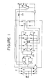
- the inverter circuit which is employed in such welding power supply generally has transistors 11 to 14 connected bridge-like between output terminals of a rectifier circuit 7 with diodes 1 to 6 and turned on and off by the output signal of a drive circuit 20 in the manner as described hereinbelow, thereby to produce an alternate current in its output transformer 21.
- the output of the transformer 21 is rectified through a rectifier circuit 22 and applied to a welding electrode 24 through a reactor 23 to generate an arc across the welding electrode 24 and a base metal 24' thereby to perform a predetermined welding operation.
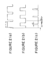
- the welding voltage and welding current are controlled by varying the conduction period t of the transistors 11 to 14 as shown particularly in FIGURE 2, depicting output waveforms as obtained by using-a resistance load without a DC reactor, namely at (a) a waveform at the maximum output, at (b) a waveform at an output level of 1/2 the maximum output, and at (c) a waveform at an output level of 1/5 the maximum output.
- the pulse width t is narrowed in a low welding current range, inviting deteriorations in the welding characteristics due to an increased ripple content in the output voltage.
- the ripple content of the output voltage can be minimized by increasing the reactance of the reactor 23, it is desired to hold the reactance of the reactor 23 as small as possible since a higher impedance of the reactor 23 will augment the delay of response and lower the efficiency.
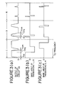
- FIGURE 3 in which there are shown at (I) to (III) one-period waveforms at high, medium and low load currents, respectively. Shown at (a) of FIGURE 3 is the output waveform of the rectifier circuit 22, at (b) the base input of the transistors 11 and 13, and at (c) the base input of transistors 12 and 14.
- t on indicates the turn-on time of the transistors 11 to 14, toff their turn-off time, and t st g their storage time.
- the ripple component can be reduced by increasing the reactance of the reactor but it will lower the response and efficiency as mentioned hereinbefore.
- the rates of t on toff and t st g at 1/2 periods can be reduced by lowering the inverter frequency, thereby to stabilize the low output current and voltage. However, it will increase the weights of the transformer and reactor contrary to the initial objective of minimizing the transformer and reactor by heightening the inverter frequency.
- the welding power supply of this sort is required to be capable of stabilizing the welding characteristics over large and small current ranges.
- a welding power source of 500 A should not show a material drop in welding characteristics at a 1/3 output level, namely at 170 A.
- the power supply is required to be able to control the current and voltage with high response and at a suitable time point in a final stage of each short circuit perid.d of large current since otherwise intense spattering occurs by explosive rupturing of the short circuit.
- the present invention aims to eliminate or at least mitigate the above-mentioned various drawbacks or difficulties of the conventional welding power supply systems.
- a DC power supply system for consumable or non-consumable electrode welding comprising: a plurality of inverter units adapted to convert a first direct current into an alternate current and to rectify the alternate current to produce an output of a second direct current; a circuit connecting the output terminals of said inverter units in parallel relation; a detection circuit for detecting the total output current of said inverter units; and a circuit for varying the number of operating inverter units according to the value of the detected total output current.
- the power supply system is further provided with a phase control means for controlling the phases of alternate currents produced by the respective inverter units, or means for selectively actuating a particular inverter unit or units in a short circuit period of large current in dip transfer welding, or feedback means for suppressing the current in a controlled timing in the final stage of each short circuit period to prevent spattering as caused by bursting rupture of the large short circuit current.
- a phase control means for controlling the phases of alternate currents produced by the respective inverter units, or means for selectively actuating a particular inverter unit or units in a short circuit period of large current in dip transfer welding, or feedback means for suppressing the current in a controlled timing in the final stage of each short circuit period to prevent spattering as caused by bursting rupture of the large short circuit current.
- the present invention also provides a power supply system for dip transfer welding with a consumable electrode, said power supply system comprising: a first inverter unit adapted to generate a voltage suitable for arcing periods; a second inverter unit connected in parallel with said first inverter unit and adapted to generate a voltage suitable for short circuit periods; a first control circuit for controlling the voltage and current of said first inverter unit; a second control circuit for controlling the current of said second inverter unit; the output of said first inverter unit being fed to said consumable electrode in arcing periods, and the output of said second inverter unit being fed to said consumable electrode in short circuit periods along with the output of said second inverter unit.
- the present invention further provides a power supply system for use in dip transfer welding in which a short circuit period and an arcing period alternately take place, said power supply system comprising: a voltage detector for detecting the output voltage of said power supply system; a memory for reading and storing the lowest output voltage of said power supply system in each short circuit period; a trigger circuit for triggering reading and erasing operations of said memory; a level indicator; a comparator adapted to produce an output signal when the difference between the output voltage detected by said voltage detector and the lowest output voltage stored.in said memory is greater than the output signal of said level indicator; a final-stage short circuit current indexer; and a welding power output for producing a current of a value specified by said final-stage short circuit current indicator in response to a signal from sai.d.comparator.
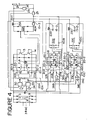
- FIGURE 4 there is shown a DC welding power supply system, in which designated by reference numerals lOA to 10C are high frequency inverter units each including transistors 11 to 14 which are bridged in the same manner as in FIGURE 1, a pulse width control 20A, 20B or 20C, base drive circuits 20-1 to 20-4 for the respective transistors, an output transformer 21A, 21B or 21C, and a rectification circuit 22A, 22B or 22C.
- the inverter units lOA to 10C are connected to a DC output terminal of a rectification circuit 7 which diodes 1 to 6 to apply a predetermined DC voltage across the collector of transistor 11 and the emitter of transistor 12 and across the collector of transistor 13 and the emitter of the transistor 14 of the respective inverter units lOA to lOC.
- the inverter units lOA to 10C have the respective positive (+) output terminals 15-1 connected commonly and have their negative (-) output terminals 15-2 connected commonly to the source side of a current detector 25.
- the output terminals of the respective inverter units 10A to 10C are connected parallel with each other.
- a voltage detector 26 which detects the output voltage of the power supply, a welding electrode 24 and a base material 24'.
- Designated at 30 is an error amplifier for voltage control, which is differentially applied with a preset voltage signal supplied from a voltage indexer 31 and with the output signal of the voltage detector 26 indicating the output voltage of the power supply to produce a voltage signal proportional to the difference between the two input signals.
- the output terminal of the error amplifier 30 is connected to the input terminals of the pulse width controls 20A to 20C of the respective inverter units lOA to 10C through diodes 32A to 32C, respectively.
- the pulse width controls 20A to 20C of the inverter units lOA to 10C are commonly supplied with the output signal of the error amplifier 30.
- the reference numeral 33 denotes an error amplifier for current control, which is differentially applied with a signal of the present current from the current selector 34 and with the output signal of the current detector 25 indicating the output current of the power supply, to produce an output signal according to the differences between the input signals.
- the output terminal of the current error amplifier 33 is connected to the pulse width controls 20A to 20C of the inverter units lOA to 10C through diodes 35A to 35C respectively.
- the pulse width controls 20A to 20C are thus commonly supplied with the output of the error amplifier 33.
- the inverter units lOB and lOC are actuated or deactuated by comparators 36B and 36C according to the level of load current, the comparators 36B and 36C being connected to the pulse width controls 20B and 20C through diodes 37B and 37C, respectively.
- the comparators 36B and 36C have one input terminals thereof connected to the current detector 25 and the other input terminals to the current indexer 38B and 38C, respectively.
- the current indexer 38B is preset, for example, at a current level (1/3-a) slightly smaller than 1/3 of the maximum output current I 0 of the welding power supply, so that the comparator 36B produces an output of "1" if the welding current is higher than the preset value to actuate the inverter unit lOB.
- the comparator 36B produces an output of "0" to de-actuate the inverter unit lOB.
- the current indexer 38C is preset, for example, at a current level (2/3-a) slightly lower than 2/3 of the maximum output current I 0 of the welding power supply, and actuates or de-actuates the inverter unit 10C depending on whether or not the welding current is greater than the preset value.
- the inverter units 10A to 10C are provided with current detectors 40A to 40C, respectively, to control the current of the corresponding inverter unit by a circuit (not shown) when its output current exceeds a predetermined rated value.
- the comparators 36B and 36C produce output signals of "1" to hold the inverter units lOA to 10C all in actuated state. Consequently, the transistors 11 to 14 of the inverter units lOA to 10C are turned on and off in a predetermined timing according to the output signals of the base drive circuits 20-1 to 20-4, producing a high frequency output at the output transformers 21A to 21C.
- the output currents of the transformers 21A to 21C are rectified through the rectification circuits 22A to 22C, respectively, and applied to the welding electrode 24 through reactors 23A to 23C to produce a predetermined arc for welding the base material 24 1 .
- the sum of the output currents of the inverter units lOA to lOC flows through the welding electrode 24.
- the output voltage of the welding power supply is detected by the voltage detector 26, and the value of the detected voltage is applied to the voltage error detector 30 which produces an output signal according to the difference from the preset value specified by the voltage indexer 31.
- This output signal is applied to the pulse width controls 20A to 20C through diodes 32A to 32C; respectively, to control their output pulse width and thus the conduction angle of the transistors 11 to 14, maintaining the output voltage of the inverter units lOA to lOC at the preset value.
- the current detector 25 which detects the welding current supplies a signal of the detected current to the current error amplifier 33 which in turn produces an output signal according to the difference from the value of preset value specified by the current indexer 34.
- This output signal is applied to the pulse width controls 20A to 20C of the inverter units lOA to 10C through diodes 35A to 35C, respectively, to control their output pulse width.
- the conduction angle of the transistors 11 to 14 are controlled to maintain the welding current at the preset value.
- the comparator 36C and the pulse width control 20C produces output signals of "O", de-actuating the inverter unit 10C as shown at C of FIGURE 7.
- the output signal of comparator 36B is at "1" so that the inverter unit lOB is put in operation to produce a predetermined output as shown at A and B of FIGURE 7. Therefore, in this case the sum of the output signals of the inverter units lOA and lOB is applied to the welding electrode as shown in FIGURE 8.
- the comparators 36B and 36C both produce an output signal of "O" as shown at B and C of FIGURE 9 to de-actuate the inverter units lOB and 10C, performing the welding operation solely by the output of the inverter unit 10A.
- the width of the space S' of the output waveform is broadened even with a load greater than 1/3 of the maximum output, as shown in FIGURES 13 to 15, increasing the content of the ripple component.
- a power supply with a maximum output of 400 A can ensure a stable welding operation even at a small output current, for example, at about 60 A.
- the space S" of the output waveform of the inverter is extremely broadened at an output level of about 1/9 of the maximum output as shown particularly in FIGURE 16, increasing the ripple content to such an extent as will be practically unacceptable.
- inverter units Although three inverter units are employed in the foregoing embodiment, it is possible to employ a combination of an arbitrary number of inverter units in the power supply according to the present invention.
- the reactance of the reactor in the output circuit can be lowered, permitting to prevent deteriorations in response characteristics which would otherwise be caused by the reactance.
- a welding power supply of high response which can comply with higher requirements in the welding operations.
- the inverter units which employ universal type switching elements of small size as compared with the maximum output can be constructed at a low cost.
- the power supply of the present invention is particularly suitable for use in the short arc welding in which a period of short circuit and a period of arc generation alternately take place and which involves large current variations from 130 A of the arcing period to 400 A of the short circuit period although the average current is 150 A, requiring the output current of a power supply to follow such large current variations.
- the embodiment of FIGURE 4 can comply with such a requirement all by the electric circuits arrangements with a high response.
- the switching elements like transistors of the inverters are also burned on for a longer time period as compared with their time characteristics including turn-off time t off' conduction time t on and storage time tstg, preventing an accurate control from being impaired by the various time characteristics.
- the welding electrode in the foregoing embodiment may be either a consumable type or a non-consumable type. If desired, arrangement may be made such that a group or groups of a plural number of inverter units are actuated and de-actuated according to the load current.
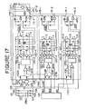
- FIGURE 17 there is shown another embodiment of the present invention, which is basically the same as the foregoing embodiment except for the provision of a phase control means for controlling the phase angles of alternate waves produced by the respective inverter units and wherein designated at 110A to 110C are high frequency inverter units each including transistors 111 to 114 which are bridged in the same manner as in FIGURE 1, a pulse width selector 120A, 120B or 120C, base drive circuit 120-1 to 120-4 for the respective transistors, an output transformer 121A, 121B or 121C, and a rectification circuit 122A, 122B or 122C.
- 110A to 110C are high frequency inverter units each including transistors 111 to 114 which are bridged in the same manner as in FIGURE 1, a pulse width selector 120A, 120B or 120C, base drive circuit 120-1 to 120-4 for the respective transistors, an output transformer 121A, 121B or 121C, and a rectification circuit 122A, 122B or 122C.
- the inverter units 110A to 110C are connected to the DC output terminals of a rectification circuit 107 with diodes 101 to 106 to apply a predetermined DC voltage across the collector of transistor 111 and the emitter of transistor 112 and across the collector of transistor 113 and the emitter of the transistor 114 of the respective inverter units 110A to 110C.
- the inverter units 110A to 110C have the respective positive (+) output terminals 115-1 connected commonly and have their negative (-) output terminals 115-2 connected commonly to the source side of a current detector 125.
- the output terminals of the respective inverter units 110A to llOC are connected parallel with each other.
- a voltage detector 126 which detects the output voltage of the power supply, a welding electrode 124 and a work 124'.
- Designated at 130 is an error amplifier for voltage control, which is differentially applied with a preset voltage signal supplied from the voltage indexer 131 and with the output signal of the voltage detector 126 indicating the output voltage of the power supply, to produce a voltage signal according to the difference between the input signals.
- the output terminal of the error amplifier 130 is connected to one input terminals of the comparators 133A to 133C of the inverter units 110A to 110C through diodes 132A to 132C, respectively.
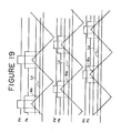
- Applied to the other input terminals of the comparators 133A to 133C are 20 kHz saw-tooth waves, WA, WB and WC of 20 kHz which are fed from a saw-tooth wave generator 134 with a delay of a 1/3 period as shown in FIGURE 18.
- the comparators 133A to 133C each produce an output signal of "1" when the signal applied to one input terminal becomes smaller than the triangular wave fed from a triangular wave generator 134.
- the output terminals of the comparators 133A to 133C are connected to frequency dividers 120A'.to 120C of the respective inverter units 110A to 110C.
- the frequency dividers 120A to 120C divide into two phases the pulses produced by the comparators 133A to 133C, respectively, for application to base drive circuits 120-1 to 120-4.
- Indicated at 135 is an error amplifier for the current control, which is differentially applied with a signal of a preset current from the current indexer 136 and a signal from the current detector 125 indicating the output current of the power supply, to produce an output signal according to the difference between the two input signals.
- the output terminal of the current error amplifier 135 is connected to the other input terminals of the comparators 133A to 133C of the inverter units 110A to 110C through diodes 137A to 137C, respectively.
- the afore-mentioned diode 132A and diode 137A constitute a diode OR circuit (logical sum circuit) which applies to the comparator 133A a higher one of the signals from the error amplifiers 130 and 135, so that the power supply produces an output which satisfies either one of the values specified by the preset current indexers 131 and 136.
- the output of the triangular wave generator 134 has a phase difference of a 1/n period if the power supply is provided with an n-number of inverter units. It is also possible to impart a phase lag of a 2/n period by the use of n/2 triangular wave generators.
- the difference between the preset voltage specified by the preset voltage indexer 131 and the actual output voltage detected by the voltage detector 126 is amplified by the error amplifier 130 and applied to the comparators 133A to 133C through diodes 132A to 132C, respectively.
- the comparators 133A to 133C produce output pulses P A to P C , respectively, in a range where the triangular wave exceeds the level L 1 .
- the generation of the pulses P A to P c is asynchronized according to the phase lag of the triangular waves W A to W C .
- the output pulses of the comparators P A to P C of the comparators 133A to 133C are applied to the frequency dividers 120A to 120C and thereby divided into two phase pulses and applied to the transistors 111 to 114 through the corresponding base drive circuits 120-1 to 120-4 of the inverter unit 110A, 110B or 110C.
- the transistors 111 and 114 are simultaneously turned on and off for a predetermined time period alternately with the transistors 112 and 113 to produce in the transformers 121A to 121C alternate currents of, for example, 10 kHz with a phase lag of 120°. These alternate currents are rectified through rectification circuits 122A to 122C, respectively.
- the outputs of the inverter units 110A to 110C appear at their output terminals with a phase lag corresponding to that of the triangular waves W A to W C , so that the output which is obtained at the output terminals 127-1 and 127-2 of the power supply has a waveform with a lessened ripple component.
- the output voltage of the error amplifier 130 corresponds to the deviation from the preset value of the detected voltage, the output voltage of the power supply is maintained at the preset value.
- the value of the output current which is detected by the current detector 125 is applied to the error amplifier 135 which produces an output voltage proportional to the difference of the detected current from the preset value of the current indexer 136.
- the output voltage of the error amplifier 135 is fed to the comparators 133A to 133C through diodes 137A to 137C, respectively.
- the frequency divider 120A to 120C are controlled in a manner similar to the above-described voltage control, thereby controlling the conduction angles of the transistors of the inverters 110A to 110C to maintain the output current at the present value.
- the currents of the inverter units 110A to 110C are detected by the current detectors 140A to 140C, respectively, and restricted to a level below a predetermined value by a current limiting circuit which is not shown.
- the output pulses of the comparators 133A to 133C are narrowed as shown at P A l to P C '.
- direct currents corresponding to the pulses P A l to P C ' are successively applied across the output terminals 127-1 and 127-2 of the welding power supply, suppressing the increase of the ripple component at the output terminals.
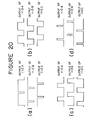
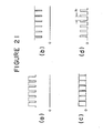
- FIGURE 20 Shown in FIGURE 20 are the output waveforms of the inverter units 110A to 110C and in FIGURE 21 the waveforms of the total output of the three inverter units, with regard to (a) the maximum output, (b) 2/3 the maximum output, (c) 1/3 the maximum output and (d) 1/9 the maximum output.
- the respective output waves are shown in square forms,
- a total output of the power supply according to the invention has a waveform with smaller intervals, with reduced ripple component.
- the output waveform of the power supply according to the present invention has a smaller pulse interval X 1 as compared with the interval of the conventional counterpart, and consists of waves of a smaller amplitude with a ripple component which is small enough to permit practical applications.
- the power supply of the foregoing embodiment can also ensure stable welding operations at a small output current of, for example, about 90 A even in a case where the maximum output is 500 A.
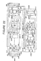
- FIGURE 22 there is shown another welding power supply according to the present invention, which is provided with a couple of inverter type DC power sources to be selectively operated for short circuiting an arc generating periods in dip transfer welding for reducing the capacity (KVA) of the power supply in addition to the reductions in size and weight.
- KVA capacity
- the reference numerals 210A and 210B denote high frequency inverter units including transistors 211 to 214 which are bridged in the same manner as in FIGURE 1, pulse width selectors 220A and 220B, base drive circuits 220-1 to 220-4 for the respective transistors, output transformers 221A and 221B, and rectification circuits 222A and 222B.
- the inverter units 210A and 210B are connected to DC output terminals of a rectification circuit 207 with diodes 201 to 206 for rectifying mains three-phase AC current, supplying a predetermined DC voltage across the collector and emitter of the transistors 211 and 212 and across the collector and emitter of the transistors 213 and 214 of the respective inverter units 210A and 210B.
- the winding ratios of the output transformers 221A and 221B of the inverter units 210A and 210B are determined such that the former has a maximum output of 30V-250A and the latter a maximum output of 10V-250A.
- the positive (+) output terminals 215-1 of the inverter units 210A and 210B are commonly connected to an output terminal 218, having their negative (-) output terminals 215-2 connected also commonly to the source side terminal of a current detector 225.
- the output of the two inverter units 210A and 210B are connected parallel with each other.
- a voltage detector 226 which detects the output voltage of the power supply system, a welding electrode 224 and a base material 224'.
- Indicated at 230 is an error amplifier for controlling the voltage of the inverter unit 210A, which is differentially applied with a signal of the preset voltage from the voltage indexer 231 and a signal of the detected voltage from the voltage detector 226 indicating the actual output voltage of the power supply system, producing an output signal of a voltage corresponding to the difference between the two input signals.
- the output terminal of the error amplifier 230 is connected to a pulse width control 220A of the inverter unit 210A through diode 232.
- the reference numeral 233 denotes an error amplifier which controls the inverter unit 210A to hold the total output currents of the inverter units 210A and 210B at a predetermined value, and which is differentially applied with a signal of a preset current value from a current indexer 235 and a signal of the total output current of the power system from the current detector 225, producing an output signal according to the difference between the two input signals.
- the output terminal of the current control error amplifier 233 is connected to the input terminal of the pulse width control 220A through diode 234.
- the output signals of the error amplifiers 230 and 233 are thus applied to the pulse width control 220A through parallel circuits of diodes 232 and 234, so that the pulse width control 220A produces output pulses of a width corresponding to the logical sum of the output of the two error amplifiers 230 and 233.
- the reference numeral 225 denotes a current detector solely for the inverter 210A.
- the inverter unit 210B is provided with an error amplifier 240 for controlling the current at: a value lower than its maximum output current, the error amplifier 240 being supplied with a signal of a preset current from the current indexer 241 and a signal of detected current from the current detector 242 in the output circuit of the inverter unit 210B, to produce an output signal to be fed to the pulse width setter 220B to control the output current of the inverter unit 210B below a preset value.
- Indicated at 243 is an error amplifier which controls the inverter units 210B such that the total output current of the two inverter units 210A and 210B takes a predetermined value, and which is differentially applied with a signal of preset current from the current indexer 244 and a signal of detected welding current from the current detector 225 indicating the total ouput current of the power supply system, to produce an output signal proportional to the difference between the two input signals.
- the output terminal of the error amplifier 243 is connected to the pulse width control 220B through diode 245-1.
- Denoted at 246 is a comparator which control the inverter units 210B to actuate and de-actuate same in short circuit and arcing periods of the welding operation, respectively.
- the comparator 246 is supplied compares the signal of preset voltage from the voltage indexer 247 with the signal of detected actual voltage from the voltage detector 226 to produce an output signal of "0" when the detected voltage is higher than the preset value and otherwise an output signal of "1".
- the output terminal of the comparator 246 is connected to the pulse width control 220B, which produces an output signal to actuate the inverter unit 210B when the output of the comparator 246 is "1" and an output signal to de-actuating the inverter unit 210B when the output of the comparator 246 is "O".
- the current indexer 241 is preset, say, at 250A while the voltage indexer 247 is preset, say, at 12V.
- the comparator 246 produces an output signal of "O" to hold the inverter unit 210B in de-actuated state.
- the inverter unit 210A alone is operated in the arcing period in the following manner.
- the DC voltage for example, a DC voltage of 280V which is obtained from the rectification circuit 207 is applied to the transistors 211 to 214.
- the signal indicating the terminal voltage detected by the voltage detector 226 is applied to the error amplifier 230, which produces an output signal according to the deviation from the signal of preset voltage supplied from the voltage indexer 231, feeding the output signal to the pulse width control 220A.
- the load current which is detected by the current detector 225 is fed to the error amplifier 233, which produces an output signal according to the deviation from the signal of preset value from the current indexer 235, applying the output signal to the pulse width control 220A.
- the pulse width control 220A produces pulses of a width corresponding to the logical sum of the outputs of the error amplifiers 233 and 230 thereby to drive the transistors 211 to 214.
- the comparator 246 of the inverter unit 210B produces an output signal of "1" to actuate the pulse width control 220B. Therefore, the inverter units 210A and 210B are operated concurrently to supply the sum of the output currents to the two inverter units 210A and 210B to the welding electrode 224.
- the total output current of the inverter units 210A and 210B which is detected by the current detector 225, is applied to the error amplifier 233 of the inverter unit 210A as well as to the error amplifier 243 of the inverter unit 210B, each error amplifier producing an output signal corresponding to the deviation of the input signal.
- the pulse width controls 220A and 220B produce pulses of corresponding widths thereby driving the transistors 211 to 214 at predetermined conduction angles to maintain the output currents of the inverter units 210A and 210B at predetermined values, for example, at 250A for both inverter units 210A and 210B in this particular example.
- substantially the inverter unit 210A alone is driven in an arcing period to produce an output of 30V-250A, while in a short circuiting period both inverter units 210A and 210B are driven to produce an output of 10V-500A in total, adding the output of 10V-250A by the inverter unit 210B.
- the error amplifier 240 produces an output which controls the pulse width modulator 220B in such a manner as to clamp the output of the inverter unit 210B at 250A.
- this circuit including the current detector 242 and error amplifier 240, is not necessarily required.
- the voltage indexer 247 and comparator 246 may also be omitted if desired. If they are omitted, the inverter unit 210B produces an output of 10V in an arcing period of 23V-200A, but there occurs no current flow from the inverter unit 210B since the arc voltage is, say,at 23V.
- the voltage in the arcing period can be adjusted by altering the preset value of the voltage indexer 231 of the inverter unit 210A, while the short circuiting current in the short period is adjustable by altering the preset value of the current indexer 244 of the inverter unit 210B. It should be noted that the output voltage and current of the respective inverter units can also be arbitrarily determined. If desired, arrangement may be made to operate simultaneously a plural number of parallel inverter units.
- the power supply is required to have a response at least ten times as high as the short circuiting time of 1 ms - 5 ms, namely, to be able to make at least one feedback per 100 ps.
- the frequency of the inverter is preferred to be as high as possible to suppress the phenomenon of short circuit welding.
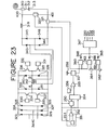
- FIGURE 23 shows a further embodiment which is provided with a feedback control to suppress the current with a good timing in a final stage of short circuit periods of large current, which have a great influence on spattering.
- the transformer 342 has such a winding ratio as to produce on its secondary side a voltage suitable for welding.
- the diodes 338 to 341 conduct when the primary winding of the transformer 342 becomes higher than the input voltage, serving to clamp it below the input voltage and at the same time to feed back the stored energy of the primary winding of the transformer to the input power source when the transistors 334 to 337 are turned off.
- the output of the secondary side of the transformer 342 is rectified again by diodes 343 to 346 and supplied to a contact tip 310 through a reactor 319. Power is supplied as a wire 311 is passed through the contact tip 310, generating an arc across the wire 311 and a base material 313.
- the reactor 319 may be omitted in some case.
- the current or voltage across the output terminals 400 and 401 of the inverter is adjustable by varying the ratio of the turn-on time to the turn-off time of the transistors 334 to 337.
- the reference numerals 320 and 321 denote a voltage detector and a current detector, respectively.
- the voltage detector 320 which is connected to the output terminals 400 and 401 produces an output signal of detected voltage, corresponding to the voltage applied across the output terminals 400 and 401.
- the output terminal of the voltage detector 320 is connected to one input terminal of an error amplifier 361 which controls the output voltage across the terminals 400 and 401 in the arcing periods.
- the other input terminal of the error amplifier 361 is connected to an arc voltage indexer 362.
- the current detector 321 produces an output signal proportional to the output current of the power supply system, and its output terminal is connected to one input terminal of an error amplifier 363 which controls the output current.
- the other input terminal of the error amplifier 363 is connected to a short circuit current indexer 364.
- the output terminals of the error amplifiers 361 and 363 are connected to a pulse width control 367 through diodes 365 and 366, respectively.
- the voltage in an arcing period which is indicated by the output signal of the voltage detector 320 is compared with the signal from the voltage indexer 362 by the error amplifier 361, which produces an output signal proportional to the deviation of the detected voltage.
- This output signal is fed through diode 365 to the pulse width control 367 which produces a pulse width signal determined in accordance with the value of deviation, supplying the pulse width signal alternately to the base drive circuits 330 and 331 and the other base drive circuits 332 and 333.
- the transistors 334 and 335 and the transistors 336 and 337 are alternately turned on by the base drive circuits 330 to 333 for a time length corresponding to the pulse width, thereby controlling the output voltage of the power supply system at a value determined by the voltage indexer 362.
- the signals of the current detector 321 and the short circuit current indexer 364 are compared and amplified by the error amplifier 363, supplying an error signal to the pulse width indexer 363 through diode 366 thereby to control the output current of the power supply system to a value specified by the short circuit current indexer 364 in the same manner as in the above-described voltage control.
- the output terminal of the voltage detector 320 is connected to a memory 350 which stores the lowest voltage applied across the welding wire 311 and the work 313, as well as to one input terminal of a comparator 352 of a trigger circuit 351 which controls the operation of the memory 350.
- a voltage indexer 353 Connected to the other input terminal of the comparator 352 is a voltage indexer 353 which produces a signal of a reference voltage intermediate between the arc voltage and the short circuit voltage.
- the output terminal of the comparator 352 is connected to the memory 350 and produces an output signal of "1" when the detected voltage is lower than the preset voltage thereby to actuate the memory 350 to store the minimum value of the terminal voltage detected by the voltage detector 320.
- the output terminal of the memory 350 is connected to one input terminal of a subtractor 354 which has the other input terminal connected to the output terminal of the voltage detecton 320 to compute the difference V between the minimum voltage stored in the memory 350 and the terminal voltage.
- the output terminal of the subtractor 354 is connected to one input terminal of a comparator 355 which has the other input terminal connected to a level indexer 356, with its output terminal connected to an analog switch 357.
- the analog switch 357 has its input terminal connected to a final-stage short circuit current detector 358 and its output terminal to an error amplifier 360 for lowering the short circuit current.
- the trigger circuit 351 actuates the memory 350 to start reading.
- the memory 350 stores the minimum value of the signal from the voltage detector 320, namely, the minimum voltage across the output terminals 400 and 401.
- the subtractor 354 produces an output signal indicating the difference between the signals of the voltage detector 320 and memory 350.
- the comparator 355 turns on the analog switch 357 to feed the signal of the final-stage short circuit current indexer 358 to the error amplifier 360 thereby to compare and amplify the difference between the signals of the final-stage short circuit current indexer 358 and the current detector 321 and controlling the output current of the power supply system to the value specified by the final-stage short circuit current indexer 358.
- the analog switch 353 is off, the error amplifier 3.60 is controlled by a preset current value higher than that of the short circuit current command 364 or a non-limiting signal although not shown.
- the diodes 365, 366 and 368 constitute the so- called diode OR circuit so that a pulse width which satisfies either one of the conditions stipulated by the error amplifiers 360, 361-and 363 is established in the pulse width command 367.
- the output in the arcing period is about 23V-180A and the analog switch 357 is off at this time, imposing no limit on the current. Therefore, although the error amplifiers 360, 361 and 363 instruct the power supply system to produce an output of oo A, 400A and 23V, respectively, the power supply system produces an output of 23V which is satisfied by the diode OR circuit.
- the analog switch 357 is not yet turned on by the output of the comparator 355 after occurrence of short circuiting between the welding wire 311 and work 313, the error amplifiers 360, 361 and 363 still call for the outputs of oo A, 400A and 23V, respectively. Therefore, the power supply system tends to produce an output of 32V, but the load current is increased due to a reduction of load impedance caused by short circuiting and current of 400A flows through the load.
- the preset current of 400A of the short circuit current indexer 364 satisfies a value specified by the error amplifier 360, 361 and 363, so that the power supply system produce an output of 400A regardless of the voltage.
- the supply voltage in a short circuit period is applied to the comparator 352 through the voltage detector 320 for comparison with the preset voltage of the reference voltage indexer 353, the comparator 352 sending the memory 350 a command signal to start reading the minimum voltage when the voltage of the power supply becomes lower than the preset value.
- the memory 350 stores the lowest value V of the detected voltage from the voltage detector 320..
- the subtractor 354 computes the difference of the lowest value V stored in the memory 350 from the output V of the voltage detector 320, turning on the analog switch 357 if the difference is greater than the preset value of the level indexer 356 to feed the final-stage short circuit current indexer 358 to the error amplifier 360 through the analog switch 357.
- the output of the power supply is determined in preference of the output of the error amplifier 360 which is governed by the signal of preset current 200A from the final-stage short circuit current indexer 358, lowering the output current from 400A to 200A. In this manner, the output current in the final stage of the short circuit period in transition to an arcing period is lowered to a value as low as 200A to suppress spattering.
- a trigger circuit 351 which is constructed as shown in FIGURE 24.
- the trigger circuit includes a comparator 372 which produces an output signal when the signal of the voltage detector 320 is smaller than a signal of a voltage indexer 371 which produces a signal of a voltage intermediate between the short circuit voltage and the arc voltage; a comparator 374 which produces an output signal when the signal of the current detector 321 becomes the same as or greater than the signal of a voltage indexer 373 which produces a signal corresponding to or slightly smaller than the short circuit current; and a logic circuit 375 which instructs the memory 350 to start reading when the comparators 372 and 374 simultaneously produce output signals and to erase the memory when the output signal of the comparator 372 disappears.
- this trigger circuit 351 the reading is not started until the current reaches the value of short circuit current in each short circuit period, and the memory is erased upon generation of an arc.
- the level indexer 356 is arranged as shown at 380 of FIGURE 25. Namely, the output of the current detector 321 is fed to the comparator 355 after shaping waves through a filter circuit 381 and multiplying a constant k by a multiplier 382.
- the filter circuit 381 may be omitted if the current has a smooth waveform.
Landscapes
- Engineering & Computer Science (AREA)
- Physics & Mathematics (AREA)
- Plasma & Fusion (AREA)
- Mechanical Engineering (AREA)
- Arc Welding Control (AREA)
Applications Claiming Priority (8)
| Application Number | Priority Date | Filing Date | Title |
|---|---|---|---|
| JP127972/81 | 1981-08-13 | ||
| JP127971/81 | 1981-08-13 | ||
| JP12797281A JPS5829573A (ja) | 1981-08-13 | 1981-08-13 | 直流溶接用電源装置 |
| JP127974/81 | 1981-08-13 | ||
| JP127973/81 | 1981-08-13 | ||
| JP12797481A JPS5829575A (ja) | 1981-08-13 | 1981-08-13 | 溶接用電源装置 |
| JP56127971A JPS5829572A (ja) | 1981-08-13 | 1981-08-13 | 直流溶接用電源装置 |
| JP12797381A JPS5829574A (ja) | 1981-08-13 | 1981-08-13 | 短絡移行溶接用電源装置 |
Publications (2)
| Publication Number | Publication Date |
|---|---|
| EP0072683A2 true EP0072683A2 (fr) | 1983-02-23 |
| EP0072683A3 EP0072683A3 (fr) | 1983-09-21 |
Family
ID=27471349
Family Applications (1)
| Application Number | Title | Priority Date | Filing Date |
|---|---|---|---|
| EP82304288A Withdrawn EP0072683A3 (fr) | 1981-08-13 | 1982-08-13 | Dispositif d'alimentation à courant continu pour soudage |
Country Status (2)
| Country | Link |
|---|---|
| US (1) | US4503316A (fr) |
| EP (1) | EP0072683A3 (fr) |
Cited By (11)
| Publication number | Priority date | Publication date | Assignee | Title |
|---|---|---|---|---|
| DE3816238A1 (de) * | 1987-05-12 | 1988-12-01 | Kobe Steel Ltd | Stromversorgungssystem zur abschmelzelektroden-lichtbogenschweissung und verfahren zum steuern desselben |
| DE3804387C1 (en) * | 1988-02-12 | 1989-08-24 | B & V Beschichten Und Verbinden Gmbh, 6800 Mannheim, De | Arc welding device having an extended drive range |
| FR2638992A1 (fr) * | 1988-11-17 | 1990-05-18 | Honda Motor Co Ltd | Appareil de soudage par resistance en courant continu |
| EP0382110A3 (en) * | 1989-02-06 | 1990-09-19 | The Lincoln Electric Company | Output control circuit for reversers, and high-frequency power supply for the dc supply of a welding station |
| EP0435673A3 (en) * | 1989-12-28 | 1992-02-19 | Daihen Corporation | Power source apparatus for alternating-current arc welding, capable of supplying an alternating-current welding current having any waveform |
| US5196668A (en) * | 1988-11-17 | 1993-03-23 | Honda Giken Kogyo Kabushiki Kaisha | DC resistance welding apparatus |
| US5229567A (en) * | 1988-11-17 | 1993-07-20 | Honda Giken Kogyo Kabushiki Kaisha | Switching control system for controlling an inverter of a spot resistance welding apparatus |
| GB2309130A (en) * | 1996-01-11 | 1997-07-16 | Illinois Tool Works | Arc welding; switch mode power supply |
| GB2320110A (en) * | 1996-01-11 | 1998-06-10 | Illinois Tool Works | Switch mode power supply; arc welding |
| US6107602A (en) * | 1996-01-11 | 2000-08-22 | Illinois Tool Works Inc. | Switchable power supply with electronically controlled output curve and adaptive hot start |
| AU772634B2 (en) * | 2000-01-27 | 2004-05-06 | Crc For Welded Structures Limited | A welding control system |
Families Citing this family (29)
| Publication number | Priority date | Publication date | Assignee | Title |
|---|---|---|---|---|
| SE438109B (sv) * | 1983-11-28 | 1985-04-01 | Esab Ab | Stromkella for ljusbagsvetsning |
| US4763237A (en) * | 1986-10-17 | 1988-08-09 | Wieczorek John P | DC/AC/DC Power conversion system including parallel transformers |
| US4823250A (en) * | 1987-11-05 | 1989-04-18 | Picker International, Inc. | Electronic control for light weight, portable x-ray system |
| JPH0728555B2 (ja) * | 1989-06-02 | 1995-03-29 | 三菱電機株式会社 | 可変速駆動装置 |
| US4916599A (en) * | 1989-03-29 | 1990-04-10 | Hyperpower, Inc. | Switching power supply |
| IT1242893B (it) * | 1990-12-27 | 1994-05-18 | Cefin Spa | Dispositivo elettronico per la gestione ed il controllo dell'energia elettrica di alimentazione per saldatura a resistenza, in particolare di corpi di scatole metalliche. |
| US5349157A (en) * | 1993-01-04 | 1994-09-20 | The Lincoln Electric Company | Inverter power supply for welding |
| JP3234909B2 (ja) * | 1996-12-13 | 2001-12-04 | シャープ株式会社 | インバータ制御装置、およびインバータの制御方法 |
| JP3231705B2 (ja) * | 1998-07-08 | 2001-11-26 | 株式会社三社電機製作所 | アーク加工用電源装置 |
| US6215086B1 (en) | 1998-12-24 | 2001-04-10 | Welding/Technology Corp. | Resistance welding controller |
| US6291798B1 (en) * | 1999-09-27 | 2001-09-18 | Lincoln Global, Inc. | Electric ARC welder with a plurality of power supplies |
| AT412076B (de) * | 2000-12-15 | 2004-09-27 | Fronius Schweissmasch Prod | Verfahren zum verbinden mehrerer schweissgeräte sowie schweissgerät hierfür |
| AU2006200414B2 (en) * | 2001-04-17 | 2009-11-19 | Lincoln Global, Inc. | Electric arc welding system |
| US6472634B1 (en) * | 2001-04-17 | 2002-10-29 | Lincoln Global, Inc. | Electric arc welding system |
| US6713721B2 (en) * | 2001-09-19 | 2004-03-30 | Illinois Tool Works Inc. | Method of designing and manufacturing welding-type power supplies |
| US8269141B2 (en) * | 2004-07-13 | 2012-09-18 | Lincoln Global, Inc. | Power source for electric arc welding |
| US8785816B2 (en) | 2004-07-13 | 2014-07-22 | Lincoln Global, Inc. | Three stage power source for electric arc welding |
| US9956639B2 (en) | 2005-02-07 | 2018-05-01 | Lincoln Global, Inc | Modular power source for electric ARC welding and output chopper |
| US8581147B2 (en) * | 2005-03-24 | 2013-11-12 | Lincoln Global, Inc. | Three stage power source for electric ARC welding |
| US9855620B2 (en) | 2005-02-07 | 2018-01-02 | Lincoln Global, Inc. | Welding system and method of welding |
| US9647555B2 (en) * | 2005-04-08 | 2017-05-09 | Lincoln Global, Inc. | Chopper output stage for arc welder power source |
| JP5083415B2 (ja) * | 2009-04-08 | 2012-11-28 | パナソニック株式会社 | アーク溶接方法およびアーク溶接装置 |
| US8982593B2 (en) * | 2012-04-27 | 2015-03-17 | Rockwell Automation Technologies, Inc. | Cascaded H-Bridge (CHB) inverter level shift PWM with rotation |
| US9908199B2 (en) * | 2013-03-07 | 2018-03-06 | GM Global Technology Operations LLC | Programmable polarity module for DC resistance spot welding |
| JP6417545B2 (ja) | 2013-07-23 | 2018-11-07 | パナソニックIpマネジメント株式会社 | 溶接装置 |
| CN104526115B (zh) * | 2014-11-04 | 2017-01-18 | 南方增材科技有限公司 | 核电站压力容器筒体电熔成形方法 |
| CN104526171B (zh) * | 2014-11-04 | 2016-10-12 | 南方增材科技有限公司 | 金属构件电熔成形方法 |
| CN218891307U (zh) | 2020-01-13 | 2023-04-21 | 米沃奇电动工具公司 | 电池组供电的便携式焊接机 |
| US11342878B1 (en) | 2021-04-09 | 2022-05-24 | Rockwell Automation Technologies, Inc. | Regenerative medium voltage drive (Cascaded H Bridge) with reduced number of sensors |
Family Cites Families (6)
| Publication number | Priority date | Publication date | Assignee | Title |
|---|---|---|---|---|
| DE1021023B (de) * | 1954-09-30 | 1957-12-19 | Ibm Deutschland | Anordnung mit parallel geschalteten Transistoren, insbesondere fuer die Steuerung magnetischer Speichervorrichtungen |
| CH493129A (de) * | 1967-09-14 | 1970-06-30 | Bbc Brown Boveri & Cie | Verfahren zum phasenrichtigen Parallelschalten von zwei elektrischen Anlageteilen |
| US3621365A (en) * | 1970-08-13 | 1971-11-16 | Garrett Corp | Parallel coupled static inverters |
| GB1399101A (en) * | 1971-08-24 | 1975-06-25 | Welding Inst | Arc welding apparatus |
| DE2913627A1 (de) * | 1979-04-05 | 1980-10-16 | Messer Griesheim Gmbh | Einrichtung zum gleich- und/oder wechselstrom-lichtbogenschweissen mit einem wechselrichter |
| US4425613A (en) * | 1981-05-26 | 1984-01-10 | Sperry Corporation | Forced load sharing circuit for inverter power supply |
-
1982
- 1982-08-12 US US06/407,489 patent/US4503316A/en not_active Expired - Fee Related
- 1982-08-13 EP EP82304288A patent/EP0072683A3/fr not_active Withdrawn
Cited By (17)
| Publication number | Priority date | Publication date | Assignee | Title |
|---|---|---|---|---|
| DE3816238C2 (fr) * | 1987-05-12 | 1990-05-23 | Kabushiki Kaisha Kobe Seiko Sho (Kobe Steel, Ltd.), Kobe, Jp | |
| DE3816238A1 (de) * | 1987-05-12 | 1988-12-01 | Kobe Steel Ltd | Stromversorgungssystem zur abschmelzelektroden-lichtbogenschweissung und verfahren zum steuern desselben |
| DE3804387C1 (en) * | 1988-02-12 | 1989-08-24 | B & V Beschichten Und Verbinden Gmbh, 6800 Mannheim, De | Arc welding device having an extended drive range |
| US5196668A (en) * | 1988-11-17 | 1993-03-23 | Honda Giken Kogyo Kabushiki Kaisha | DC resistance welding apparatus |
| US5229567A (en) * | 1988-11-17 | 1993-07-20 | Honda Giken Kogyo Kabushiki Kaisha | Switching control system for controlling an inverter of a spot resistance welding apparatus |
| GB2225909B (en) * | 1988-11-17 | 1993-11-24 | Honda Motor Co Ltd | DC resistance welding apparatus |
| GB2225909A (en) * | 1988-11-17 | 1990-06-13 | Honda Motor Co Ltd | DC resistance welding apparatus |
| US5120929A (en) * | 1988-11-17 | 1992-06-09 | Honda Giken Kogyo Kabushiki Kaisha | Dc resistance welding apparatus |
| FR2638992A1 (fr) * | 1988-11-17 | 1990-05-18 | Honda Motor Co Ltd | Appareil de soudage par resistance en courant continu |
| EP0382110A3 (en) * | 1989-02-06 | 1990-09-19 | The Lincoln Electric Company | Output control circuit for reversers, and high-frequency power supply for the dc supply of a welding station |
| US5220151A (en) * | 1989-12-28 | 1993-06-15 | Daihen Corporation | Power source apparatus for an alternating-current arc welding capable of supplying an alternating-current welding current having any waveform |
| EP0435673A3 (en) * | 1989-12-28 | 1992-02-19 | Daihen Corporation | Power source apparatus for alternating-current arc welding, capable of supplying an alternating-current welding current having any waveform |
| GB2309130A (en) * | 1996-01-11 | 1997-07-16 | Illinois Tool Works | Arc welding; switch mode power supply |
| GB2320110A (en) * | 1996-01-11 | 1998-06-10 | Illinois Tool Works | Switch mode power supply; arc welding |
| GB2309130B (en) * | 1996-01-11 | 1999-08-25 | Illinois Tool Works | Welding power supply |
| US6107602A (en) * | 1996-01-11 | 2000-08-22 | Illinois Tool Works Inc. | Switchable power supply with electronically controlled output curve and adaptive hot start |
| AU772634B2 (en) * | 2000-01-27 | 2004-05-06 | Crc For Welded Structures Limited | A welding control system |
Also Published As
| Publication number | Publication date |
|---|---|
| EP0072683A3 (fr) | 1983-09-21 |
| US4503316A (en) | 1985-03-05 |
Similar Documents
| Publication | Publication Date | Title |
|---|---|---|
| EP0072683A2 (fr) | Dispositif d'alimentation à courant continu pour soudage | |
| US4876433A (en) | Inverter controlled-type power source for arc welding | |
| EP0127777B1 (fr) | Méthode et dispositif pour commander l'alimentation de courant de soudage | |
| US6321167B1 (en) | Resistance-welding power supply apparatus | |
| EP0043589A1 (fr) | Machine de soudage à l'arc impulsionnel | |
| US20190184483A1 (en) | Shielded metal arc welding system and welding power supply for shielded metal arc welding | |
| CN1087672C (zh) | 等离子体系统与操作等离子体系统的方法 | |
| US4046987A (en) | DC arc welding apparatus using high-frequency pulse current | |
| US4745255A (en) | Method and apparatus for welding current regulation for a resistance welding machine | |
| US4159409A (en) | Current unit for arc welding | |
| JPH02268971A (ja) | パルスアーク溶接機 | |
| US20020063116A1 (en) | DC power supply apparatus for arc-utilizing apparatuses | |
| US4180720A (en) | Welding power supply | |
| CN1105307A (zh) | 熔化极直流电弧焊机 | |
| US5942139A (en) | Consumable electrode DC arc welder | |
| US5760372A (en) | Arc welder | |
| US5683602A (en) | Welding power supply | |
| JPH01215465A (ja) | アーク電源装置 | |
| JPH0127825B2 (fr) | ||
| KR870001536B1 (ko) | 직류 용접용 전원장치 | |
| EP0474031A2 (fr) | Unité de commande de puissance, du type onduleur, pour le soudage de goujons | |
| JP3981208B2 (ja) | アーク加工用電源装置 | |
| US5306894A (en) | Consumable electrode type D.C. arc welder | |
| KR910006099B1 (ko) | 아크 용접용 전원의 제어장치 | |
| KR960004790B1 (ko) | 단락이행형 아크용접기의 출력제어장치 및 제어방법 |
Legal Events
| Date | Code | Title | Description |
|---|---|---|---|
| PUAI | Public reference made under article 153(3) epc to a published international application that has entered the european phase |
Free format text: ORIGINAL CODE: 0009012 |
|
| AK | Designated contracting states |
Designated state(s): DE SE |
|
| PUAL | Search report despatched |
Free format text: ORIGINAL CODE: 0009013 |
|
| AK | Designated contracting states |
Designated state(s): DE SE |
|
| RHK1 | Main classification (correction) |
Ipc: B23K 9/10 |
|
| 17P | Request for examination filed |
Effective date: 19831215 |
|
| STAA | Information on the status of an ep patent application or granted ep patent |
Free format text: STATUS: THE APPLICATION HAS BEEN WITHDRAWN |
|
| 18W | Application withdrawn |
Withdrawal date: 19860321 |
|
| RIN1 | Information on inventor provided before grant (corrected) |
Inventor name: MARUYAMA, TOKUJI Inventor name: WATANABE, TOSHIHIKO Inventor name: MURASE, KAZUO Inventor name: TAKEUCHI, NAOKI |