EP0072694B1 - Transistorschaltung - Google Patents
Transistorschaltung Download PDFInfo
- Publication number
- EP0072694B1 EP0072694B1 EP82304316A EP82304316A EP0072694B1 EP 0072694 B1 EP0072694 B1 EP 0072694B1 EP 82304316 A EP82304316 A EP 82304316A EP 82304316 A EP82304316 A EP 82304316A EP 0072694 B1 EP0072694 B1 EP 0072694B1
- Authority
- EP
- European Patent Office
- Prior art keywords
- transistor
- output
- resistor
- circuit
- phase
- Prior art date
- Legal status (The legal status is an assumption and is not a legal conclusion. Google has not performed a legal analysis and makes no representation as to the accuracy of the status listed.)
- Expired
Links
Images

Classifications
-
- H—ELECTRICITY
- H03—ELECTRONIC CIRCUITRY
- H03K—PULSE TECHNIQUE
- H03K19/00—Logic circuits, i.e. having at least two inputs acting on one output; Inverting circuits
- H03K19/02—Logic circuits, i.e. having at least two inputs acting on one output; Inverting circuits using specified components
- H03K19/08—Logic circuits, i.e. having at least two inputs acting on one output; Inverting circuits using specified components using semiconductor devices
- H03K19/082—Logic circuits, i.e. having at least two inputs acting on one output; Inverting circuits using specified components using semiconductor devices using bipolar transistors
- H03K19/088—Transistor-transistor logic
-
- H—ELECTRICITY
- H03—ELECTRONIC CIRCUITRY
- H03K—PULSE TECHNIQUE
- H03K19/00—Logic circuits, i.e. having at least two inputs acting on one output; Inverting circuits
- H03K19/01—Modifications for accelerating switching
- H03K19/013—Modifications for accelerating switching in bipolar transistor circuits
- H03K19/0136—Modifications for accelerating switching in bipolar transistor circuits by means of a pull-up or down element
Definitions
- the present invention relates to a transistor circuit such as a transistor-transistor-logic (TTL) circuit, more particularly to a pull-down circuit for an output transistor in the TTL circuit.
- TTL transistor-transistor-logic
- a typical TTL circuit comprises a main inverting amplifier composed of transistors, resistors, and a pull-down circuit.
- the main inverting amplifier receives an input signal and produces an inverted phase signal as its output signal.
- the pull-down circuit discharges electric charges stored at a base of one of the abovementioned output transistors, when the output transistor is turned from on to off. This shortens the turn-off time. Accordingly, the level of output signal quickly rises from low ("L”) to high (“H").
- FR-A-1,548,667 describes a transistor circuit comprising a power supply line; a ground line; an input terminal; an output terminal; a phase-inverting transistor having its base connected to the input terminal; first and second output transistors connected to the output terminal, the first and second output transistors being arranged so that they are of opposite conduction state and are turned on and off in response to an output of the phase-inverting transistor; and a pull-down circuit for discharging electric charges stored at a base of the first output transistor comprising a control circuit which has an output node and which generates a signal having the same phase as the input signal at the output node and a two terminal impedance means connected between the base of the first output transistor and the output node of the control circuit.
- the control circuit includes a control transistor having the same conductivity type as that of the phase-inverting transistor connected to the input terminal, the control transistor being connected between the power supply line and the output node for generating the signal having the same phase as the input signal, and a resistor connected between the output node and the ground line and in that the two terminal impedance means comprises a resistor, a capacitor and a resistor connected in parallel, or a diode and a resistor connected in parallel.
- FIG. 1 is a circuit diagram of a main inverting amplifier contained in a typical TTL circuit. A similar circuit is disclosed in EP-A-0032043.
- TTL circuit 10 is comprised of logic part 11 and main inverting amplifier 12.
- Main inverting amplifier 12 is conventionally comprised, as shown in Figure 1, of transistors Q 1 , Q 2 , Q 3 , and Q 4 ; resistors R 1 , R 2 , and R 3 ; and pull-down circuit PD.
- main inverting amplifier 12 produces output signal OUT which is an inverted-phase signal with respect to input signal IN. That is, when the level of input signal IN at phase-inverting transistor Q, is "H", phase-inverting transistor Q, and also first output transistor Q 2 are turned on.
- transistor Q 3 and second output transistor Q 4 are turned off.
- the level of output signal OUT thereby changes to "L”.
- phase-inverting transistor Q, and also first output transistor Q 2 are turned off.
- transistors Q 3 and Q 4 are turned on.
- the level of output signal OUT thereby changes to "H”.
- Pull-down circuit PD discharges electric charges stored at the base of first-output transistor Q 2 when the transistor is turned from on to off. This shortens the turn-off time. Accordingly, the level of output signal OUT quickly rises from “L” to "H".
- resist R 3 discharges electric charges stored at the base of second output transistor Q 4 when the transistor is turned from on to off. This shortens the turn-off time. Accordingly, the level of output signal OUT quickly falls from "H” to "L".
- Pull-down circuit PD is constructed as a two-terminal unit, for example, simply as a resistor, as is resistor R 3 for transistor Q 4 .
- resistor R 3 for transistor Q 4 there is a problem with such a pull-down circuit. Since the resistor comprising pull-down circuit PD is connected between ground GND and first output transistor Q 2 at its base and phase-inverting transistor Q, at its emitter, current can freely flow through the resistor. Therefore, when the level of input signal IN rises from “L” to "H” and, thereby, phase-inverting transistor Q 1 starts turning from off to on, the current starts flowing through the resistor (pull-down circuit PD).
- phase-inverting transistor Q starts turning on, it cannot supply current to the base and emitter of first output transistor Q 2 fast enough after turning on since current passes to circuit PD. In this case, it cannot supply base current to first output transistor Q 2 until the voltage drop across pull-down circuit PD exceeds base-emitter voltage V BE2 , for example, 0.6 V to 0.8 V, of first output transistor Q 2 .
- base-emitter voltage V BE2 for example, 0.6 V to 0.8 V
- Voltage level V OUT is represented by the expression where the symbol V denotes a source voltage, V BE3 and V BE4 denote, respectively, base-emitter voltages of transistors Q 3 and Q 4 , and V R , denotes the voltage drop across resistor R 1 . Therefore, voltage level V OUT of output signal OUT is necessarily reduced due to increase of value V R1 when transistor Q, starts turning on.
- FIG. 2 is a graph used for explaining the problem arising in the circuit of Fig. 1. Since main inverting amplifier 12 of Fig. 1 is basically an inverter, voltage level V OUT should ideally be changed stepwise along dotted line So in Fig. 2 from “H” to “L”, and vice versa, in accordance with the change of voltage level V IN of input signal IN from “L” to “H”, and vice versa. However, voltage level V OUT does not change stepwise, but changes in a gradual slope such as shown by solid line S, in Fig. 2. This is because, as previously mentioned, voltage drop V R1 increases when transistor Q, starts turning on. It should be noted that such a sloping change (curve S 1 ) of voltage level V OUT reduces the noise margin.
- V OUT is "H” or "L” when voltage level V, N , varies at levels corresponding to said slope.
- the threshold voltage seen from logic part 11 (Fig. 1) must preferably be as large as shown by symbol V th (Fig. 2). However, the presence of the slope makes the threshold voltage lower than the preferable one (V th ). This makes the noise margin in the operation of the TTL circuit very small.
- the input-output characteristics of the main inverting amplifier can be slightly improved by adding an SBD to said resistor. However, this still leaves an undesired slope as shown by chain dotted curve S 2 in Fig. 2. Setting the forward voltage of the SBD higher than, for example, 0.4 V, would further minimize the undesired slope and enable its elimination, however, this would leave no way to discharge the electric charges from the base of first output transistor Q 2 when it turns off.
- the degree of the slope is determined by the ratio between the resistance value of resistor R 1 and the resistance value of the resistor contained in pull-down circuit PD. If the resistance value of the latter is increased, the slope may be made relatively flat, however, this would obstruct the function of pull-down circuit PD. If the resistance value of the latter is decreased, the function of pull-down circuit PD may be made sufficient, however, this would create a considerable slope. This in turn would reduce the noise margin in the operation of the TTL circuit and, at the same time, increase the power loss when input signal IN is at the "H" level.
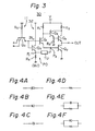
- FIG. 3 is a circuit diagram of a TTL circuit according to a first embodiment of the present invention.
- TTL circuit 30 is comprised of logic part 11 and main inverting amplifier 32.
- Reference symbol Q o represents a multi-emitter transistor in logic part 11.
- Logic part 11 is provided at its input side with, for example, on OR or AND logic circuit (not shown) and forms, with main inverting amplifier 32, a NOR gate or NAND gate.
- Reference symbol Q 1 represents the phase-inverting transistor, Q 2 the first output transistor, and Q 4 the second output transistor.
- Transistor Q 3 is a Darlington connection transistor together with second output transistor Q 4 .
- phase-inverting transistor Q 1 acts as a logic part of the TTL circuit
- transistors Q 1 , Q 2 , Q 3 and Q 4 act as a main inverting amplifier thereof.
- pull-down circuit PD according to the first embodiment is comprised of, first, two-terminal unit (impedance means) TU and, second, a control circuit made of control transistor Q s and resistor R 4 connected in series therewith.
- Figures 4A, 4B, 4C, 4D, 4E, and 4F illustrate six examples of two-terminal unit TU of Figure 3.
- Figure 4A illustrates a SBD, Figure 4B a diode, and Figure 4C a capacitor. These are all conventional.
- Two-terminal impedance units TU in accordance with the present invention are shown in Figures 4D, E and F with Figure 4D showing a resistor, Figure 4E a parallel circuit of a resistor and a capacitor, and Figure 4F a parallel circuit of a resistor and a diode.
- voltage level V IN of input signal IN is often higher when it indicates logic "L” than base-emitter voltage V BE5 of transistor Q 5 .
- transistor Q 5 will finally turn on and, therefore, the electric charges at the base of transistor Q 5 cannot be discharged via two-terminal unitTU and resistor R 4 .
- the desired pull-down operation may not be achieved.
- transistor Q 5 is momentarily turned off during the fall of voltage level V IN . Therefore, the electric charges at the base of first output transistor Q 2 are momentarily discharged when transistor Q 5 is off. This is because the voltage level at the emitter of transistor Q 5 cannot quickly follow the fall of voltage level V IN .
- V TU denotes a voltage drop across two-terminal unit TU created by the current
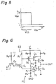
- Figure 5 is a graph representing the input-output characteristics obtained by the circuit shown in Fig. 3.
- the curve of Fig. 5 includes no slope-as shown in Fig. 2.
- the voltage level at junction points P 1 and P 2 which are each adjacent to a terminal of two-terminal unit TU, are the same as previously explained.
- the voltage level at junction point P 2 is higher than the level of ground GND by V BE2 , the base-emitter voltage of first output transistor Q 2 .
- Voltage level V IN of input signal IN is clamped to a level higher than the level at junction point P 2 by V BE1 , the base-emitter voltage of transistor Q 1 .
- the voltage level at junction point P 1 is lower than voltage level V IN by V BE5 , of the base-emitter voltage of transistor Q 5 .
- the base-emitter voltages of these transistors are usually the same value, i.e., V BE . Accordingly, the voltage levels at junction points P 1 and P 2 are both higher than the level of ground GND by V BE . In such a state, when voltage level V IN of input signal IN changes from "H" to "L", the voltage level at junction point P 1 changes to the ground level via resistor R 4 .
- a current can flow through the diode until the voltage at junction point P 2 reaches forward voltage V f of the diode.
- This current is not a long-term, continuous current, but a short-term current.
- said voltage level at junction point P 2 that is V f
- V INL denotes the "L" level of input signal IN.
- the short-term current is enough for discharging at least the stored electric charges at the base of first output transistor Q 2 .
- the diode has a static capacity (that is, a so-called p-n junction capacity)
- the stored electric charges at least, can be discharged with the charging current for said static capacity when the voltage level of input signal IN changes to the "L" level.
- the resistor of Fig. 4D is employed for two-terminal unit TU, it is difficult to obtain a function for discharging the stored electric charges, especially during said transient term. However, it is easy to discharge the stored electric charges, after which the voltage level difference between points P, and P 2 finally reaches a constant large value. From such a viewpoint, the parallel circuit of both the resistor and the capacitor, as shown in Fig. 4E, is preferable for two-terminal unit TU. In conclusion, it is most preferable that two-terminal unit TU be composed of the parallel circuit of both the resistor and the diode, as shown in Fig. 4F, because the diode is necessarily provided with the static capacity.
- Figure 6 is a circuit diagram of a TTL circuit according to a second embodiment of the present invention.
- members similar to those of Fig. 3 are represented by the same reference symbols and numerals as those of Fig. 3.
- pnp transistor Q 6 is newly employed instead of npn transistor Q 5 of Fig. 3.
- the operational principle of main inverting amplifier 62 in Fig. 6 is substantially the same as main inverting amplifier 32 in Fig. 3.
- a signal having the same phase as that of input signal IN is produced at junction point P 1 between two-terminal unit TU and resistor R 4 by way of pnp transistor Q 6 .
- phase-inverting transistor Q 1 when the level of input signal IN is "H", phase-inverting transistor Q 1 is turned on. Therefore, pnp transistor Q 6 is also turned on and the "L" level appears at junction point P 1 . This means that the signal at junction point P, has the same phase as that of input signal IN. Contrary to the above, when the level of input signal IN changes from “L” to “H”, phase-inverting transistor Q 1 starts turning on. At this time, a current would start flowing through two-terminal unit TU and resistor R 4 toward ground GND.
- phase-inverting transistor Q 1 cannot be turned on until first output transistor Q 2 is turned on. This means no undesired slope is created in the curve of output signal OUT when it changes from "H” to "L", as in the circuit of Fig. 3.
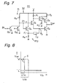
- FIG. 7 is a circuit diagram of another example of a TTL circuit to which the present invention is adapted.
- Figure 8 is a graph representing the input-output characteristics obtained by the circuit shown in Fig. 7.
- TTL circuit 70 comprised of logic part 71 and main inverting amplifier 32, is an example of a TTL circuit in which by the present invention is particularly advantageous.
- logic part 71 is comprised of pnp transistors Q 11 and Q 12 and resistor R o , rather than multi-emitter transistor Q o and resistor R o as in logic part 11 of Fig. 3.
- the prior art characteristic curves S 1 and S 2 of Fig. 2 can be improved, so as to obtain the stepwise characteristic curve shown in Fig. 5.
- This enables a considerably increased threshold voltage V th of input signal IN, used for determining the boundary of transition in "H" ⁇ "L” or "L" ⁇ ”H” of voltage level V OUT of output signal OUT.
- the threshold voltage V th shown in Fig. 5 is about 2 ⁇ V BE .
- TTL circuit 70 since logic part 71 is comprised of pnp transistors Q 11 and Q 12 , threshold voltage V th ' (see Fig. 8) of input signal IN' is lower than threshold voltage V th (see Figs. 5 and 8) of input signal IN. Therefore, in Fig. 8, if the undesired slope in the input-output characteristic curve is measured, as in curves S 1 and S 2 of Fig. 2, there would be almost no noise margin (refer to chain-dotted slope S in Fig. 8). However, according to the present invention, even though the threshold voltage is as low as voltage V th ', the noise margin can still be maintained, because the input-output characteristic curve changes stepwise.
- the pull-down circuit is operated selectively only when it is required, the input-output characteristics of the main inverting amplifier are improved and the noise margin can be increased. Further, since the slope of Fig. 2 no longer exists, it is not necessary to take the resistance value of resistor R 4 into account in determining the resistance value of resistor R 1 (because, as previously mentioned), the inclination degree of said slope is usually determined by the ratio between the resistance values of resistors R 1 and R 4 ). Accordingly, the resistance value of resistor R 1 is determined independently from that of resistor R 4 , which means increased flexibility in design work. Further, it is possible to increase the resistance value of resistor R 1 , because resistor R 1 is irrelevant to resistor R 4 .
- resistor R 4 If the resistance value of resistor R 1 is large, resistor R 4 is not needed to absorb, toward the ground, a large current therefrom. In other words, resistor R 4 can absorb a large amount of the stored electric charges at the base of transistor Q 2 , and, thereby, transistor Q 2 can quickly be turned from on to off. Thus, a sharp rising edge from "L" to "H” of output signal OUT can be realized.
Landscapes
- Engineering & Computer Science (AREA)
- Physics & Mathematics (AREA)
- Computer Hardware Design (AREA)
- Computing Systems (AREA)
- General Engineering & Computer Science (AREA)
- Mathematical Physics (AREA)
- Power Engineering (AREA)
- Logic Circuits (AREA)
Claims (1)
- Transistorschaltung mit einer Energieversorgungsleitung; einer Erdleitung; einem Eingangsanschluß; einem Ausgangsanschluß; einem Phasenumkehrtransistor (Q1), dessen Basis mit dem Eingangsanschluß verbunden ist; ersten (Q2) und zweiten (Q4) Ausgangstransistoren, die mit dem Ausgangsanschluß verbunden sind, wobei die ersten und zweiten Ausgangstransistoren so angeordnet sind, daß sie von entgegengesetztem Leitungszustand sind und, in Abhängigkeit von einem Ausgang des Phasenumkehrtransistors (Q1), EIN und AUS geschaltet werden; und einer Pull-down-Schaltung (PD) zum Entladen elektrischer Ladungen, die bei einer Basis des ersten Ausgangstransistors (Q2) enthalten sind, welche eine Steuerschaltung umfaßt, die einen Ausgangsknoten (P1) hat une ein Signal erzeugt, das dieselbe Phase wie das Eingangssignal bei dem Ausgangsknoten (P1) hat, und eine Zweipol-Impedanzeinrichtung (TU), die zwischen der Basis des ersten Ausgangstransistors (Q2) und dem Ausgangsknoten (P1) der Steuerschaltung (Q5) angeschlossen ist, dadurch gekennzeichnet, daß die Steuerschaltung einen Steuertransistor (Q5), der von demselben Leitfähigkeitstyp wie der des Phasenumkehrtransistors (Q1) ist und zwischen der Energieversorgungsleitung und dem Ausgangsknoten (P1) zur Erzeugung des Signals angeschlossen ist, das dieselbe Phase wie das Eingangssignal hat, und einen Widerstand (R4) umfaßt, der zwischen dem Ausgangsknoten (P1) und der Erdleitung angeschlossen ist, und daß die Zweipol-Impedanz-einrichtung (TU) einen Widerstand (Figur 4D), einen Kondensator und einen parallel geschalteten (Figur 4E) Widerstand, oder eine Diode und einen parallel geschalteten (Figur 4F) Widerstand umfaßt.
Applications Claiming Priority (2)
| Application Number | Priority Date | Filing Date | Title |
|---|---|---|---|
| JP128468/81 | 1981-08-17 | ||
| JP56128468A JPS5830233A (ja) | 1981-08-17 | 1981-08-17 | トランジスタ回路 |
Publications (3)
| Publication Number | Publication Date |
|---|---|
| EP0072694A2 EP0072694A2 (de) | 1983-02-23 |
| EP0072694A3 EP0072694A3 (en) | 1984-05-23 |
| EP0072694B1 true EP0072694B1 (de) | 1986-12-03 |
Family
ID=14985469
Family Applications (1)
| Application Number | Title | Priority Date | Filing Date |
|---|---|---|---|
| EP82304316A Expired EP0072694B1 (de) | 1981-08-17 | 1982-08-16 | Transistorschaltung |
Country Status (5)
| Country | Link |
|---|---|
| US (1) | US4535258A (de) |
| EP (1) | EP0072694B1 (de) |
| JP (1) | JPS5830233A (de) |
| DE (1) | DE3274607D1 (de) |
| IE (1) | IE53407B1 (de) |
Families Citing this family (6)
| Publication number | Priority date | Publication date | Assignee | Title |
|---|---|---|---|---|
| JPS59181724A (ja) * | 1983-03-31 | 1984-10-16 | Fujitsu Ltd | ゲ−トアレイlsi装置 |
| EP0128603A1 (de) * | 1983-05-13 | 1984-12-19 | Koninklijke Philips Electronics N.V. | TTL-Logikschaltung mit schaltbarer Stromrückkopplung |
| JPS63115420A (ja) * | 1986-10-31 | 1988-05-20 | Mitsubishi Electric Corp | バイポ−ラ論理回路 |
| NL8801103A (nl) * | 1988-04-28 | 1989-11-16 | Philips Nv | Transistorschakeling met stuurstroombegrenzing. |
| JP2820980B2 (ja) * | 1989-11-02 | 1998-11-05 | 富士通株式会社 | 論理回路 |
| JP5819212B2 (ja) * | 2012-02-13 | 2015-11-18 | アルプス電気株式会社 | 負荷接続状態検出回路 |
Citations (1)
| Publication number | Priority date | Publication date | Assignee | Title |
|---|---|---|---|---|
| EP0032043A1 (de) * | 1979-12-27 | 1981-07-15 | Fujitsu Limited | Logische Transistor-Transistor-Schaltung |
Family Cites Families (11)
| Publication number | Priority date | Publication date | Assignee | Title |
|---|---|---|---|---|
| FR1548667A (de) * | 1967-10-27 | 1968-12-06 | ||
| JPS4965770A (de) * | 1972-10-26 | 1974-06-26 | ||
| DE2545943A1 (de) * | 1975-10-14 | 1977-04-28 | Licentia Gmbh | Gatter |
| US4132906A (en) * | 1977-02-28 | 1979-01-02 | Motorola, Inc. | Circuit to improve rise time and/or reduce parasitic power supply spike current in bipolar transistor logic circuits |
| JPS54134549A (en) * | 1978-04-10 | 1979-10-19 | Fujitsu Ltd | Logical operation circuit |
| JPS54156463A (en) * | 1978-05-30 | 1979-12-10 | Nec Corp | Logic circuit |
| JPS55127731A (en) * | 1979-03-26 | 1980-10-02 | Hitachi Ltd | Logical operation circuit |
| US4449063A (en) * | 1979-08-29 | 1984-05-15 | Fujitsu Limited | Logic circuit with improved switching |
| JPS56122236A (en) * | 1980-02-29 | 1981-09-25 | Nec Corp | Logic gate circuit |
| US4413194A (en) * | 1981-07-10 | 1983-11-01 | Motorola, Inc. | TTL Output circuit having means for preventing output voltage excursions induced by negative current reflections |
| US4413195A (en) * | 1981-07-10 | 1983-11-01 | Motorola, Inc. | Transistor-transistor-logic circuits having improved breakdown protection circuitry |
-
1981
- 1981-08-17 JP JP56128468A patent/JPS5830233A/ja active Pending
-
1982
- 1982-08-16 EP EP82304316A patent/EP0072694B1/de not_active Expired
- 1982-08-16 DE DE8282304316T patent/DE3274607D1/de not_active Expired
- 1982-08-16 IE IE1979/82A patent/IE53407B1/en unknown
- 1982-08-17 US US06/408,846 patent/US4535258A/en not_active Expired - Fee Related
Patent Citations (1)
| Publication number | Priority date | Publication date | Assignee | Title |
|---|---|---|---|---|
| EP0032043A1 (de) * | 1979-12-27 | 1981-07-15 | Fujitsu Limited | Logische Transistor-Transistor-Schaltung |
Non-Patent Citations (1)
| Title |
|---|
| The New Peguin Dictionary of Electronics, 1979, pages 552-553 * |
Also Published As
| Publication number | Publication date |
|---|---|
| EP0072694A3 (en) | 1984-05-23 |
| IE821979L (en) | 1983-02-17 |
| EP0072694A2 (de) | 1983-02-23 |
| IE53407B1 (en) | 1988-11-09 |
| US4535258A (en) | 1985-08-13 |
| DE3274607D1 (en) | 1987-01-15 |
| JPS5830233A (ja) | 1983-02-22 |
Similar Documents
| Publication | Publication Date | Title |
|---|---|---|
| US4845386A (en) | Bi-MOS logic circuit having a totem pole type output buffer section | |
| US5041743A (en) | Emitter-follower circuit with reduced delay time | |
| KR910009086B1 (ko) | 출력회로 | |
| US4839537A (en) | BicMO logic circuit | |
| US4985645A (en) | BiCMOS logic circuit having a rapid output voltage falling-down property | |
| US4535258A (en) | Transistor-transistor logic circuit with improved switching times | |
| KR0142271B1 (ko) | 반도체 집적회로장치 | |
| US4883975A (en) | Schmitt trigger circuit | |
| US4709169A (en) | Logic level control for current switch emitter follower logic | |
| EP0239841B1 (de) | Spannungsausgabeschaltung | |
| EP0098155B1 (de) | Schmitt-Trigger-Schaltung | |
| EP0046498B1 (de) | Bootstrap-Treiberschaltung | |
| US5041747A (en) | Delay regulation circuit | |
| EP0302671A2 (de) | Logische Schaltung | |
| KR930009152B1 (ko) | Ecl논리회로 | |
| EP0054408B1 (de) | Logikschaltung | |
| US5126593A (en) | Method and circuitry for reducing output transients resulting from internal ground instabilities | |
| US4871929A (en) | ECL logic gate | |
| EP0432472A2 (de) | Integrierte CMOS-Ausgangsschaltung mit bipolaren Transistoren in der Ausgangsstufe | |
| US4897566A (en) | Bipolar transistor logic circuit | |
| JP2861300B2 (ja) | Mntl型半導体集積回路装置 | |
| KR890004653B1 (ko) | 논리회로 | |
| KR940006621B1 (ko) | Ecl 회로를 갖는 반도체 집적회로 | |
| EP0229726A1 (de) | Schaltung zum Angleichen der Signalverzögerungszeiten | |
| JPH0736519B2 (ja) | 電流スイツチ回路 |
Legal Events
| Date | Code | Title | Description |
|---|---|---|---|
| PUAI | Public reference made under article 153(3) epc to a published international application that has entered the european phase |
Free format text: ORIGINAL CODE: 0009012 |
|
| AK | Designated contracting states |
Designated state(s): DE FR GB |
|
| PUAL | Search report despatched |
Free format text: ORIGINAL CODE: 0009013 |
|
| AK | Designated contracting states |
Designated state(s): DE FR GB |
|
| 17P | Request for examination filed |
Effective date: 19840828 |
|
| GRAA | (expected) grant |
Free format text: ORIGINAL CODE: 0009210 |
|
| AK | Designated contracting states |
Kind code of ref document: B1 Designated state(s): DE FR GB |
|
| ET | Fr: translation filed | ||
| REF | Corresponds to: |
Ref document number: 3274607 Country of ref document: DE Date of ref document: 19870115 |
|
| PLBE | No opposition filed within time limit |
Free format text: ORIGINAL CODE: 0009261 |
|
| STAA | Information on the status of an ep patent application or granted ep patent |
Free format text: STATUS: NO OPPOSITION FILED WITHIN TIME LIMIT |
|
| 26N | No opposition filed | ||
| PGFP | Annual fee paid to national office [announced via postgrant information from national office to epo] |
Ref country code: FR Payment date: 19890830 Year of fee payment: 8 |
|
| PGFP | Annual fee paid to national office [announced via postgrant information from national office to epo] |
Ref country code: GB Payment date: 19890831 Year of fee payment: 8 |
|
| PGFP | Annual fee paid to national office [announced via postgrant information from national office to epo] |
Ref country code: DE Payment date: 19891027 Year of fee payment: 8 |
|
| PG25 | Lapsed in a contracting state [announced via postgrant information from national office to epo] |
Ref country code: GB Effective date: 19900816 |
|
| GBPC | Gb: european patent ceased through non-payment of renewal fee | ||
| PG25 | Lapsed in a contracting state [announced via postgrant information from national office to epo] |
Ref country code: FR Effective date: 19910430 |
|
| PG25 | Lapsed in a contracting state [announced via postgrant information from national office to epo] |
Ref country code: DE Effective date: 19910501 |
|
| REG | Reference to a national code |
Ref country code: FR Ref legal event code: ST |