EP0074065A2 - Schnellhärtungsverbundverfahren für Photoblitzanordnung - Google Patents
Schnellhärtungsverbundverfahren für Photoblitzanordnung Download PDFInfo
- Publication number
- EP0074065A2 EP0074065A2 EP82108010A EP82108010A EP0074065A2 EP 0074065 A2 EP0074065 A2 EP 0074065A2 EP 82108010 A EP82108010 A EP 82108010A EP 82108010 A EP82108010 A EP 82108010A EP 0074065 A2 EP0074065 A2 EP 0074065A2
- Authority
- EP
- European Patent Office
- Prior art keywords
- printed circuit
- circuit board
- metallic
- cure
- quick
- Prior art date
- Legal status (The legal status is an assumption and is not a legal conclusion. Google has not performed a legal analysis and makes no representation as to the accuracy of the status listed.)
- Withdrawn
Links
Images

Classifications
-
- H—ELECTRICITY
- H05—ELECTRIC TECHNIQUES NOT OTHERWISE PROVIDED FOR
- H05K—PRINTED CIRCUITS; CASINGS OR CONSTRUCTIONAL DETAILS OF ELECTRIC APPARATUS; MANUFACTURE OF ASSEMBLAGES OF ELECTRICAL COMPONENTS
- H05K3/00—Apparatus or processes for manufacturing printed circuits
- H05K3/10—Apparatus or processes for manufacturing printed circuits in which conductive material is applied to the insulating support in such a manner as to form the desired conductive pattern
- H05K3/20—Apparatus or processes for manufacturing printed circuits in which conductive material is applied to the insulating support in such a manner as to form the desired conductive pattern by affixing prefabricated conductor pattern
- H05K3/202—Apparatus or processes for manufacturing printed circuits in which conductive material is applied to the insulating support in such a manner as to form the desired conductive pattern by affixing prefabricated conductor pattern using self-supporting metal foil pattern
-
- G—PHYSICS
- G03—PHOTOGRAPHY; CINEMATOGRAPHY; ANALOGOUS TECHNIQUES USING WAVES OTHER THAN OPTICAL WAVES; ELECTROGRAPHY; HOLOGRAPHY
- G03B—APPARATUS OR ARRANGEMENTS FOR TAKING PHOTOGRAPHS OR FOR PROJECTING OR VIEWING THEM; APPARATUS OR ARRANGEMENTS EMPLOYING ANALOGOUS TECHNIQUES USING WAVES OTHER THAN OPTICAL WAVES; ACCESSORIES THEREFOR
- G03B15/00—Special procedures for taking photographs; Apparatus therefor
- G03B15/02—Illuminating scene
- G03B15/03—Combinations of cameras with lighting apparatus; Flash units
- G03B15/04—Combinations of cameras with non-electronic flash apparatus; Non-electronic flash units
- G03B15/0442—Constructional details of the flash apparatus; Arrangement of lamps, reflectors, or the like
-
- H—ELECTRICITY
- H05—ELECTRIC TECHNIQUES NOT OTHERWISE PROVIDED FOR
- H05K—PRINTED CIRCUITS; CASINGS OR CONSTRUCTIONAL DETAILS OF ELECTRIC APPARATUS; MANUFACTURE OF ASSEMBLAGES OF ELECTRICAL COMPONENTS
- H05K1/00—Printed circuits
- H05K1/02—Details
- H05K1/0213—Electrical arrangements not otherwise provided for
- H05K1/0263—High current adaptations, e.g. printed high current conductors or using auxiliary non-printed means; Fine and coarse circuit patterns on one circuit board
-
- H—ELECTRICITY
- H05—ELECTRIC TECHNIQUES NOT OTHERWISE PROVIDED FOR
- H05K—PRINTED CIRCUITS; CASINGS OR CONSTRUCTIONAL DETAILS OF ELECTRIC APPARATUS; MANUFACTURE OF ASSEMBLAGES OF ELECTRICAL COMPONENTS
- H05K1/00—Printed circuits
- H05K1/02—Details
- H05K1/09—Use of materials for the conductive, e.g. metallic pattern
-
- H—ELECTRICITY
- H05—ELECTRIC TECHNIQUES NOT OTHERWISE PROVIDED FOR
- H05K—PRINTED CIRCUITS; CASINGS OR CONSTRUCTIONAL DETAILS OF ELECTRIC APPARATUS; MANUFACTURE OF ASSEMBLAGES OF ELECTRICAL COMPONENTS
- H05K2203/00—Indexing scheme relating to apparatus or processes for manufacturing printed circuits covered by H05K3/00
- H05K2203/06—Lamination
- H05K2203/068—Features of the lamination press or of the lamination process, e.g. using special separator sheets
-
- H—ELECTRICITY
- H05—ELECTRIC TECHNIQUES NOT OTHERWISE PROVIDED FOR
- H05K—PRINTED CIRCUITS; CASINGS OR CONSTRUCTIONAL DETAILS OF ELECTRIC APPARATUS; MANUFACTURE OF ASSEMBLAGES OF ELECTRICAL COMPONENTS
- H05K3/00—Apparatus or processes for manufacturing printed circuits
- H05K3/38—Improvement of the adhesion between the insulating substrate and the metal
- H05K3/386—Improvement of the adhesion between the insulating substrate and the metal by the use of an organic polymeric bonding layer, e.g. adhesive
-
- Y—GENERAL TAGGING OF NEW TECHNOLOGICAL DEVELOPMENTS; GENERAL TAGGING OF CROSS-SECTIONAL TECHNOLOGIES SPANNING OVER SEVERAL SECTIONS OF THE IPC; TECHNICAL SUBJECTS COVERED BY FORMER USPC CROSS-REFERENCE ART COLLECTIONS [XRACs] AND DIGESTS
- Y10—TECHNICAL SUBJECTS COVERED BY FORMER USPC
- Y10T—TECHNICAL SUBJECTS COVERED BY FORMER US CLASSIFICATION
- Y10T29/00—Metal working
- Y10T29/49—Method of mechanical manufacture
- Y10T29/49002—Electrical device making
- Y10T29/49117—Conductor or circuit manufacturing
- Y10T29/49124—On flat or curved insulated base, e.g., printed circuit, etc.
- Y10T29/49128—Assembling formed circuit to base
-
- Y—GENERAL TAGGING OF NEW TECHNOLOGICAL DEVELOPMENTS; GENERAL TAGGING OF CROSS-SECTIONAL TECHNOLOGIES SPANNING OVER SEVERAL SECTIONS OF THE IPC; TECHNICAL SUBJECTS COVERED BY FORMER USPC CROSS-REFERENCE ART COLLECTIONS [XRACs] AND DIGESTS
- Y10—TECHNICAL SUBJECTS COVERED BY FORMER USPC
- Y10T—TECHNICAL SUBJECTS COVERED BY FORMER US CLASSIFICATION
- Y10T29/00—Metal working
- Y10T29/49—Method of mechanical manufacture
- Y10T29/49002—Electrical device making
- Y10T29/49117—Conductor or circuit manufacturing
- Y10T29/49124—On flat or curved insulated base, e.g., printed circuit, etc.
- Y10T29/49155—Manufacturing circuit on or in base
Definitions
- This invention relates to multi-lamp photoflash arrays and more particularly to a quick-cure laminating process for affixing a metallic circuit to a circuit board.
- a circuit board of a material such as a glass-fined epoxy serves as a suostrate and the metallic printeo circuit is affixed thereto.
- an adhesive material is applied to one surface of the printed circuit and pressure and heat are applied to the circuit and circuit board in an amount sufficient to cure the adhesive and effect attachment of the printed circuit to the circuit board.
- circuit board material specifications which permit a board thickness variation in the range of about plus or minus ten percent. Because of such relatively great variation in board thickness, it has been founa that virtually every circuit board has one or more low spots whereat contact with the adhesive covering the printed metallic circuit is not obtained. This lack of intimate contact between the adhesive-covered printed circuit and the circuit board has been found to greatly inhibit the rate of cure of the adhesive and, of course, causes a great extension of the time required for attachment between the printed circuit and the circuit board.
- the attachment of an adhesive-covered printed circuit to a circuit board utilizing a compression force tends to cause an undesired excess adhesive discharge.
- a kraft paper as a blotter to aDsorb this excess adhesive discharge.
- blotter material is an added cost, especially when replacement is necessary for each curing cycle, and obviously deleterious to an economical manufacturing operation.
- An object of the present invention is to provide an improved multi-lamp photoflash array. Another object of the invention is to reduce the time required to fabricate a multi-lamp photoflash array. Still another object of the invention is to enhance the manufacture of multi-lamp photoflash arrays. A further object of the invention is to reduce the time required to laminate a metallic printed circuit and a circuit board utilized in a photoflasn array.
- a quick-cure laminating process wherein an adhesive is applied to a metallic printed circuit, the printea circuit and a circuit boaro are positioned intermediate a pair of surfaces with the surface adjacent the printed circuit being an elastomeric material, compressed and heated for a time and at a temperature sufficient to cure the adhesive and affix the printed circuit to the board.
- an adhesive is applied to a metallic printed circuit which, along with a circuit board of elastomeric material, is positioned intermediate a pair of movable surfaces.
- the movable surfaces compress the printed circuit and circuit board at a pressure and temperature and for a time sufficient to cure the adhesive and affix the printed circuit to the circuit board.
- FIG. 1 illustrates a multi-lamp photoflash array.
- a circuit board 5 has a metallic printed circuit 7 affixed thereto and is positioned immediately adjacent a reflector unit 9.
- the reflector unit 9 includes a plurality of aligned cavities 11, each having a reflective surface 13 and a pair of conductor receiving apertures 15.
- a photoflash lamp 17 having a pair of electrical conductors 19 is disposed within each one of the cavities 11 with the electrical conductors 19 extending therethrough and contacting the metallic printed circuit 7.
- a light transmittable plastic housing member 21 encloses the reflector unit 9 and photoflash lamps 17, and is affixed to the circuit board 5. Thus, the printed circuit 7, the reflector unit 9 and the flashlamps 17 are contained intermediate the circuit board 5 and the housing member 21.
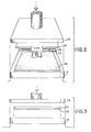
- a quick-cure laminating process includes therein a metallic printed circuit 23 such as may be obtained in a die-stamp operation utilizing an aluminum foil. Obviously, other materials and other techniques for deriving the printed circuit from the material are equally appropriate. Also, a curable adhesive 25 is applied to one surface of the printed circuit 23.
- the printed circuit board 27 may be of a moldable resin material, a resin-filled glass epoxy or numerous other materials well-known in the printed circuit board field. Moreover, the printed circuit 23 having the curable adhesive 25 thereon and the printed circuit board 27 are all positioned intermediate a pair of surfaces 29 and 31 movable with respect to one another. Moreover, the surfaces 29 and 31 are connected to a heating source (not shown) and to a source of compressive force (not shown).
- a deformable material layer 33 Positioned on one of the pair of surfaces 29 and 31 and adjacent the printed circuit 23 is a deformable material layer 33.
- This aeformable material layer 33 is of a material such as silicon rubber and, more specifically, of a material such as a fiberglass fabric high temperature elastomeric composite material known as Grade 55392R045, available from the Keene Corporation, Chase-Foster Division, Bear, Delaware 15701. Moreover, the above-mentioned elastomeric material is recommended for temperatures up to about 500° F for a limited period of time.
- the laminating process includes the application of a curable adhesive 25 to one surface of the metallic printed circuit 23.
- the adhesive-covered printed circuit 23 is positioned with the adhesive 25 adjacent a circuit board 27. Thereafter, the printed circuit 23 and circuit board 27 are located intermediate the pair of surfaces 29 and 31 which are movable with respect to one another.
- the layer of elastomeric material 33 positioned on the surface 31 of the pair of surfaces 29 and 31 is adjacent the printed circuit 23.
- the surfaces 29 and 31 are moved toward one another in an amount sufficient to exert a compressive force in the rance of aoout 100 to 500 pounds per square inch on the printed circuit 23 and circuit board 27.
- the printed circuit 23 having the adhesive 25 thereon and the circuit board 27 are heated in an amount and for a time sufficient to cause the printed circuit 23 to become affixed to the circuit board 27.
- the printed circuit 23 and circuit board 27 are heated to a temperature in the range of about 360 to 550° F. Moreover, the heating of the printed circuit 23 and circuit board 27 is effected for a period not greater than about 30 seconds and preferably for a period in the range of about 4 to 20 seconds. Thus, the printed circuit 23 and circuit board 27 are subjected to a compressive force in the range of about 100 to 500 pounds per square inch, a temperature in the range of about 360 to 550° F, and for a period not greater than about 30 seconds.
- FIG. 3 illustrates a quick-cure laminating process for multi-lamp photoflash arrays wherein the above-mentioned elastomeric material layer 33 of FIG. 2 is not required.
- an adhesive is applied to a surface of a printed circuit 35, and the printed circuit 35 is positioned adjacent a circuit board 37 of a deformable material:
- a preferred deformable material circuit board 37 is known as "Duroid,” manufactured by the Rogers Corporation of Rogers, Connecticut 06263.
- the printed circuit 35 and circuit board 37 of deformable material are located intermediate a pair of surfaces 39 and 41 which are movable with respect to one another.
- the surfaces 39 and 41 are activated to exert a compressive force on the printed circuit 35 and circuit board 37 in the range of about 100 to 500 pounds per square inch.
- heat is applied to the printed circuit 35 and circuit board 37 in an amount and for a time sufficient to cure the adhesive and effect attachment therebetween.
- the simultaneous application to the printed circuit 35 and circuit board 37 of compressive force in tne range of about 100 to 500 pounds per square inch, at a temperature in the range of about 360 to 500° F and for a period not greater than about 30 seconds is sufficient to effect the desired attachment.
- the circuit board 37 of deformable material serves to contain the adhesive intermediate the printed circuit 35 and circuit board 37 thereby eliminating the need for a blotter or other forms of adhesive absorbed.
- An enhanced quick-cure laminating process for multi-lamp photoflash arrays has been provided wherein a metallic printed circuit is attachable to a circuit board in a period of less than about 30 seconds.
- the process not only provides a very great reduction in cycle time required to effect such a printed circuit-circuit board attachment, but also provides an obvious improvement in manufacture and manufacturing cost.
- the utilization of a deformable material in the manufacturing process virtually eliminates the need for blotter materials for absorbing excess adhesives which, in turn, further reduces materials and material costs.
Landscapes
- Engineering & Computer Science (AREA)
- Manufacturing & Machinery (AREA)
- Microelectronics & Electronic Packaging (AREA)
- Physics & Mathematics (AREA)
- General Physics & Mathematics (AREA)
- Lining Or Joining Of Plastics Or The Like (AREA)
- Manufacturing Of Printed Wiring (AREA)
- Laminated Bodies (AREA)
Applications Claiming Priority (2)
| Application Number | Priority Date | Filing Date | Title |
|---|---|---|---|
| US298864 | 1981-09-03 | ||
| US06/298,864 US4935090A (en) | 1981-09-03 | 1981-09-03 | Photoflash array quick-cure laminating process |
Publications (2)
| Publication Number | Publication Date |
|---|---|
| EP0074065A2 true EP0074065A2 (de) | 1983-03-16 |
| EP0074065A3 EP0074065A3 (de) | 1984-02-22 |
Family
ID=23152296
Family Applications (1)
| Application Number | Title | Priority Date | Filing Date |
|---|---|---|---|
| EP82108010A Withdrawn EP0074065A3 (de) | 1981-09-03 | 1982-08-31 | Schnellhärtungsverbundverfahren für Photoblitzanordnung |
Country Status (4)
| Country | Link |
|---|---|
| US (1) | US4935090A (de) |
| EP (1) | EP0074065A3 (de) |
| JP (1) | JPS5882595A (de) |
| CA (1) | CA1204919A (de) |
Cited By (1)
| Publication number | Priority date | Publication date | Assignee | Title |
|---|---|---|---|---|
| EP0802711A3 (de) * | 1996-04-19 | 1999-08-18 | Matsushita Electric Industrial Co., Ltd. | Schaltbrett und Herstellungsverfahren |
Families Citing this family (6)
| Publication number | Priority date | Publication date | Assignee | Title |
|---|---|---|---|---|
| US5470644A (en) * | 1994-04-21 | 1995-11-28 | Durant; David | Apparatus and method for fabrication of printed circuit boards |
| US5607538A (en) * | 1995-09-07 | 1997-03-04 | Ford Motor Company | Method of manufacturing a circuit assembly |
| US6059917A (en) * | 1995-12-08 | 2000-05-09 | Texas Instruments Incorporated | Control of parallelism during semiconductor die attach |
| US5882954A (en) * | 1997-10-06 | 1999-03-16 | Ford Motor Company | Method for adhering a metallization to a substrate |
| US5903440A (en) * | 1998-01-30 | 1999-05-11 | Delco Electronics Corporaiton | Method of forming assemblies of circuit boards in different planes |
| DE10118866A1 (de) * | 2001-04-18 | 2002-10-24 | Swoboda Gmbh Geb | Verfahren zur Herstellung einer Radarantenne |
Family Cites Families (16)
| Publication number | Priority date | Publication date | Assignee | Title |
|---|---|---|---|---|
| US2957227A (en) * | 1955-07-15 | 1960-10-25 | Benjamin B Scott | Method of making electrical resistance cards |
| US2969300A (en) * | 1956-03-29 | 1961-01-24 | Bell Telephone Labor Inc | Process for making printed circuits |
| DE1082046B (de) * | 1958-06-04 | 1960-05-19 | Henkel & Cie Gmbh | Verfahren zur Verbesserung der Wasservertraeglichkeit von Aminotriazin-Aldehyd-Kondensaten |
| US3059320A (en) * | 1958-06-23 | 1962-10-23 | Ibm | Method of making electrical circuit |
| FR1260273A (fr) * | 1960-05-11 | 1961-05-05 | Ici Ltd | Coussins pour presses applicables à la fabrication d'objets stratifiés par pressage à chaud ou à froid |
| CH475846A (de) * | 1965-07-05 | 1969-07-31 | Dynamit Nobel Ag | Polyamidplatte oder -rohr, als Träger für Kupferschichten bestimmt |
| US3547724A (en) * | 1967-02-07 | 1970-12-15 | Rogers Corp | Method of and apparatus for producing printed circuits |
| US3962520A (en) * | 1973-06-20 | 1976-06-08 | Sumitomo Bakelite Company, Limited | Adhesive composition for flexible printed circuit and method for using the same |
| US3940534A (en) * | 1973-11-07 | 1976-02-24 | G. T. Schjeldahl Company | Electrical laminate |
| US3969177A (en) * | 1974-06-24 | 1976-07-13 | International Business Machines Corporation | Laminating method |
| US4159921A (en) * | 1975-08-06 | 1979-07-03 | Sharp Kabushiki Kaisha | Method of connecting an element having multiple terminals and a multi-lead flexible connector |
| US4016021A (en) * | 1976-03-29 | 1977-04-05 | Fleur Lee | Heat sealing unit and method of making same |
| US4078962A (en) * | 1976-11-05 | 1978-03-14 | Seal Incorporated | Vacuum press |
| US4302794A (en) * | 1979-09-04 | 1981-11-24 | Gte Products Corporation | Linear multilamp photoflash unit |
| US4325771A (en) * | 1980-03-19 | 1982-04-20 | Gte Products Corporation | Method of making a die-stamped circuit board assembly for photoflash devices |
| US4320572A (en) * | 1980-03-19 | 1982-03-23 | Gte Products Corporation | Die-stamped circuit board assembly having relief means-method of making |
-
1981
- 1981-09-03 US US06/298,864 patent/US4935090A/en not_active Expired - Fee Related
-
1982
- 1982-08-31 EP EP82108010A patent/EP0074065A3/de not_active Withdrawn
- 1982-09-02 CA CA000410675A patent/CA1204919A/en not_active Expired
- 1982-09-03 JP JP57152890A patent/JPS5882595A/ja active Pending
Cited By (1)
| Publication number | Priority date | Publication date | Assignee | Title |
|---|---|---|---|---|
| EP0802711A3 (de) * | 1996-04-19 | 1999-08-18 | Matsushita Electric Industrial Co., Ltd. | Schaltbrett und Herstellungsverfahren |
Also Published As
| Publication number | Publication date |
|---|---|
| US4935090A (en) | 1990-06-19 |
| CA1204919A (en) | 1986-05-27 |
| EP0074065A3 (de) | 1984-02-22 |
| JPS5882595A (ja) | 1983-05-18 |
Similar Documents
| Publication | Publication Date | Title |
|---|---|---|
| KR100418148B1 (ko) | 2개이상의케이싱부분으로형성되는제어장치 | |
| US5569886A (en) | Flexible printed circuit board | |
| GR3015668T3 (en) | Rigid-flexible printed circuit and process of forming such a circuit. | |
| CA2428723C (en) | Lamp on sheet and manufacturing method thereof | |
| AU603450B2 (en) | Mounting for printed circuit forming a heat sink with controlled expansion | |
| US4236046A (en) | High capacitance bus bar | |
| US6478909B1 (en) | Method for surface mounting electrical components to a substrate | |
| JP2001057406A (ja) | 放熱基板及びその製造方法 | |
| JPS62229861A (ja) | 集積回路パッケージの製作方法 | |
| JPH05206343A (ja) | ヒートシンク、電子組立体およびその組立て方法 | |
| EP0135688A3 (de) | Verfahren zur Herstellung einer elektrolumineszenten Lampe | |
| US4935090A (en) | Photoflash array quick-cure laminating process | |
| KR910009127A (ko) | 인쇄 회로판, 그의 제조방법 및 인쇄 회로판에 전자 부품을 부착시키는 방법 | |
| CN216357503U (zh) | 一种功率半导体器件安装结构 | |
| WO2020178279A1 (en) | Flexible printed circuit board assembly | |
| KR950703270A (ko) | 다층 프린트된 와이어 보오드를 제조하는 방법 | |
| JP2004327760A (ja) | Ledランプの製造法 | |
| GB1210175A (en) | Printed wiring panels | |
| CN214688314U (zh) | 一种高散热低介质常数覆铜板 | |
| TW342363B (en) | Process and device for producing laminates | |
| CA1208318A (en) | Mounting dielectric resonators | |
| JP2613846B2 (ja) | 電極シート片付きチップ型電子部品 | |
| US20210059070A1 (en) | Heat dissipation module and assembly method thereof | |
| JPH0128545Y2 (de) | ||
| JP3677415B2 (ja) | 大電流用回路基板およびその製造方法 |
Legal Events
| Date | Code | Title | Description |
|---|---|---|---|
| PUAI | Public reference made under article 153(3) epc to a published international application that has entered the european phase |
Free format text: ORIGINAL CODE: 0009012 |
|
| 17P | Request for examination filed |
Effective date: 19820831 |
|
| AK | Designated contracting states |
Designated state(s): BE DE FR GB NL |
|
| PUAL | Search report despatched |
Free format text: ORIGINAL CODE: 0009013 |
|
| AK | Designated contracting states |
Designated state(s): BE DE FR GB NL |
|
| STAA | Information on the status of an ep patent application or granted ep patent |
Free format text: STATUS: THE APPLICATION HAS BEEN WITHDRAWN |
|
| 18W | Application withdrawn |
Withdrawal date: 19860904 |
|
| RIN1 | Information on inventor provided before grant (corrected) |
Inventor name: BROWER, BOYD G. |