EP0622980B1 - Verfahren zum Montieren eines elektronischen Bauelements auf einer flexiblen Leiterplatte - Google Patents
Verfahren zum Montieren eines elektronischen Bauelements auf einer flexiblen Leiterplatte Download PDFInfo
- Publication number
- EP0622980B1 EP0622980B1 EP94106414A EP94106414A EP0622980B1 EP 0622980 B1 EP0622980 B1 EP 0622980B1 EP 94106414 A EP94106414 A EP 94106414A EP 94106414 A EP94106414 A EP 94106414A EP 0622980 B1 EP0622980 B1 EP 0622980B1
- Authority
- EP
- European Patent Office
- Prior art keywords
- printed circuit
- face
- resist layer
- insulating resist
- insulation film
- Prior art date
- Legal status (The legal status is an assumption and is not a legal conclusion. Google has not performed a legal analysis and makes no representation as to the accuracy of the status listed.)
- Expired - Lifetime
Links
Images
Classifications
-
- H—ELECTRICITY
- H05—ELECTRIC TECHNIQUES NOT OTHERWISE PROVIDED FOR
- H05K—PRINTED CIRCUITS; CASINGS OR CONSTRUCTIONAL DETAILS OF ELECTRIC APPARATUS; MANUFACTURE OF ASSEMBLAGES OF ELECTRICAL COMPONENTS
- H05K3/00—Apparatus or processes for manufacturing printed circuits
- H05K3/30—Assembling printed circuits with electric components, e.g. with resistors
- H05K3/32—Assembling printed circuits with electric components, e.g. with resistors electrically connecting electric components or wires to printed circuits
- H05K3/321—Assembling printed circuits with electric components, e.g. with resistors electrically connecting electric components or wires to printed circuits by conductive adhesives
-
- H—ELECTRICITY
- H05—ELECTRIC TECHNIQUES NOT OTHERWISE PROVIDED FOR
- H05K—PRINTED CIRCUITS; CASINGS OR CONSTRUCTIONAL DETAILS OF ELECTRIC APPARATUS; MANUFACTURE OF ASSEMBLAGES OF ELECTRICAL COMPONENTS
- H05K1/00—Printed circuits
- H05K1/02—Details
- H05K1/11—Printed elements for providing electric connections to or between printed circuits
- H05K1/111—Pads for surface mounting, e.g. lay-out
- H05K1/112—Pads for surface mounting, e.g. lay-out directly combined with via connections
- H05K1/114—Pad being close to via, but not surrounding the via
-
- H—ELECTRICITY
- H05—ELECTRIC TECHNIQUES NOT OTHERWISE PROVIDED FOR
- H05K—PRINTED CIRCUITS; CASINGS OR CONSTRUCTIONAL DETAILS OF ELECTRIC APPARATUS; MANUFACTURE OF ASSEMBLAGES OF ELECTRICAL COMPONENTS
- H05K3/00—Apparatus or processes for manufacturing printed circuits
- H05K3/22—Secondary treatment of printed circuits
- H05K3/24—Reinforcing of the conductive pattern
- H05K3/245—Reinforcing conductive patterns made by printing techniques or by other techniques for applying conductive pastes, inks or powders; Reinforcing other conductive patterns by such techniques
-
- H—ELECTRICITY
- H05—ELECTRIC TECHNIQUES NOT OTHERWISE PROVIDED FOR
- H05K—PRINTED CIRCUITS; CASINGS OR CONSTRUCTIONAL DETAILS OF ELECTRIC APPARATUS; MANUFACTURE OF ASSEMBLAGES OF ELECTRICAL COMPONENTS
- H05K1/00—Printed circuits
- H05K1/02—Details
- H05K1/03—Use of materials for the substrate
- H05K1/0393—Flexible materials
-
- H—ELECTRICITY
- H05—ELECTRIC TECHNIQUES NOT OTHERWISE PROVIDED FOR
- H05K—PRINTED CIRCUITS; CASINGS OR CONSTRUCTIONAL DETAILS OF ELECTRIC APPARATUS; MANUFACTURE OF ASSEMBLAGES OF ELECTRICAL COMPONENTS
- H05K1/00—Printed circuits
- H05K1/02—Details
- H05K1/09—Use of materials for the conductive, e.g. metallic pattern
- H05K1/092—Dispersed materials, e.g. conductive pastes or inks
- H05K1/095—Dispersed materials, e.g. conductive pastes or inks for polymer thick films, i.e. having a permanent organic polymeric binder
-
- H—ELECTRICITY
- H05—ELECTRIC TECHNIQUES NOT OTHERWISE PROVIDED FOR
- H05K—PRINTED CIRCUITS; CASINGS OR CONSTRUCTIONAL DETAILS OF ELECTRIC APPARATUS; MANUFACTURE OF ASSEMBLAGES OF ELECTRICAL COMPONENTS
- H05K1/00—Printed circuits
- H05K1/18—Printed circuits structurally associated with non-printed electric components
- H05K1/181—Printed circuits structurally associated with non-printed electric components associated with surface mounted components
-
- H—ELECTRICITY
- H05—ELECTRIC TECHNIQUES NOT OTHERWISE PROVIDED FOR
- H05K—PRINTED CIRCUITS; CASINGS OR CONSTRUCTIONAL DETAILS OF ELECTRIC APPARATUS; MANUFACTURE OF ASSEMBLAGES OF ELECTRICAL COMPONENTS
- H05K2201/00—Indexing scheme relating to printed circuits covered by H05K1/00
- H05K2201/09—Shape and layout
- H05K2201/09209—Shape and layout details of conductors
- H05K2201/09372—Pads and lands
- H05K2201/09436—Pads or lands on permanent coating which covers the other conductors
-
- H—ELECTRICITY
- H05—ELECTRIC TECHNIQUES NOT OTHERWISE PROVIDED FOR
- H05K—PRINTED CIRCUITS; CASINGS OR CONSTRUCTIONAL DETAILS OF ELECTRIC APPARATUS; MANUFACTURE OF ASSEMBLAGES OF ELECTRICAL COMPONENTS
- H05K2201/00—Indexing scheme relating to printed circuits covered by H05K1/00
- H05K2201/10—Details of components or other objects attached to or integrated in a printed circuit board
- H05K2201/10007—Types of components
- H05K2201/10106—Light emitting diode [LED]
-
- H—ELECTRICITY
- H05—ELECTRIC TECHNIQUES NOT OTHERWISE PROVIDED FOR
- H05K—PRINTED CIRCUITS; CASINGS OR CONSTRUCTIONAL DETAILS OF ELECTRIC APPARATUS; MANUFACTURE OF ASSEMBLAGES OF ELECTRICAL COMPONENTS
- H05K2201/00—Indexing scheme relating to printed circuits covered by H05K1/00
- H05K2201/10—Details of components or other objects attached to or integrated in a printed circuit board
- H05K2201/10613—Details of electrical connections of non-printed components, e.g. special leads
- H05K2201/10621—Components characterised by their electrical contacts
- H05K2201/10651—Component having two leads, e.g. resistor, capacitor
-
- H—ELECTRICITY
- H05—ELECTRIC TECHNIQUES NOT OTHERWISE PROVIDED FOR
- H05K—PRINTED CIRCUITS; CASINGS OR CONSTRUCTIONAL DETAILS OF ELECTRIC APPARATUS; MANUFACTURE OF ASSEMBLAGES OF ELECTRICAL COMPONENTS
- H05K2201/00—Indexing scheme relating to printed circuits covered by H05K1/00
- H05K2201/10—Details of components or other objects attached to or integrated in a printed circuit board
- H05K2201/10613—Details of electrical connections of non-printed components, e.g. special leads
- H05K2201/10954—Other details of electrical connections
- H05K2201/10977—Encapsulated connections
-
- H—ELECTRICITY
- H05—ELECTRIC TECHNIQUES NOT OTHERWISE PROVIDED FOR
- H05K—PRINTED CIRCUITS; CASINGS OR CONSTRUCTIONAL DETAILS OF ELECTRIC APPARATUS; MANUFACTURE OF ASSEMBLAGES OF ELECTRICAL COMPONENTS
- H05K2203/00—Indexing scheme relating to apparatus or processes for manufacturing printed circuits covered by H05K3/00
- H05K2203/02—Details related to mechanical or acoustic processing, e.g. drilling, punching, cutting, using ultrasound
- H05K2203/0285—Using ultrasound, e.g. for cleaning, soldering or wet treatment
-
- H—ELECTRICITY
- H05—ELECTRIC TECHNIQUES NOT OTHERWISE PROVIDED FOR
- H05K—PRINTED CIRCUITS; CASINGS OR CONSTRUCTIONAL DETAILS OF ELECTRIC APPARATUS; MANUFACTURE OF ASSEMBLAGES OF ELECTRICAL COMPONENTS
- H05K2203/00—Indexing scheme relating to apparatus or processes for manufacturing printed circuits covered by H05K3/00
- H05K2203/06—Lamination
- H05K2203/065—Binding insulating layers without adhesive, e.g. by local heating or welding, before lamination of the whole PCB
-
- H—ELECTRICITY
- H05—ELECTRIC TECHNIQUES NOT OTHERWISE PROVIDED FOR
- H05K—PRINTED CIRCUITS; CASINGS OR CONSTRUCTIONAL DETAILS OF ELECTRIC APPARATUS; MANUFACTURE OF ASSEMBLAGES OF ELECTRICAL COMPONENTS
- H05K2203/00—Indexing scheme relating to apparatus or processes for manufacturing printed circuits covered by H05K3/00
- H05K2203/13—Moulding and encapsulation; Deposition techniques; Protective layers
- H05K2203/1305—Moulding and encapsulation
- H05K2203/1311—Foil encapsulation, e.g. of mounted components
-
- H—ELECTRICITY
- H05—ELECTRIC TECHNIQUES NOT OTHERWISE PROVIDED FOR
- H05K—PRINTED CIRCUITS; CASINGS OR CONSTRUCTIONAL DETAILS OF ELECTRIC APPARATUS; MANUFACTURE OF ASSEMBLAGES OF ELECTRICAL COMPONENTS
- H05K2203/00—Indexing scheme relating to apparatus or processes for manufacturing printed circuits covered by H05K3/00
- H05K2203/14—Related to the order of processing steps
- H05K2203/1453—Applying the circuit pattern before another process, e.g. before filling of vias with conductive paste, before making printed resistors
-
- H—ELECTRICITY
- H05—ELECTRIC TECHNIQUES NOT OTHERWISE PROVIDED FOR
- H05K—PRINTED CIRCUITS; CASINGS OR CONSTRUCTIONAL DETAILS OF ELECTRIC APPARATUS; MANUFACTURE OF ASSEMBLAGES OF ELECTRICAL COMPONENTS
- H05K3/00—Apparatus or processes for manufacturing printed circuits
- H05K3/40—Forming printed elements for providing electric connections to or between printed circuits
- H05K3/4038—Through-connections; Vertical interconnect access [VIA] connections
- H05K3/4053—Through-connections; Vertical interconnect access [VIA] connections by thick-film techniques
- H05K3/4069—Through-connections; Vertical interconnect access [VIA] connections by thick-film techniques for via connections in organic insulating substrates
-
- H—ELECTRICITY
- H05—ELECTRIC TECHNIQUES NOT OTHERWISE PROVIDED FOR
- H05K—PRINTED CIRCUITS; CASINGS OR CONSTRUCTIONAL DETAILS OF ELECTRIC APPARATUS; MANUFACTURE OF ASSEMBLAGES OF ELECTRICAL COMPONENTS
- H05K3/00—Apparatus or processes for manufacturing printed circuits
- H05K3/46—Manufacturing multilayer circuits
- H05K3/4644—Manufacturing multilayer circuits by building the multilayer layer by layer, i.e. build-up multilayer circuits
- H05K3/4664—Adding a circuit layer by thick film methods, e.g. printing techniques or by other techniques for making conductive patterns by using pastes, inks or powders
-
- Y—GENERAL TAGGING OF NEW TECHNOLOGICAL DEVELOPMENTS; GENERAL TAGGING OF CROSS-SECTIONAL TECHNOLOGIES SPANNING OVER SEVERAL SECTIONS OF THE IPC; TECHNICAL SUBJECTS COVERED BY FORMER USPC CROSS-REFERENCE ART COLLECTIONS [XRACs] AND DIGESTS
- Y10—TECHNICAL SUBJECTS COVERED BY FORMER USPC
- Y10T—TECHNICAL SUBJECTS COVERED BY FORMER US CLASSIFICATION
- Y10T29/00—Metal working
- Y10T29/49—Method of mechanical manufacture
- Y10T29/49002—Electrical device making
- Y10T29/49117—Conductor or circuit manufacturing
- Y10T29/49124—On flat or curved insulated base, e.g., printed circuit, etc.
- Y10T29/4913—Assembling to base an electrical component, e.g., capacitor, etc.
- Y10T29/49144—Assembling to base an electrical component, e.g., capacitor, etc. by metal fusion
Definitions
- This invention relates to a method for mounting an electronic component on a flexible printed circuit board which is to be used in an electronic apparatus or the like.
- a flexible printed circuit board (hereinafter referred to as an FPC) is able to be installed in the electronic apparatuses at a bent portion and an opening space with thin size and light weight. Therefore, the FPC is widely used in the electronic apparatuses.
- the electronic component can not be mounted by soldering directly on the conductive silver resin paste of the FPC. Therefore, in this FPC, the electronic component is mounted usually with the following steps:
- thermoplastic insulation film is deformed, and hence, another printed circuit can not be formed on the thermoplastic insulation film.
- the US-A-4 631 820 discloses mounting an electronic component on a printed circuit board, by means of an insulating connecting sheet laid over the connection and by heating the connection.
- the present invention provides a method for mounting electronic component on a flexible printed circuit board of the present invention comprises steps of:
- the terminal of the electronic component is connected with the second connecting part of the second printed circuit without any step of using the conductive adhesive and the conductive anisotropic adhesive. Therefore, in the present mounting method, neither the conventional expensive curing oven nor the special conductive suspension is required. Thereby, mounting work is made simple, and its cost is low. Furthermore, in the present mounting method, the terminal is disposed directly on the second connecting part, and both the one faces of the first and the second insulating resist layers, which are disposed sandwiched between the terminal and the second connecting part, are pressurized and heated via the second insulation film eliminating from deforming the first insulation film.
- the present mounting method plural printed circuits can be formed on the flexible printed circuit board, and the electrical connection between the terminal and the second connecting part is made strong and achieves high reliability. Furthermore, in the present mounting method, since there is no step of reinforcing a connecting portion having the terminal and the second connecting part with the insulating resin adhesive, the expensive curing oven is not required. Therefore, mounting-work is made simple, and its cost is low.
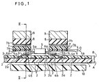
- FIG.1 is a partially cross-sectional view showing an arrangement of mounting members and an electronic component to be mounted on a flexible printed circuit board.
- FIG.2 is a vertical sectional view taken on line II-II in FIG.1.
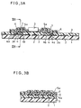
- FIG.3A is a partially cross-sectional view showing the completed state of the electronic component and the flexible printed circuit board.
- FIG.3B is a vertical sectional view taken on line IIIB-IIIB in FIG.3A.
- FIG.1 is a partially cross-sectional view showing an arrangement of mounting members and an electronic component to be mounted on a flexible printed circuit board.
- a first printed circuit 2 is formed on one face 1a of a first insulation film 1, which has a property of at least one of thermoplasticity and thermosetting property, by way of printing, such as screen printing or the like.
- the first printed circuit 2 and the one face 1a of the first insulation film 1 are covered with a first insulating resist layer 3, which has a property of at least one of thermoplasticity and a property of thermosetting and heating adhesion, by way of printing except a connecting part 2a of the first printed circuit 2.
- a second printed circuit 4 is formed on one face 3a of the first insulating resist layer 3 by way of printing so as to connect the connecting part 2a with a first connecting part 4a of the second printed circuit 4.
- an alternative method may be such that the whole of the first printed circuit 2 and the one face 1a of the first insulation film 1 are covered with the first insulating resist layer 3, and the second printed circuit 4 is formed on the one face 3a of the first insulating resist layer 3 by way of printing.
- a terminal 5a of an electronic component 5 is disposed on a second connecting part 4b of the second printed circuit 4.
- the flexible printed circuit board hereinafter referred to as the FPC
- four electronic components 5 are to be mounted on the FPC in parallel with each other in FIG.1 from the face side to the back side.
- the second insulation film 7 is disposed on the one face 3a of the first insulating resist layer 3 such that the second connecting part 4b and the terminal 5a are disposed between the one face 3a of the first insulating resist layer 3 and one face 6a of the second insulating resist layer 6.
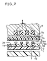
- FIG.2 is a vertical sectional view taken on line II-II in FIG.1.
- FIG.2 four elastic rubbers 8 are disposed with four recesses of an ultrasonic horn 9 provided at an end part of an ultrasonic welding apparatus, respectively.
- the ultrasonic horn 9 has high rigidity and substantially emits an ultrasonic wave.
- the ultrasonic horn 9 is disposed above the second face 7b of the second insulation film 7 so that the vertical center axes of four terminals 5a are disposed on the vertical center axes of four elastic rubbers 8, respectively.
- the ultrasonic horn 9 When the ultrasonic horn 9 comes in contact with the second face 7b of the second insulation film 7, the ultrasonic horn 9 presses the second face 7b of the second insulation film 7, and the ultrasonic wave heats the second face 7b of the second insulation film 7 so as to weld the one face 3a of the first insulating resist layer 3 and the one face 6a of the second insulating resist layer 6.
- four elastic rubbers 8 press the second face 7b of the second insulation film 7 so as to connect the terminal 5a with the second connecting part 4b tightly.
- the mounting work is done on a rigid supporting stand 10.
- FIG.3A is a partially cross-sectional view showing the completed state of the electronic component and the flexible printed circuit board.
- FIG.3B is a vertical sectional view taken on line IIIB-IIIB in FIG.3A.
- the terminal 5a is connected with the second connecting part 4b, and the first connecting part 4a is connected with the connecting part 2a.
- the first insulating resist layer 3 In the welding of the first insulating resist layer 3 to the second insulating resist layer 6, deforming of the first insulation film 1 is not raised. This is because that the heat produced by the ultrasonic welding is transmitted only from the second insulation film 7 to the second insulating resist layer 6 and the first insulating resist layer 3, and that the heat is not transmitted to the first insulation film 1, because the application of the ultrasonic wave and pressing by the elastic rubbers 8 is limited to a very short time of, for example, 0.2 second.
- the second connecting part 4b is not connected with the first printed circuit 2 directly. Namely, in case the whole of the first printed circuit 2 and the one face 1a of the first insulation film 1 are covered with a first insulating resist layer 3, even if the electronic component 5 is mounted on the second printed circuit 4, the second printed circuit 4 is not connected with the first printed circuit 2.
- an alternative method may be such that the first printed circuit 2, which is a metallic foil, is formed on the one face 1a of the first insulation film 1 by an insulating resin adhesive.
- the electronic component and each materials of the FPC and lengths of the example shown in FIG.1 are as follows:
- the LED 5 is mounted on the FPC according to the present mounting method as follows:
- the ultrasonic welding apparatus :
- the first and the second insulating resist layers 3 and 6 are changed into the below-mentioned materials from the materials of the first embodiment.
- the other materials of the FPC, the LED 5 and the mounting method is all the same as the first embodiment.
- the same components and parts as those of the first embodiment are designated by the same numerals and corresponding descriptions similarly apply. Therefore, the same explanation is omitted.
- the first and the second insulating resist layers 3 and 6 are of "an insulating resist of a denatured epoxide urethane resin" (Type EP-2940 manufactured by TOYOBO CO., LTD is made adjunction and bridge formation with a chemical equivalent isocyanate.
- the second insulating resist layer 6 is changed into the below-mentioned material from the materials of the first embodiment.
- the other materials of the FPC, the LED 5 and the mounting method is all the same as the first embodiment.
- the same components and parts as those of the first embodiment are designated by the same numerals and corresponding descriptions similarly apply. Therefore, the same explanation is omitted.
- the second insulating resist layer 6 is of "an insulating resist of a denatured epoxide urethane resin" Type EP-2940 manufactured by TOYOBO CO., LTD is made adjunction and bridge formation with a chemical equivalent isocyanate.
- the a slide switch, a rheostat, a transistor and an integrated circuit are used as the electronic component instead of the LED 5, respectively.
- the materials of the FPC and the mounting method is all the same as the first embodiment.
- the same components and parts as those of the first embodiment are designated by the same numerals and corresponding descriptions similarly apply. Therefore, the same explanation is omitted.
- connecting strengths between the above-mentioned electronic components and the second printed circuit 4 is enough as well as the first embodiment.
- an aluminum board (not shown), which has a thickness of 0.5 mm, is settled below the back face of the first insulation film 1 with a pressure sensitive adhesive double coated tape (which is used type 500 of NITTO DENKHO CO., LTD.) in view of handling of an operation lever or an operation axe.
Landscapes
- Engineering & Computer Science (AREA)
- Microelectronics & Electronic Packaging (AREA)
- Manufacturing & Machinery (AREA)
- Non-Metallic Protective Coatings For Printed Circuits (AREA)
- Electric Connection Of Electric Components To Printed Circuits (AREA)
- Combinations Of Printed Boards (AREA)
Claims (8)
- Verfahren zum Montieren eines elektronischen Bauelements (5) auf einer flexiblen Leiterplatte, mit den Schritten:Bilden einer ersten gedruckten Schaltung (2) durch Bedrucken einer Seite (la) eines ersten Isolierfilms (1), der zumindest thermoplastisch und wärmeaushärtend ist;Abdecken der ersten gedruckten Schaltung (2) und der einen Seite (1a) der ersten Isolierfilms (1) durch Aufdrucken einer ersten isolierenden Resistschicht (3), die wenigstens thermoplastisch oder wärmeaushärtend oder unter Wärme klebend ist;Bilden einer zweiten gedruckten Schaltung (4) durch Bedrucken einer Seite (3a) der ersten isolierenden Resistschicht (3);Anordnen eines Anschlusses (5a) eines elektronischen Bauelements (5) auf einem zweiten Verbindungsteil (4b) der zweiten gedruckten Schaltung (4);Abdecken einer ersten Seite (7a) eines zweiten Isolierfilms (7), der wenigstens thermoplastisch oder wärmeaushärtend ist, mittels Aufdrucken einer zweiten isolierenden Resistschicht (6), die wenigstens thermoplastisch oder wärmeaushärtend oder unter Wärme klebend ist, und Anordnen des zweiten Isolierfilms (7) auf einer Seite (3a) der ersten isolierenden Resistschicht (3) derart, daß der zweite Verbindungsteil (4b) und der Anschluß (5a) zwischen der einen Seite (3a) der ersten isolierenden Resistschicht (3) und einer Seite (6a) der zweiten isolierenden Resistschicht (6) zu liegen kommen;Drücken bzw. Pressen einer zweiten Seite (7b) des zweiten Isolierfilms (7) derart, daß der Anschluß (5a) mit dem zweiten Verbindungsteil (4b) verbunden wird, und Erwärmen der zweiten Seite (7b) des zweiten Isolierfilms (7) derart, daß die eine Seite (3a) der ersten isolierenden Resistschicht (3) und die eine Seite (6a) der zweiten isolierenden Resistschicht (6) verschweißt werden.
- Verfahren zum Montieren eines elektronischen Bauelements auf einer flexiblen Leiterplatte, mit den Schritten:Bilden einer ersten gedruckten Schaltung (2) durch Bedrucken einer Seite (1a) eines ersten Isolierfilms (1), der zumindest thermoplastisch oder wärmeaushärtend ist;Abdecken der ersten gedruckten Schaltung (2) und der einen Seite (1a) des ersten Isolierfilms (1) durch Aufdrucken einer ersten isolierenden Resistschicht (3), die zumindest thermoplastisch oder wärmeaushärtend und unter Wärme klebend ist, mit Ausnahme eines Verbindungsteils (2a) der ersten gedruckten Schaltung (2);Bilden einer zweiten gedruckten Schaltung (4) durch Bedrucken einer ersten Seite (3a) der ersten isolierenden Resistschicht (3) derart, daß der Verbindungsteil (2a) mit einem ersten Verbindungsteil (4a) der zweiten gedruckten Schaltung (4) verbunden wird;Anordnen eines Anschlusses (5a) eines elektronischen Bauelements (5) auf einem zweiten Verbindungsteil (4b) der zweiten gedruckten Schaltung (4);Abdecken einer ersten Seite (7a) eines zweiten Isolierfilms (7), der wenigstens thermoplastisch oder wärmeaushärtend ist durch Aufdrucken mit einer zweiten isolierenden Resistschicht (6), die zumindest thermoplastisch oder wärmeaushärtend und unter Wärme klebend ist, und Anordnen des zweiten Isolierfilms (7) auf der einen Seite (3a) der ersten isolierenden Resistschicht (3) derart, daß der zweite Verbindungsteil (4b) und der Anschluß (5a) zwischen der einen Seite (3a) der ersten isolierenden Resistschicht (3) und der einen Seite (6a) der zweiten isolierenden Resistschicht (6) zu liegen kommen;Drücken bzw. Pressen einer zweiten Seite (7b) des zweiten Isolierfilms (7) derart, daß der Anschluß (5a) mit dem zweiten Verbindungsteil (4b) verbunden wird, und Erwärmen der zweiten Seite (7b) des zweiten Isolierfilms (7) derart, daß die eine Seite (3a) der ersten isolierenden Resistschicht (3) und die eine Seite (6a) der zweiten isolierenden Resistschicht (6) verschweißt werden.
- Verfahren zum Montieren eines elektronischen Bauelements auf einer flexiblen Leiterplatte nach Anspruch 1 und 2, wobei die Wärme durch Ultraschallschweißen erhalten wird.
- Verfahren zum Montieren eines elektronischen Bauelements auf einer flexiblen Leiterplatte nach Anspruch 1 und 2, wobei das Pressen durch ein elastisches Gummiteil (8) erzielt wird, und wobei das Erwärmen mit einem Ultraschallhorn (9) erzielt wird, das an einem Endteil einer Ultraschallschweißvorrichtung vorgesehen ist und ausreichend starr ist.
- Verfahren zum Montieren eines elektronischen Bauelements auf einer flexiblen Leiterplatte nach Anspruch 1 und 2, wobei das Bilden der ersten gedruckten Schaltung (2), bei der es sich um eine Metallfolie handelt, auf der einen Seite (1a) des ersten Isolierfilms (1), der zumindest thermoplastisch oder wärmeaushärtend ist, durch einen isolierenden Harzklebstoff erfolgt.
- Verfahren zum Montieren eines elektronischen Bauelements auf einer flexiblen Leiterplatte nach Anspruch 1 und 2, wobei die ersten und zweiten isolierenden Resistschichten (3, 6) Vinylchloridharz sind.
- Verfahren zum Montieren eines elektronischen Bauelements auf einer flexiblen Leiterplatte nach Anspruch 1 und 2, wobei die ersten und zweiten isolierenden Resistschichten (3, 6) denaturiertes Epoxidurethanharz sind.
- Flexible Leiterplatte mit:einem ersten Isolierfilm (1),einer ersten gedruckten Schaltung (2), die einen Verbindungsteil (2a) aufweist, wobei die erste gedruckte Schaltung (2) auf einer Seite (1a) eines ersten Isolierfilms (1) gebildet ist,einer ersten isolierenden Resistschicht (3), die eine Einführungsöffnung aufweist, wobei die erste isolierende Resistschicht (3) auf einer Seite (1a) des ersten Isolierfilms (1) und der ersten gedruckten Schaltung (2) derart gebildet ist, daß die Einführungsöffnung auf dem Verbindungsteil (2a) zu liegen kommt,einer zweiten gedruckten Schaltung (4), die wenigstens einen ersten Verbindungsteil (4a) und einen zweiten Verbindungsteil (4b) aufweist, wobei die zweite gedruckte Schaltung (4) auf einer Seite (3a) der ersten isolierenden Resistschicht (3) derart gebildet ist, daß der erste Verbindungsteil (4a) in Kontakt mit dem Verbindungsteil (2a) steht,einem elektronischen Bauelement (5), das einen Anschluß (5a) aufweist, wobei das elektronische Bauelement (5) auf der zweiten gedruckten Schaltung (4) derart angeordnet ist, daß der Anschluß (5a) in Kontakt mit dem zweiten Verbindungsteil (4b) steht, undeinem zweiten Isolierfilm (7), der eine zweite isolierende Resistschicht (6) aufweist, wobei die zweite isolierende Resistschicht (6) auf einer Seite (7a) des zweiten Isolierfilms (7) gebildet ist, wobei der zweite Isolierfilm (7) und die zweite isolierende Resistschicht (6) auf wenigstens dem Anschluß (5a) angeordnet sind, und wobei die zweite isolierende Resistschicht (6) mechanisch mit einer Seite (3a) der ersten isolierenden Resistschicht (3) mit einer geschweißten Grenzfläche dazwischen verbunden ist.
Applications Claiming Priority (2)
| Application Number | Priority Date | Filing Date | Title |
|---|---|---|---|
| JP100911/93 | 1993-04-27 | ||
| JP5100911A JPH06310839A (ja) | 1993-04-27 | 1993-04-27 | フレキシブル印刷回路板への電子部品の実装方法 |
Publications (2)
| Publication Number | Publication Date |
|---|---|
| EP0622980A1 EP0622980A1 (de) | 1994-11-02 |
| EP0622980B1 true EP0622980B1 (de) | 1997-07-09 |
Family
ID=14286529
Family Applications (1)
| Application Number | Title | Priority Date | Filing Date |
|---|---|---|---|
| EP94106414A Expired - Lifetime EP0622980B1 (de) | 1993-04-27 | 1994-04-25 | Verfahren zum Montieren eines elektronischen Bauelements auf einer flexiblen Leiterplatte |
Country Status (4)
| Country | Link |
|---|---|
| US (2) | US5461775A (de) |
| EP (1) | EP0622980B1 (de) |
| JP (1) | JPH06310839A (de) |
| DE (1) | DE69404082T2 (de) |
Families Citing this family (25)
| Publication number | Priority date | Publication date | Assignee | Title |
|---|---|---|---|---|
| JPH08335761A (ja) * | 1995-06-06 | 1996-12-17 | Matsushita Electric Ind Co Ltd | 電子部品の配線基板への装着方法およびこれを用いた照光式スイッチユニット |
| US5622652A (en) * | 1995-06-07 | 1997-04-22 | Img Group Limited | Electrically-conductive liquid for directly printing an electrical circuit component onto a substrate, and a method for making such a liquid |
| WO1997014157A1 (en) * | 1995-10-07 | 1997-04-17 | Img Group Limited | An electrical circuit component formed of a conductive liquid printed directly onto a substrate |
| JPH1027952A (ja) * | 1996-07-09 | 1998-01-27 | Sharp Corp | プリント配線板及びその製造方法 |
| EP0824301A3 (de) * | 1996-08-09 | 1999-08-11 | Hitachi, Ltd. | Gedruckte Schaltungsplatte, Chipkarte, und Verfahren zu deren Herstellung |
| JPH1056099A (ja) | 1996-08-12 | 1998-02-24 | Shinko Electric Ind Co Ltd | 多層回路基板およびその製造方法 |
| US7714235B1 (en) * | 1997-05-06 | 2010-05-11 | Formfactor, Inc. | Lithographically defined microelectronic contact structures |
| US6024702A (en) * | 1997-09-03 | 2000-02-15 | Pmt Corporation | Implantable electrode manufactured with flexible printed circuit |
| JP3435062B2 (ja) * | 1997-10-03 | 2003-08-11 | 矢崎総業株式会社 | シールド電線の接続構造及び接続方法並びに接続に用いられる超音波ホーン及び接続に用いる接地電線 |
| JP4301661B2 (ja) * | 1999-11-12 | 2009-07-22 | 富士通マイクロエレクトロニクス株式会社 | ボールグリッドアレイ構造のデバイスに使用されるコンタクトフィルム及びデバイス実装構造体 |
| US6824857B2 (en) | 2001-04-02 | 2004-11-30 | Nashua Corporation | Circuit elements having an embedded conductive trace and methods of manufacture |
| EP1383364A3 (de) * | 2002-05-23 | 2006-01-04 | Nashua Corporation | Schaltungselemente mit tintenaufnehmender Beschichtung und einer Leiterbahn und Verfahren zu deren Herstellung |
| DE10354118A1 (de) * | 2003-11-19 | 2005-06-02 | Ruwel Ag | Verfahren zur Herstellung von Leiterplatten und Leiterplatte |
| US7317577B2 (en) * | 2004-05-14 | 2008-01-08 | Eastman Kodak Company | Methods for producing a black matrix on a lenticular lens |
| DE102006004320A1 (de) * | 2006-01-31 | 2007-08-09 | Häusermann GmbH | Leiterplatte mit funktionalen Elementen und selektiv gefüllten und thermisch leitfähigen Durchsteigelöchern sowie Herstellverfahren und Anwendung |
| KR20090078819A (ko) * | 2006-10-10 | 2009-07-20 | 티아이알 테크놀로지 엘피 | 인쇄 회로 기판, 인쇄 회로 기판의 준비 방법, 및 인쇄 회로 기판의 조립 방법 |
| US8748909B2 (en) * | 2006-11-03 | 2014-06-10 | Apple Inc. | Display system |
| KR101110865B1 (ko) * | 2007-11-27 | 2012-02-15 | 엘이디라이텍(주) | 램프유닛 |
| TWI370714B (en) * | 2008-01-09 | 2012-08-11 | Ind Tech Res Inst | Circuit structure and menufacturing method thereof |
| KR101518457B1 (ko) * | 2008-06-12 | 2015-05-12 | 서울반도체 주식회사 | 발광 다이오드 실장용 연성인쇄회로기판 |
| JP2010061923A (ja) * | 2008-09-02 | 2010-03-18 | Three M Innovative Properties Co | 電気接続方法及び電気接続された接続構造体 |
| FR2961057B1 (fr) * | 2010-06-03 | 2016-01-29 | Nief Plastic | Procede de montage de composants electroniques ou electriques sur un support de circuit conducteur d'electricite |
| JP6243764B2 (ja) | 2014-03-18 | 2017-12-06 | デクセリアルズ株式会社 | 可撓性実装モジュール体の製造方法 |
| US11219761B2 (en) | 2016-05-11 | 2022-01-11 | Inspire Medical Systems, Inc. | Attenuation arrangement for implantable medical device |
| JP7511180B2 (ja) | 2020-07-27 | 2024-07-05 | パナソニックIpマネジメント株式会社 | 実装方法およびそれにより形成される実装構造体 |
Family Cites Families (16)
| Publication number | Priority date | Publication date | Assignee | Title |
|---|---|---|---|---|
| US3699010A (en) * | 1971-03-22 | 1972-10-17 | North American Rockwell | Beam lead plating process |
| US4631820A (en) * | 1984-08-23 | 1986-12-30 | Canon Kabushiki Kaisha | Mounting assembly and mounting method for an electronic component |
| US4774634A (en) * | 1986-01-21 | 1988-09-27 | Key Tronic Corporation | Printed circuit board assembly |
| JPS62169434A (ja) * | 1986-01-22 | 1987-07-25 | Sharp Corp | Lsi搭載方式 |
| US4855796A (en) * | 1986-06-06 | 1989-08-08 | Hughes Aircraft Company | Beam lead mixer diode |
| DE3785720T2 (de) * | 1986-09-25 | 1993-08-12 | Toshiba Kawasaki Kk | Verfahren zum herstellen eines filmtraegers. |
| JPS63158711A (ja) * | 1986-12-22 | 1988-07-01 | 帝国通信工業株式会社 | フレキシブルプリント基板の端子構造 |
| US4835847A (en) * | 1988-04-20 | 1989-06-06 | International Business Machines Corp. | Method and apparatus for mounting a flexible film electronic device carrier on a substrate |
| US4900878A (en) * | 1988-10-03 | 1990-02-13 | Hughes Aircraft Company | Circuit terminations having improved electrical and structural integrity |
| US4944087A (en) * | 1988-10-05 | 1990-07-31 | Rogers Corporation | Method of making a curved plastic body with circuit pattern |
| JP2594644B2 (ja) * | 1989-05-01 | 1997-03-26 | 日本黒鉛工業株式会社 | ピン付きヒートシールコネクタの製造方法 |
| JP2866873B2 (ja) * | 1989-07-19 | 1999-03-08 | 大四郎 藤島 | 食品の処理方法 |
| JP2501702Y2 (ja) * | 1989-09-28 | 1996-06-19 | ブラザー工業株式会社 | 回路基板 |
| US5049978A (en) * | 1990-09-10 | 1991-09-17 | General Electric Company | Conductively enclosed hybrid integrated circuit assembly using a silicon substrate |
| US5291375A (en) * | 1991-09-30 | 1994-03-01 | Kabushiki Kaisha Toshiba | Printed circuit board and electric device configured to facilitate bonding |
| JP3042132B2 (ja) * | 1992-02-10 | 2000-05-15 | 松下電器産業株式会社 | 回路基板への電気部品実装方法 |
-
1993
- 1993-04-27 JP JP5100911A patent/JPH06310839A/ja active Pending
-
1994
- 1994-04-19 US US08/230,033 patent/US5461775A/en not_active Expired - Lifetime
- 1994-04-25 DE DE69404082T patent/DE69404082T2/de not_active Expired - Fee Related
- 1994-04-25 EP EP94106414A patent/EP0622980B1/de not_active Expired - Lifetime
-
1995
- 1995-04-18 US US08/423,907 patent/US5569886A/en not_active Expired - Fee Related
Also Published As
| Publication number | Publication date |
|---|---|
| JPH06310839A (ja) | 1994-11-04 |
| US5569886A (en) | 1996-10-29 |
| DE69404082T2 (de) | 1997-10-30 |
| EP0622980A1 (de) | 1994-11-02 |
| DE69404082D1 (de) | 1997-08-14 |
| US5461775A (en) | 1995-10-31 |
Similar Documents
| Publication | Publication Date | Title |
|---|---|---|
| EP0622980B1 (de) | Verfahren zum Montieren eines elektronischen Bauelements auf einer flexiblen Leiterplatte | |
| EP0272707B1 (de) | Anordnung von End-Verbindern an flexiblen gedruckten Schaltungen | |
| US5354392A (en) | Method for connecting a wiring arranged on a sheet with another wiring arranged on another sheet by ultrasonic waves | |
| KR100634239B1 (ko) | 보강판 부착 장치 및 부착 방법 | |
| JP2000002882A (ja) | 液晶表示装置及びその製造方法 | |
| GB2255219A (en) | Bonding components in a liquid-crystal display device. | |
| US5258866A (en) | Method of connecting liquid crystal display and circuit board with thermal expansion compensation | |
| US6723251B2 (en) | Method for planarizing circuit board and method for manufacturing semiconductor device | |
| US5848462A (en) | Method for mounting an electronic component on a wiring substrate and an illuminating switch unit using this mounting method | |
| EP0675673A2 (de) | Verstärkung für flexible Leiterplatte und verstärkte flexible Leiterplatte | |
| JPH07221422A (ja) | プリント配線基板およびその製造方法 | |
| CN114786335B (zh) | 柔性电路板及其绑定方法、显示装置 | |
| JPH11345300A (ja) | Icカードの製造方法 | |
| JP2613846B2 (ja) | 電極シート片付きチップ型電子部品 | |
| JPH07162120A (ja) | フレキシブルプリント配線板の回路接続方法及びフレキシブルプリント配線板 | |
| JP2007035546A (ja) | 圧着装置及び圧着方法 | |
| JP3349365B2 (ja) | 液晶表示装置及びその製造方法 | |
| JPH0774446A (ja) | プリント配線板の接続構造 | |
| JP2597051B2 (ja) | 多層プリント回路基板 | |
| JP2001125127A (ja) | 液晶装置及びその接続方法 | |
| EP0501414A1 (de) | Verfahren für die Verbindung der Elektroden einer Anzeigeeinrichtung | |
| JPS63299189A (ja) | フレキシブル配線板の接続構造 | |
| JPH0537417Y2 (de) | ||
| JPS63299242A (ja) | 半導体装置の接続方法 | |
| JP2001076576A (ja) | メンブレンスイッチ及びその製造方法 |
Legal Events
| Date | Code | Title | Description |
|---|---|---|---|
| PUAI | Public reference made under article 153(3) epc to a published international application that has entered the european phase |
Free format text: ORIGINAL CODE: 0009012 |
|
| 17P | Request for examination filed |
Effective date: 19940425 |
|
| AK | Designated contracting states |
Kind code of ref document: A1 Designated state(s): DE FR GB |
|
| 17Q | First examination report despatched |
Effective date: 19951204 |
|
| GRAG | Despatch of communication of intention to grant |
Free format text: ORIGINAL CODE: EPIDOS AGRA |
|
| GRAH | Despatch of communication of intention to grant a patent |
Free format text: ORIGINAL CODE: EPIDOS IGRA |
|
| GRAH | Despatch of communication of intention to grant a patent |
Free format text: ORIGINAL CODE: EPIDOS IGRA |
|
| GRAA | (expected) grant |
Free format text: ORIGINAL CODE: 0009210 |
|
| AK | Designated contracting states |
Kind code of ref document: B1 Designated state(s): DE FR GB |
|
| ET | Fr: translation filed | ||
| REF | Corresponds to: |
Ref document number: 69404082 Country of ref document: DE Date of ref document: 19970814 |
|
| PLBE | No opposition filed within time limit |
Free format text: ORIGINAL CODE: 0009261 |
|
| STAA | Information on the status of an ep patent application or granted ep patent |
Free format text: STATUS: NO OPPOSITION FILED WITHIN TIME LIMIT |
|
| 26N | No opposition filed | ||
| REG | Reference to a national code |
Ref country code: GB Ref legal event code: IF02 |
|
| PGFP | Annual fee paid to national office [announced via postgrant information from national office to epo] |
Ref country code: FR Payment date: 20060410 Year of fee payment: 13 |
|
| PGFP | Annual fee paid to national office [announced via postgrant information from national office to epo] |
Ref country code: GB Payment date: 20060419 Year of fee payment: 13 |
|
| PGFP | Annual fee paid to national office [announced via postgrant information from national office to epo] |
Ref country code: DE Payment date: 20070419 Year of fee payment: 14 |
|
| GBPC | Gb: european patent ceased through non-payment of renewal fee |
Effective date: 20070425 |
|
| PG25 | Lapsed in a contracting state [announced via postgrant information from national office to epo] |
Ref country code: GB Free format text: LAPSE BECAUSE OF NON-PAYMENT OF DUE FEES Effective date: 20070425 |
|
| PG25 | Lapsed in a contracting state [announced via postgrant information from national office to epo] |
Ref country code: FR Free format text: LAPSE BECAUSE OF NON-PAYMENT OF DUE FEES Effective date: 20070430 |
|
| PG25 | Lapsed in a contracting state [announced via postgrant information from national office to epo] |
Ref country code: DE Free format text: LAPSE BECAUSE OF NON-PAYMENT OF DUE FEES Effective date: 20081101 |