EP0074399B1 - Bei nullstrom schaltender durchflussumrichter - Google Patents
Bei nullstrom schaltender durchflussumrichter Download PDFInfo
- Publication number
- EP0074399B1 EP0074399B1 EP82901257A EP82901257A EP0074399B1 EP 0074399 B1 EP0074399 B1 EP 0074399B1 EP 82901257 A EP82901257 A EP 82901257A EP 82901257 A EP82901257 A EP 82901257A EP 0074399 B1 EP0074399 B1 EP 0074399B1
- Authority
- EP
- European Patent Office
- Prior art keywords
- capacitor
- current
- voltage
- load
- converter circuit
- Prior art date
- Legal status (The legal status is an assumption and is not a legal conclusion. Google has not performed a legal analysis and makes no representation as to the accuracy of the status listed.)
- Expired
Links
Images

Classifications
-
- H—ELECTRICITY
- H02—GENERATION; CONVERSION OR DISTRIBUTION OF ELECTRIC POWER
- H02M—APPARATUS FOR CONVERSION BETWEEN AC AND AC, BETWEEN AC AND DC, OR BETWEEN DC AND DC, AND FOR USE WITH MAINS OR SIMILAR POWER SUPPLY SYSTEMS; CONVERSION OF DC OR AC INPUT POWER INTO SURGE OUTPUT POWER; CONTROL OR REGULATION THEREOF
- H02M3/00—Conversion of DC power input into DC power output
- H02M3/22—Conversion of DC power input into DC power output with intermediate conversion into AC
- H02M3/24—Conversion of DC power input into DC power output with intermediate conversion into AC by static converters
- H02M3/28—Conversion of DC power input into DC power output with intermediate conversion into AC by static converters using discharge tubes with control electrode or semiconductor devices with control electrode to produce the intermediate AC
- H02M3/325—Conversion of DC power input into DC power output with intermediate conversion into AC by static converters using discharge tubes with control electrode or semiconductor devices with control electrode to produce the intermediate AC using devices of a triode or a transistor type requiring continuous application of a control signal
- H02M3/335—Conversion of DC power input into DC power output with intermediate conversion into AC by static converters using discharge tubes with control electrode or semiconductor devices with control electrode to produce the intermediate AC using devices of a triode or a transistor type requiring continuous application of a control signal using semiconductor devices only
- H02M3/33538—Conversion of DC power input into DC power output with intermediate conversion into AC by static converters using discharge tubes with control electrode or semiconductor devices with control electrode to produce the intermediate AC using devices of a triode or a transistor type requiring continuous application of a control signal using semiconductor devices only of the forward type
-
- Y—GENERAL TAGGING OF NEW TECHNOLOGICAL DEVELOPMENTS; GENERAL TAGGING OF CROSS-SECTIONAL TECHNOLOGIES SPANNING OVER SEVERAL SECTIONS OF THE IPC; TECHNICAL SUBJECTS COVERED BY FORMER USPC CROSS-REFERENCE ART COLLECTIONS [XRACs] AND DIGESTS
- Y02—TECHNOLOGIES OR APPLICATIONS FOR MITIGATION OR ADAPTATION AGAINST CLIMATE CHANGE
- Y02B—CLIMATE CHANGE MITIGATION TECHNOLOGIES RELATED TO BUILDINGS, e.g. HOUSING, HOUSE APPLIANCES OR RELATED END-USER APPLICATIONS
- Y02B70/00—Technologies for an efficient end-user side electric power management and consumption
- Y02B70/10—Technologies improving the efficiency by using switched-mode power supplies [SMPS], i.e. efficient power electronics conversion e.g. power factor correction or reduction of losses in power supplies or efficient standby modes
Definitions
- This invention relates to DC-to-DC converters and more particularly to forward type, single-ended converters switching at zero current.
- DC-to-DC conversion is commonly realized with converter topologies which may be classified within three families, related to the buck, boost and buck-boost switching regulators. Over the years these families have grown with the addition of new members, conceived to accomplish particular goals. However, not every goal could be accommodated. In particular, the containment of switching losses at high frequencies has proven elusive. Consequently, operation at higher frequencies, which should be remedial from most points of view, has in the past often entailed a compromise in conversion efficiency, considerable stress on switching elements and high levels of unwanted EMI.
- resonant converters have suffered from the disadvantage of requiring switches capable of blocking voltages of either polarity, such as thyristors.
- thyristors are relatively slow devices, unsuitable for high frequency operation; furthermore, during conduction they exhibit a pn diode forward voltage drop leading to substantial power dissipation for low operating voltages.
- high frequency operation can be achieved by resorting to bidirectional voltage blocking switches consisting, e.g., of a series connection of a fast recovery rectifier with a fast transistor, the required hardware is more complicated; and it is still power wasteful at low operating voltages where the reduction in switching losses could be offset by increased switch "saturation" losses.
- the invention is based on the recognition that if the traditional single-ended forward converter is modified by the addition of a capacitor (capacitor 15 in Fig. 1, 4), then the effective leakage inductance of the transformer-typically either ignored or designed around-can be exploited to virtually eliminate switching losses by switching at zero current.
- the invention intentionally constructs this transformer to have a controlled, non-negligible, amount of leakage inductance, and embodies that transformer in a new forward converter topology in which the energy transfer cycle has a characteristic time scale equal to ⁇ L 2e C, where L Ze is the leakage inductance and C is the capacitance of the capacitor 15 connected in series with the secondary transformer winding.
- the first part of claim 1 reflects a prior known per se from DE-A-2 260 042, according to which the magnetic storage device is an inductor without the use of a transformer.
- US-A-4,318,164 (Onodera) reference takes also advantage of leakage inductance. But the overall topology of US-A-4,318,164 is totally different than that of the invention, and it uses its leakage inductance in a very different way.
- US-A-4,318,164 does not even involve a forward converter. On the contrary, its circuit is a rssonant flyback converter. The apparent similarity of elements is superficial only.
- energy is stored in the leakage inductance and is exchanged with capacitor 15 on the secondary side of the transformer downstream of diode 14.
- energy is stored in the transformer's self inductance, and the energy exchange is with capacitor 5 (not capacitor 8), which is on the primary side of the transformer.
- Capacitor 8 of US-A-4,318,164 is simply a smoothing capacitor employed in the load network.
- US-A-4,318,164 takes “advantage” of leakage inductance only for the relatively minor purpose of softening its waveforms.
- the leakage inductance along with the capacitance of capacitor 15, sets the characteristic time scale. That this is not the case in US-A-4,318,164 is shown by the expression (e.g., col. 6, 1. 68) for characteristic impedance in which the "L” and “C” are, respectively, primary inductance (not leakage inductance) and capacitance of capacitor 5 (not capacitor 8). This difference and the difference in topology discussed above are fundamental.
- the polarity arrangement used by the invention is typical of the "forward” converter and contrasts with that of the "flyback" (like acc. to US ⁇ A ⁇ 4,318,164).
- incorporation of magnetic energy storage in the power transformer is reminescent of the flyback.
- the flyback topology is based upon the storage of a relatively large amount of energy in an air gap, as opposed to a relatively small amount of energy in the primary to secondary leakage inductance.
- both forward and flyback converters an attempt is usually made to minimize stray leakage inductance since this can entail substantial switching losses in either of those converting topologies.
- connection claims 3 and 10 are known per se from US-A-3 385 999 (Fig. 5).
- This invention provides a new topology for DC-to-DC conversion.
- the topology is single-ended, in the sense that power flow is gated by one switching device.
- Power is processed via intermediate magnetic and electric energy storage.
- Magnetic storage is effected by exploiting the effective leakage inductance of a power transformer.
- Electric storage is effected by a capacitor, thus completing a LC circuit.
- This is not a resonant circuit; the energy stored in the capacitor is not returned, even fractionally, to the inductor but is instead delivered to a load.
- the voltage amplitude across the capacitor is unipolar and bounded. Its peak value determines the quantum of energy transferred from source to load in one energy transfer cycle.
- the conversion process consists of a sequence of such cycles. The time interval between subsequent cycles may be controlled to regulate the magnitude of the output voltage or current.
- the new approach virtually eliminates switching losses, as resonant converters do.
- the voltage amplitude across the storage capacitor is inherently bounded, and the converter is inherently stable, i.e. free from the danger of non-linear run-away solutions.
- the same amplitude is unipolar and the storage capacitor does not resonate with the storage inductors. Consequently, energy flow within the converter is unidirectional from source to load. The absence of a back flow of enery from the storage capacitor to the storage inductor eliminates any related dissipation.
- the new topology lends itself to implementations involving switches capable of blocking a unipolar voltage, thus avoiding the need to form series combinations of multiple switching elements or to employ slow thyristors.
- the new topology permits the processing of electric power at very high frequency with all of the attendant benefits and none of the usual drawbacks.
- embodiments of the new converter topology exhibit very high efficiency and low levels of EMI.
- the new topology provides the general conversion process, including the step-up or step-down of the input DC voltage. It also provides for isolation of the load from the source, if desired. In fact, in addition to DC isolation, it will inherently provide effective decoupling of common mode noise because of a reduction in stray primary to secondary capacitance resulting from the natural use of a leakage reactance transformer.
- a single-ended converter circuit is disclosed in Figure 1.
- the circuit is designed to efficiently transfer energy from a voltage source to charge a capacitor.
- the capacitor is coupled to the source via a transformer.
- this transformer serves to provide a medium for magnetic energy storage, which plays a central role in the conversion process.
- the transformer is especially constructed to exhibit a desired value of effective leakage reactance between its primary and secondary windings.
- FIG. 2 The embodiment of a transformer construction suitable for achieving a controlled leakage inductance is shown in cross-section in Figure 2.
- the transformer windings are wound around the center post of a ferrite pot core 20.
- the primary winding 21 is separated from the secondary winding 22 by a dielectric spacer 23, whose thickness controls the degree of magnetic coupling between the windings.
- a simple and useful example of this type of construction is obtained by employing separate sections of a double- section bobbin to wind the primary and secondary windings.
- the transformer is then easily assembled by enclosing the bobbin within a magnetic core.
- such a linear transformer is characterized by three parameters which may be identified with the self-inductance of the primary winding L 1 , the self-inductance of the secondary winding L 2 , and their mutual inductance M. These parameters appear as coefficients of a coupled system of two linear first order differential equations, which relate time derivatives of the primary and secondary current to primary and secondary voltages. By a procedure familiar to those skilled in the art, this differential system can be reduced to a single differential equation which is referred either to the primary or the secondary of the transformer.
- the inductance L Ze is referred to as effective secondary leakage inductance.
- the effective seconary leakage inductance L 2e should have a value which, though different from zero, must be small relative to the self-inductance of the secondary winding L 2 , L 2e «L 2 .
- the power transformer 10 has a primary winding of self-inductance L, and a secondary winding of self-inductance L 2 .
- the mutual inductance between primary and secondary windings is M. Following standard notation, the relative polarity of the two windings is denoted by dots.
- the primary winding is coupled to a voltage source 11 of voltage V ln by a switching device 12.
- the state of the switching device 12 is determined by control means 13.
- a unidirectional conducting device 14, such as a rectifier diode, is connected in series with the secondary winding.
- the device 14 is connected with an appropriate polarity: it is oriented to conduct a current when the switching device 12 is conducting a current.
- a capacitor 15 of capacitance C is connected in series with the secondary winding and the unidirectional conducting device 14.
- the impossibility of eliminating switching losses in converters based on the forward and flyback topologies may be attributed to the absence of a characteristic time scale or energy scale within these topologies.
- the absence of a characteristic energy quantum is of course beneficial in one respect in that it leads to Pulse Width Modulation as an effective voltage regulation technique.
- Pulse Width Modulation as an effective voltage regulation technique.
- that same feature implies that once the process of transferring energy from source to load is initiated it will not arrest itself and to arrest it entails switching losses, since switching devices must be forced to revert to a voltage blocking mode while conducting a current.
- the introduction of a characteristic time scale and the ensuing energy quantization enables one to circumvent this difficulty since the energy transfer process will then automatically arrest itself immediately after the transfer of one quantum of energy. The conversion process thus naturally becomes a sequence of energy transfer cycles.
- a characteristic time scale is present in the converter topology disclosed in Figure 1. It is defined in terms of the secondary leakage inductance of the power transformer 10 and the capacitance C of capacitor 15 by This is the half-period of the effective LC circuit which results from the combination of the capacitor 15 with a fictitious inductor, of inductance L 2e , effectively contained within the power transformer 10.
- the primary current 1 1 from the voltage source 11 rises and falls substantially in synchronism with the secondary current 1 2 , provided that L 2e ⁇ L 2 , in accordance with one of the principles of this invention.
- the condition L ze «L 2 implies that at the end of the charging cycle, i.e., when the secondary current 1 2 vanishes, the primary current 1 1 is negligibly small.
- the switching device 12 is then reset in a blocking mode by control means 13. Since both the closing and opening of the switching device 12 are executed when the current 1 1 through the device is negligibly small, losses usually associated with finite voltage rise and fall times of the non-ideal hardware realization of the switching device are eliminated, as long as these characteristic times are small relative to the characteristic time scale T/2 of the conversion cycle. Thus a quantum of energy is efficently transferred from the voltage source 11 via the effective leakage inductance of transformer 10 to charge the capacitor 15.
- FIG. 1 An experimental verification of the converter circuit disclosed in Figure 1 was performed with a power transformer 10 constructed as in Figure 2.
- the magnetic core 20 was a 1048 pot core in W ferrite material manufactured by Magnetics Inc.
- the primary winding 21 and secondary winding 22 were wound on separate sections of a double- section bobbin (Magnetics B1408-02), so that the dielectric spacer 23 was simply provided by the bobbin itself.
- the primary and secondary windings consisted of 10 and 5 turns respectively of - Litzwire of such a cross-section that both sections of the bobbin were full.
- the capacitor 15 was charged from zero to 40 Volts in approximately 10- 6 sec.
- the residual energy E,, Eq. (9), dissipated in the switching device 12 was approximately 1x10 -6 Joule. Consequently the inefficiency represented by the dissipation of the residual energy Eq. (10), amounted to less than 1%.
- the actual efficiency of the energy transfer cycle was in fact affected mainly by the conduction losses of the unidirectional conducting device 14, a Schottky rectifier, and the switching device 12, a power transistor. As expected, in spite of the short duration, 10- 6 sec, of the cycle, switching losses were negligible thanks to approximate vanishing of primary and secondary current during voltage transitions across devices 12 and 14.
- the new single-ended converter topology provides for fast and efficient transfer of electrical energy from a voltage source 11 to a capacitor 15, isolated from the source by a power transformer 10, constructed to exhibit a small effective leakage inductance for intermediate energy storage.
- the capacitor 15 can be charged to any desired voltage from a given voltage source 11.
- An example of such an obvious modification would be the addition of a discrete inductor connected in series with the primary or the secondary winding of transformer 10. The inductance of such an inductor would then complement the - effective leakage inductance of transformer 10 to extend the duration of the energy transfer cycle.
- Energy stored in the capacitor 15 can be transferred to a load without disrupting the energy transfer process from the voltage source 11 to the capacitor 15.
- One possible approach is to draw energy from the capacitor 15 only during time intervals for which the previously described energy transfer process is not operational. However, this would require a secondary switching device which, aside from added circuit complexity, would entail additional energy losses.
- a more promising approach consists of drawing energy from the capacitor 15 even during the course of energy transfer cycles from the source 11, but in such a way that the basic features of the conversion process are not disrupted. This is achieved by the converter circuit disclosed in Figure 4.
- the converter circuit in Figure 4 differs from that of Figure 1 by the addition of two circuit elements; a second unipolar conducting device 16 such as a rectifier diode, is connected in parallel with capacitor 15; an inductor 17 is connected in series between the capacitor 15 and a load. As indicated by Figure 4, the polarity of the device 16 is such as to prevent the capacitor 15 from becoming negatively charged, except for a small voltage due to the forward voltage drop of non-ideal hardware realizations of the device 16.
- the inductance L of the inductor 17 is large relative to the effective secondary leakage inductance L 2e of the power transformer 10.
- the relatively large value of the inductance L, L»L 2e implies that, within the characteristic time scale of the energy transfer cycle, the current 1 3 flowing through the inductor 17 may be regarded as essentially constant. Consequently, the effect of the inductor 17 and the load on the conversion process under steady state conditions can be approximately modeled in terms of a "sink" of current 1 3 .
- the following analysis will show that such a constant current sink does not disrupt relevant features, of the previously described process of transferring energy from the source 11 to the capacitor 15 as long as the current 1 3 does not exceed a maximum current ' max' which is a function of circuit parameters.
- the primary current l 1 and secondary current 1 2 of the power transformer 10 will still exhibit finite rise and fall times; the transitions between conducting mode and blocking mode for the switching device 12 and the unidirectional conducting device 14 will still occur in correspondence of approximately vanishing current l 1 and 1 2 ; the energy flow will still be unidirectional from the source 11 to the effective leakage inductance within the power transformer 10, to the capacitor 15 and on to the load without any wasteful back flow; etc.
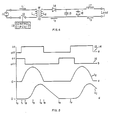
- Figure 5a illustrates the state of the switching device 12 and of the unidirectional conducting device 14 distinguishing between an "on" state in which the devices are in a conducting mode and an "off" state in which the devices are in a blocking mode;
- Figure 5b displays the on and off states of the unidirectional conducting device (16).
- the secondary current waveform, 1 2 (t) is sketched in Figure 5c; the voltage V c (t) across capacitor 15 is sketched in Figure 5d.
- the analysis begins at time t, when the control circuit 13 closes the switching device 12 setting it in a conducting mode. Voltage V in is then applied across the primary winding of the power transformer 10. The induced voltage across the secondary winding of transformer 10 forward biases the unidirectional conducting device 14 and the device begins to conduct a current l 2 (t). Because of the effective leakage inductance of transformer 10, this current 1 2 (t), as well as the primary current l 1 (t), has a finite rise time. In the following time interval between t, and t 2 , the rise of 1 2 is linear, as sketched in Figure 5c. In this interval, the voltage V c (t) across capacitor 15 remains zero (see Figure 5d), as the unidirectional conducting device 16 remains forward biased and conducts a current equal to the difference between the sink current 1 3 and the secondary current 1 2 .
- the secondary current equals the sink current. Then the device 16 smoothly becomes reverse biased and reverts to a blocking mode, as indicated in Figure 5b. In the following interval between t 2 and t 3 , the rise of the secondary current continues, but at a decreasing rate as the difference l 2 ⁇ l 3 begins to charge the capacitor 15 to a positive voltage V c (t) as sketched in Figure 5d.
- the voltage V c equals the transformed source voltage V in M/L.
- the secondary current reaches its peak value. In terms of an equivalent model, this is the time when the voltage across the effective leakage inductance changes sign. In the following time interval between t 3 and t 4 , the voltage V c (t) across the capacitor 15 continues to rise but at a decreasing rate, as the secondary current begins to fall.
- the secondary current 1 2 becomes smaller than the sink current 1 3 .
- the voltage V c (t) reaches its peak value 2V in . M/L i .
- the voltage V c (t) begins to fall, as the secondary current l 2 decreases at a faster rate.
- the unidirectional conducting device 15 becomes forward biased and begins to conduct the sink current l 3 .
- the sink current is conducted by the device 16, as the capacitor 15 remains discharged.
- the high frequency impedance of the effective leakage inductance lengthens the rise time of voltage and current waveforms eliminating turn-on switching losses, at the beginning of. the energy transfer cycle. Without the capacitor 15, this would be achieved at the expense of increased turn-off switching losses, as the amount of energy stored in the effective leakage inductance would grow with time.
- capacitor 15 will experience large ripple currents. This poses the problem of losses associated with the equivalent series resistance (ESR) of the capacitor, which would not be present in a forward converter. Thanks to the high operating frequencies, these losses may be kept negligible by a proper (and inexpensive) choice of capacitor type.
- ESR equivalent series resistance
- a possible choice is that of polypropylene or other film with very low high frequency dissipation factor in an extended foil construction. At frequencies of the order of several hundred kilohertz, the needed capacitance is small enough so that the size and cost of such a capacitor, in the scale set by the converter as a whole, are insignificant. Yet such as capacitor will exhibit ESR values as low as a few milliohms.
- V c (t) is "a priori" bounded between zero and twice the transforms source voltage, 2V in M/L 1 . If V c (t) is allowed to go negative, its peak positive value is no longer limited, as the capacitor 15 would then resonate with the effective leakage inductance of transformer 10. This would open up the possibility of run-away solutions and pose serious stability problems.
- the unidirectional conducting device 16 plays an important role in the new conversion topology.
- transformer 10 Equally important is the role of the transformer 10, with its multiplicity of functions, including isolation, voltage multiplication and provision for magnetic energy storage by its leakage inductance.
- the converter in Figure 4 can provide a regulated output voltage by a straight forward application of control mechanisms familiar to those skilled in the art. Not every approach to voltage regulation is however applicable. In particular, because of the inherent approximate quantization of the energy transferred in one cycle, the new topology does not lend itself to control techniques based on Pulse Width Modulation. With the duration of an energy transfer cycle approximately quantized, the control variable must then be the time interval between cycles. This interval can be made a continuous variable or a discrete - variable, i.e., an integer multiple of a fixed time interval.
- the control circuit 13 senses the voltage across the load. Under steady state conditions and assuming ideal circuit elements the time average of the voltage across inductor 17 vanishes and therefore the voltage across the load is equal to the average over time of the voltage across capacitor 15, V c (t). When restricted to an energy transfer cycle, such as the time interval between t 1 and t 5 in Figure 5, this average is equal-to the transformed source voltage: When restricted to a complementary time interval, such as the interval between t 5 and t 7 in Figure 5, the time average of V c (t) is less than the transformed source voltage, V c M/L), and approaches zero as the interval is increased. The transformed source voltage, V in M/L 1 , is therefore the maximum voltage which can in principle be sustained across the load. Lower voltages are obtained by spacing energy transfer cycles further apart.
- the control circuit 13 can be made to generate via a feedback loop a time interval which is continuously variable in response to the load to maintain a constant voltage across the load. With a fixed load the control circuit 13 will then initiate conduction by the switching device 12 periodically at times separated by that time interval. Under steady state conditions, this approach to voltage regulation leads to an optimal distribution of energy transfer cycles, each cycle being equally spaced from a neighboring cycle. This minimizes the ripple voltage across the load.
- control circuit 13 can incorporate a clock of fixed frequency and initiate conduction by the switching device 12 at times separated by a variable multiple integer of the clock's period, to maintain a constant voltage across the load. Since energy transfer cycles are not equally spaced from neighboring cycles, simple implementations of this approach exhibit higher ripple voltages as counterpart to a faster transient response.
Landscapes
- Engineering & Computer Science (AREA)
- Power Engineering (AREA)
- Dc-Dc Converters (AREA)
- Amplifiers (AREA)
- Control Of Motors That Do Not Use Commutators (AREA)
Claims (11)
Priority Applications (1)
| Application Number | Priority Date | Filing Date | Title |
|---|---|---|---|
| AT82901257T ATE36785T1 (de) | 1981-03-20 | 1982-03-19 | Bei nullstrom schaltender durchflussumrichter. |
Applications Claiming Priority (2)
| Application Number | Priority Date | Filing Date | Title |
|---|---|---|---|
| US246120 | 1981-03-20 | ||
| US06/246,120 US4415959A (en) | 1981-03-20 | 1981-03-20 | Forward converter switching at zero current |
Publications (3)
| Publication Number | Publication Date |
|---|---|
| EP0074399A1 EP0074399A1 (de) | 1983-03-23 |
| EP0074399A4 EP0074399A4 (de) | 1984-07-25 |
| EP0074399B1 true EP0074399B1 (de) | 1988-08-24 |
Family
ID=22929382
Family Applications (1)
| Application Number | Title | Priority Date | Filing Date |
|---|---|---|---|
| EP82901257A Expired EP0074399B1 (de) | 1981-03-20 | 1982-03-19 | Bei nullstrom schaltender durchflussumrichter |
Country Status (6)
| Country | Link |
|---|---|
| US (1) | US4415959A (de) |
| EP (1) | EP0074399B1 (de) |
| JP (1) | JPS58500585A (de) |
| AT (1) | ATE36785T1 (de) |
| DE (1) | DE3278961D1 (de) |
| WO (1) | WO1982003302A1 (de) |
Families Citing this family (142)
| Publication number | Priority date | Publication date | Assignee | Title |
|---|---|---|---|---|
| USRE36098E (en) * | 1982-02-04 | 1999-02-16 | Vlt Corporation | Optimal resetting of the transformer's core in single-ended forward converters |
| US4504895A (en) * | 1982-11-03 | 1985-03-12 | General Electric Company | Regulated dc-dc converter using a resonating transformer |
| US4628432A (en) * | 1984-05-29 | 1986-12-09 | Boschert Inc. | Proportional transistor base drive circuit for use in power converters |
| CA1236522A (en) * | 1984-08-07 | 1988-05-10 | Harald Stasch | Switched power supply comprising a free-running flow transformer without control loop |
| US4680687A (en) * | 1984-08-07 | 1987-07-14 | Siemens Aktiengesellschaft | Switch-mode power supply having a free-running forward converter |
| US4618919A (en) * | 1984-10-04 | 1986-10-21 | Sperry Corporation | Topology for miniature power supply with low voltage and low ripple requirements |
| US4648020A (en) * | 1985-02-26 | 1987-03-03 | Vicor Corporation | Power booster switching at zero current |
| US4675797A (en) * | 1985-11-06 | 1987-06-23 | Vicor Corporation | Current-fed, forward converter switching at zero current |
| US4688160A (en) * | 1985-12-19 | 1987-08-18 | American Telephone And Telegraph Co., At&T Bell Labs | Single ended forward converter with resonant commutation of magnetizing current |
| US4709316A (en) * | 1985-12-27 | 1987-11-24 | General Electric Company | Single-ended DC-to-DC converter with lossless switching |
| US4785387A (en) * | 1986-04-28 | 1988-11-15 | Virginia Tech Intellectual Properties, Inc. | Resonant converters with secondary-side resonance |
| US4736285A (en) * | 1986-06-19 | 1988-04-05 | Veeco Instruments, Inc. | Demagnetization circuit for forward converter |
| US4727308A (en) * | 1986-08-28 | 1988-02-23 | International Business Machines Corporation | FET power converter with reduced switching loss |
| FR2608857B1 (fr) * | 1986-12-19 | 1989-05-12 | Sodilec Sa | Convertisseur continu-continu du type " forward " a commutation a courant nul et a fonctionnement en courants bidirectionnels |
| US4823249A (en) * | 1987-04-27 | 1989-04-18 | American Telephone And Telegraph Company At&T Bell Laboratories | High-frequency resonant power converter |
| US4788634A (en) * | 1987-06-22 | 1988-11-29 | Massachusetts Institute Of Technology | Resonant forward converter |
| US4774649A (en) * | 1987-07-01 | 1988-09-27 | Power-One, Inc. | Integrated magnetic resonant power converter |
| US4922397A (en) * | 1988-02-16 | 1990-05-01 | Digital Equipment Corporation | Apparatus and method for a quasi-resonant DC to DC bridge converter |
| FR2627644B1 (fr) * | 1988-02-24 | 1991-05-03 | Europ Agence Spatiale | Convertisseur continu-continu, sans pertes de commutation, notamment pour alimentation continue haute frequence ou pour amplificateur a tube a ondes progressives |
| US4951186A (en) * | 1988-03-04 | 1990-08-21 | Siemens Aktiengesellschaft | Single-ended forward frequency converter with a transformer and a demagnetization means |
| FR2632134B1 (fr) * | 1988-05-26 | 1990-09-14 | Cachan Lesir Ecole Normale Sup | Procede de linearisation pour convertisseur continu-continu et dispositifs mettant en oeuvre ce procede |
| US4829232A (en) * | 1988-09-02 | 1989-05-09 | General Motors Corporation | Nonlinear resonant switch and converter |
| US4831507A (en) * | 1988-09-12 | 1989-05-16 | Reliance Comm/Tec Corporation | Frequency controlled preload |
| US5073849A (en) * | 1988-12-20 | 1991-12-17 | Power-One, Inc. | Resonant DC to DC converter switching at zero current |
| US4991075A (en) * | 1989-02-14 | 1991-02-05 | Mitsubishi Denki Kabushiki Kaisha | Low-switching loss DC-DC converter |
| US4945466A (en) * | 1989-02-22 | 1990-07-31 | Borland Walter G | Resonant switching converter |
| US5065301A (en) * | 1989-09-22 | 1991-11-12 | Yokogawa Electric Corporation | Switching power supply |
| US5027264A (en) * | 1989-09-29 | 1991-06-25 | Wisconsin Alumni Research Foundation | Power conversion apparatus for DC/DC conversion using dual active bridges |
| US5066900A (en) * | 1989-11-14 | 1991-11-19 | Computer Products, Inc. | Dc/dc converter switching at zero voltage |
| US4959764A (en) * | 1989-11-14 | 1990-09-25 | Computer Products, Inc. | DC/DC converter switching at zero voltage |
| CA2029209C (en) * | 1989-11-22 | 1999-07-27 | Patrizio Vinciarelli | Zero-current switching forward power conversion with controllable energy transfer |
| US5235502A (en) * | 1989-11-22 | 1993-08-10 | Vlt Corporation | Zero current switching forward power conversion apparatus and method with controllable energy transfer |
| US5038263A (en) * | 1990-01-03 | 1991-08-06 | Eg&G Power Systems, Inc. | Ripple current reduction circuit |
| US4980616A (en) * | 1990-01-26 | 1990-12-25 | Laboratory For Imaging Sciences, Inc. | Driver circuit for inductive elements such as CRT deflection coils |
| US5180964A (en) * | 1990-03-28 | 1993-01-19 | Ewing Gerald D | Zero-voltage switched FM-PWM converter |
| US5079686A (en) * | 1990-06-08 | 1992-01-07 | Vlt Corporation | Enhancement-mode zero-current switching converter |
| US5126931A (en) * | 1990-09-07 | 1992-06-30 | Itt Corporation | Fixed frequency single ended forward converter switching at zero voltage |
| US5231563A (en) * | 1990-09-07 | 1993-07-27 | Itt Corporation | Square wave converter having an improved zero voltage switching operation |
| US5088016A (en) * | 1990-09-17 | 1992-02-11 | Vlt Corporation | Voltage-compliant dc-dc converter module |
| US5321348A (en) * | 1991-03-08 | 1994-06-14 | Vlt Corporation | Boost switching power conversion |
| JP3311391B2 (ja) | 1991-09-13 | 2002-08-05 | ヴィエルティー コーポレーション | 漏洩インダクタンス低減トランス、これを用いた高周波回路及びパワーコンバータ並びにトランスにおける漏洩インダクタンスの低減方法 |
| US5177675A (en) * | 1991-10-16 | 1993-01-05 | Shindengen Archer Corp. | Zero voltage, zero current, resonant converter |
| US6107860A (en) * | 1991-12-11 | 2000-08-22 | Vlt Corporation | High efficiency floating gate driver circuit using leakage-inductance transformer |
| US5181170A (en) * | 1991-12-26 | 1993-01-19 | Wisconsin Alumni Research Foundation | High efficiency DC/DC current source converter |
| US5291385A (en) * | 1992-04-02 | 1994-03-01 | Vlt Corporation | Zero-current switching forward power converter operating in damped reverse boost mode |
| US5224025A (en) * | 1992-04-21 | 1993-06-29 | Wisconsin Alumni Research Foundation | Forward converter with two active switches and unity power factor capability |
| US5367247A (en) * | 1992-08-10 | 1994-11-22 | International Business Machines Corporation | Critically continuous boost converter |
| US5313145A (en) * | 1992-08-31 | 1994-05-17 | Francis Jr Ralph M | Power supply for a gas discharge device |
| JP3324151B2 (ja) * | 1992-09-22 | 2002-09-17 | 富士電機株式会社 | 直流電圧安定化電源装置 |
| US5434768A (en) * | 1993-02-12 | 1995-07-18 | Rompower | Fixed frequency converter switching at zero voltage |
| US5418709A (en) * | 1993-03-24 | 1995-05-23 | The United States Of America As Represented By The Administrator Of The National Aeronautics And Space Administration | Forback DC-to-DC converter |
| US5436820A (en) * | 1993-06-09 | 1995-07-25 | Eldec Corporation | Power converter with dual PWM control |
| US7236086B1 (en) | 1993-06-14 | 2007-06-26 | Vlt, Inc. | Power converter configuration, control, and construction |
| US5485362A (en) * | 1993-09-08 | 1996-01-16 | Eos Corporation | Resonant power converter for changing the magnitude of a DC voltage |
| JP2868422B2 (ja) * | 1993-10-28 | 1999-03-10 | ヴィエルティー コーポレーション | 電力変換における電流検出装置及び方法 |
| US5623397A (en) * | 1994-01-27 | 1997-04-22 | Vlt Corporation | Power conversion in anticipatory reverse boost mode |
| EP0676854B1 (de) * | 1994-04-08 | 2001-12-12 | Vlt Corporation | Effiziente Leistungsumwandlung |
| US5490057A (en) * | 1994-05-06 | 1996-02-06 | Vlt Corporation | Feedback control system having predictable open-loop gain |
| US5659460A (en) * | 1994-11-03 | 1997-08-19 | Vlt Corporation | Switch control in quantized power converters |
| JP2806283B2 (ja) * | 1994-12-12 | 1998-09-30 | ヤマハ株式会社 | スイッチング電源回路 |
| EP0723331B1 (de) | 1995-01-17 | 2003-05-07 | Vlt Corporation | Regelung der in den Transformatoren von Schaltnetzteilen gepseicherten Energie |
| US5694304A (en) * | 1995-02-03 | 1997-12-02 | Ericsson Raynet Corporation | High efficiency resonant switching converters |
| US5712772A (en) * | 1995-02-03 | 1998-01-27 | Ericsson Raynet | Controller for high efficiency resonant switching converters |
| US5499187A (en) * | 1995-04-03 | 1996-03-12 | Arinc Research Corporation | Voltage sensing, autoselecting aircraft power supply interface |
| US5663635A (en) * | 1995-05-24 | 1997-09-02 | Vlt Corporation | Reverse energy transfer in zero-current switching power conversion |
| EP0775765B1 (de) | 1995-11-27 | 2004-02-04 | Vlt Corporation | Plattierung von permeablen Kernen |
| US5684683A (en) * | 1996-02-09 | 1997-11-04 | Wisconsin Alumni Research Foundation | DC-to-DC power conversion with high current output |
| US5781419A (en) * | 1996-04-12 | 1998-07-14 | Soft Switching Technologies, Inc. | Soft switching DC-to-DC converter with coupled inductors |
| US5694309A (en) * | 1996-04-16 | 1997-12-02 | Vlt Corporation | Synchronization of power converter arrays |
| US5946210A (en) * | 1996-04-19 | 1999-08-31 | Vlt Corporation | Configuring power converters |
| US5724237A (en) * | 1996-06-11 | 1998-03-03 | Unipower Corporation | Apparatus and method for sharing a load current among frequency-controlled D.C.-to-D.C. converters |
| US5875104A (en) * | 1997-06-26 | 1999-02-23 | Vlt Corporation | Operating switching power converters in a phased power sharing array |
| US5838557A (en) * | 1997-07-28 | 1998-11-17 | Altor, Inc. | Circuit for use in a DC-DC converter having a booster module |
| US6110213A (en) | 1997-11-06 | 2000-08-29 | Vlt Coporation | Fabrication rules based automated design and manufacturing system and method |
| US5909362A (en) * | 1998-01-12 | 1999-06-01 | Eldec Corporation | Resonant power converter |
| US5920473A (en) * | 1998-03-09 | 1999-07-06 | Magnetic Technology, Inc. | Dc-to-Dc power converter with integrated magnetic power transformer |
| US6069801A (en) * | 1998-07-16 | 2000-05-30 | Vlt Corporation | Power factor correction in switching power conversion |
| US6490177B1 (en) | 1998-10-05 | 2002-12-03 | Salvador Figueroa | Resonant power converter with primary-side tuning and zero-current switching |
| US6243276B1 (en) | 1999-05-07 | 2001-06-05 | S-B Power Tool Company | Power supply system for battery operated devices |
| US6388853B1 (en) * | 1999-09-28 | 2002-05-14 | Power Integrations, Inc. | Method and apparatus providing final test and trimming for a power supply controller |
| US6442047B1 (en) | 1999-10-08 | 2002-08-27 | Lambda Electronics, Inc. | Power conversion apparatus and methods with reduced current and voltage switching |
| US6400579B2 (en) * | 2000-03-24 | 2002-06-04 | Slobodan Cuk | Lossless switching DC to DC converter with DC transformer |
| US6462962B1 (en) | 2000-09-08 | 2002-10-08 | Slobodan Cuk | Lossless switching DC-to-DC converter |
| US6809508B2 (en) * | 2000-10-20 | 2004-10-26 | Ethicon Endo-Surgery, Inc. | Detection circuitry for surgical handpiece system |
| KR100860397B1 (ko) | 2001-01-30 | 2008-09-26 | 트루 솔라 오토노미 홀딩 비.브이. | 전압 변환 회로 |
| US6794836B2 (en) * | 2001-02-06 | 2004-09-21 | Invacare Corporation | Electric motor drive controller with voltage control circuit operative in different modes |
| US6765987B2 (en) | 2001-03-15 | 2004-07-20 | Safe Food Technologies, Inc. | Resonant plasma x-ray source |
| US6522108B2 (en) | 2001-04-13 | 2003-02-18 | Vlt Corporation | Loss and noise reduction in power converters |
| US6768656B2 (en) * | 2002-01-28 | 2004-07-27 | Salvador Figueroa | Power converter with input-side resonance and pulse-position demodulation feedback control |
| US6771518B2 (en) | 2002-08-26 | 2004-08-03 | Potentia Semiconductor, Inc. | DC converters |
| JP4082248B2 (ja) * | 2003-03-12 | 2008-04-30 | 松下電工株式会社 | 電源装置及び放電灯点灯装置 |
| JP4256810B2 (ja) * | 2003-05-28 | 2009-04-22 | オーディオ・ラボ有限会社 | 逆起電力防止ユニット |
| US9153960B2 (en) | 2004-01-15 | 2015-10-06 | Comarco Wireless Technologies, Inc. | Power supply equipment utilizing interchangeable tips to provide power and a data signal to electronic devices |
| US20050162021A1 (en) * | 2004-01-26 | 2005-07-28 | Dell Products L.P. | Information handling system including zero voltage switching power supply |
| US7184279B2 (en) * | 2005-04-01 | 2007-02-27 | Thermatool Corp. | Solid state switching circuit |
| US8169185B2 (en) | 2006-01-31 | 2012-05-01 | Mojo Mobility, Inc. | System and method for inductive charging of portable devices |
| US11201500B2 (en) | 2006-01-31 | 2021-12-14 | Mojo Mobility, Inc. | Efficiencies and flexibilities in inductive (wireless) charging |
| US7952322B2 (en) | 2006-01-31 | 2011-05-31 | Mojo Mobility, Inc. | Inductive power source and charging system |
| US7738266B2 (en) * | 2006-05-26 | 2010-06-15 | Cambridge Semiconductor Limited | Forward power converter controllers |
| GB0610422D0 (en) * | 2006-05-26 | 2006-07-05 | Cambridge Semiconductor Ltd | Forward power converters |
| US7948208B2 (en) | 2006-06-01 | 2011-05-24 | Mojo Mobility, Inc. | Power source, charging system, and inductive receiver for mobile devices |
| US11329511B2 (en) | 2006-06-01 | 2022-05-10 | Mojo Mobility Inc. | Power source, charging system, and inductive receiver for mobile devices |
| GB2447874B (en) * | 2007-03-30 | 2009-07-29 | Cambridge Semiconductor Ltd | Forward power converter controllers |
| GB2455940B (en) | 2007-03-30 | 2010-11-24 | Cambridge Semiconductor Ltd | Forward power converter controllers |
| GB2447873B (en) * | 2007-03-30 | 2009-07-29 | Cambridge Semiconductor Ltd | Forward power converter controllers |
| US20090096565A1 (en) * | 2007-10-16 | 2009-04-16 | Comarco Wireless Technologies, Inc. | Parallel gapped ferrite core |
| KR101434604B1 (ko) * | 2008-03-03 | 2014-08-26 | 삼성전자주식회사 | 제로 전류 스위칭을 이용한 바이어스 모듈레이터 장치 및 방법 |
| US20110050164A1 (en) * | 2008-05-07 | 2011-03-03 | Afshin Partovi | System and methods for inductive charging, and improvements and uses thereof |
| WO2010009760A1 (en) * | 2008-07-22 | 2010-01-28 | Aps Electronic Ag | Multiphase soft-switched dc-dc converter |
| US9032880B2 (en) | 2009-01-23 | 2015-05-19 | Magnemotion, Inc. | Transport system powered by short block linear synchronous motors and switching mechanism |
| US8616134B2 (en) | 2009-01-23 | 2013-12-31 | Magnemotion, Inc. | Transport system powered by short block linear synchronous motors |
| US8967051B2 (en) * | 2009-01-23 | 2015-03-03 | Magnemotion, Inc. | Transport system powered by short block linear synchronous motors and switching mechanism |
| CN102870175B (zh) * | 2010-02-19 | 2014-06-04 | 王明亮 | 硅基功率电感 |
| US8890470B2 (en) | 2010-06-11 | 2014-11-18 | Mojo Mobility, Inc. | System for wireless power transfer that supports interoperability, and multi-pole magnets for use therewith |
| US11342777B2 (en) | 2011-01-18 | 2022-05-24 | Mojo Mobility, Inc. | Powering and/or charging with more than one protocol |
| US10115520B2 (en) | 2011-01-18 | 2018-10-30 | Mojo Mobility, Inc. | Systems and method for wireless power transfer |
| US9178369B2 (en) | 2011-01-18 | 2015-11-03 | Mojo Mobility, Inc. | Systems and methods for providing positioning freedom, and support of different voltages, protocols, and power levels in a wireless power system |
| US9496732B2 (en) | 2011-01-18 | 2016-11-15 | Mojo Mobility, Inc. | Systems and methods for wireless power transfer |
| CN108964442A (zh) | 2011-05-05 | 2018-12-07 | 北极砂技术有限公司 | 用于电源转换的装置 |
| US10680515B2 (en) | 2011-05-05 | 2020-06-09 | Psemi Corporation | Power converters with modular stages |
| KR101668925B1 (ko) | 2011-06-07 | 2016-10-24 | 마그네모션, 인코포레이티드 | 선형 동기 모터 추진 시스템의 다목적 제어 |
| US8743553B2 (en) | 2011-10-18 | 2014-06-03 | Arctic Sand Technologies, Inc. | Power converters with integrated capacitors |
| EP2748918B1 (de) | 2011-11-14 | 2015-03-04 | Cognipower, LLC | Getaktete verbundleistungswandler mit haupt- und zusatzreglern |
| RU2479100C1 (ru) * | 2011-12-07 | 2013-04-10 | Федеральное государственное унитарное предприятие "Научно-производственное объединение автоматики имени Н.А. Семихатова" | Источник питания |
| US8723491B2 (en) * | 2011-12-19 | 2014-05-13 | Arctic Sand Technologies, Inc. | Control of power converters with capacitive energy transfer |
| US20130271069A1 (en) | 2012-03-21 | 2013-10-17 | Mojo Mobility, Inc. | Systems and methods for wireless power transfer |
| US9722447B2 (en) | 2012-03-21 | 2017-08-01 | Mojo Mobility, Inc. | System and method for charging or powering devices, such as robots, electric vehicles, or other mobile devices or equipment |
| US9219421B2 (en) | 2012-10-09 | 2015-12-22 | Solantro Semiconductor Corp. | Forward boost power converters and methods |
| US9787179B1 (en) | 2013-03-11 | 2017-10-10 | Picor Corporation | Apparatus and methods for control of discontinuous-mode power converters |
| US8619445B1 (en) | 2013-03-15 | 2013-12-31 | Arctic Sand Technologies, Inc. | Protection of switched capacitor power converter |
| US8724353B1 (en) | 2013-03-15 | 2014-05-13 | Arctic Sand Technologies, Inc. | Efficient gate drivers for switched capacitor converters |
| US9837846B2 (en) | 2013-04-12 | 2017-12-05 | Mojo Mobility, Inc. | System and method for powering or charging receivers or devices having small surface areas or volumes |
| US9802507B2 (en) | 2013-09-21 | 2017-10-31 | Magnemotion, Inc. | Linear motor transport for packaging and other uses |
| DE102013223194A1 (de) * | 2013-11-14 | 2015-05-21 | Robert Bosch Gmbh | Gleichspannungswandler, Verfahren zum Takten eines Umformers eines Gleichspannungswandlers und Verfahren zum Wandeln von Gleichspannung |
| US9509221B2 (en) | 2013-12-18 | 2016-11-29 | Solantro Semiconductor Corp. | Forward boost power converters with tapped transformers and related methods |
| FR3020523B1 (fr) * | 2014-04-29 | 2016-05-06 | Valeo Systemes De Controle Moteur | Alimentation electrique et procede de commande d'une alimentation electrique |
| KR102688244B1 (ko) | 2015-03-13 | 2024-07-24 | 피세미 코포레이션 | 단열 커패시터 간 전하 수송을 용이하게 하기 위한 인덕터를 가지는 직류-직류 변압기 |
| CN108028600B (zh) | 2015-07-08 | 2022-03-08 | 派更半导体公司 | 开关电容器电力转换器 |
| CN105471254A (zh) * | 2016-02-01 | 2016-04-06 | 英麦科(厦门)微电子科技有限公司 | 一种直流-直流变换器 |
| US10773093B2 (en) | 2017-05-29 | 2020-09-15 | Elegant Mathematics LLC | Real-time methods for magnetic resonance spectra acquisition, imaging and non-invasive ablation |
| US11444485B2 (en) | 2019-02-05 | 2022-09-13 | Mojo Mobility, Inc. | Inductive charging system with charging electronics physically separated from charging coil |
| FR3123515A1 (fr) | 2021-06-01 | 2022-12-02 | Renault S.A.S | Système d’alimentation électrique d’au moins une machine électrique de traction d’un véhicule automobile alimentée par au moins deux sources de puissance. |
Family Cites Families (19)
| Publication number | Priority date | Publication date | Assignee | Title |
|---|---|---|---|---|
| US3259829A (en) * | 1961-07-25 | 1966-07-05 | Gen Electric | Resonant charging circuit capable of producing an output voltage which is higher than the input voltage |
| BE626463A (de) * | 1961-12-27 | |||
| US3385999A (en) * | 1965-09-14 | 1968-05-28 | Westinghouse Electric Corp | Discharge lamp transformer coil form having winding on insulated flange thereof |
| US3529228A (en) * | 1966-07-08 | 1970-09-15 | Union Carbide Corp | Low loss capacitor charging circuit |
| NL6708900A (de) * | 1967-06-27 | 1967-09-25 | ||
| GB1246860A (en) * | 1968-02-10 | 1971-09-22 | Wandel & Goltermann | Direct current converter |
| US3621362A (en) * | 1969-03-26 | 1971-11-16 | Nasa | Load-insensitive electrical device |
| US3663940A (en) * | 1970-05-21 | 1972-05-16 | Nasa | Controllable, load insensitive power converters |
| DE2260042A1 (de) * | 1972-01-05 | 1973-07-19 | Zentronik Veb K | Stellglied fuer eine stabilisierungsschaltung mit getasteter regelung |
| DE2218055A1 (de) * | 1972-04-14 | 1973-10-31 | Schoppe & Faeser Gmbh | Schaltungsanordnung zur konstanthaltung einer gleichspannung |
| US3953779A (en) * | 1974-05-30 | 1976-04-27 | Francisc Carol Schwarz | Electronic control system for efficient transfer of power through resonant circuits |
| US4007413A (en) * | 1975-12-08 | 1977-02-08 | Bell Telephone Laboratories, Incorporated | Converter utilizing leakage inductance to control energy flow and improve signal waveforms |
| US4138715A (en) * | 1976-01-28 | 1979-02-06 | Martin Marietta Corporation | Resonant switching converter |
| US4017784A (en) * | 1976-05-17 | 1977-04-12 | Litton Systems, Inc. | DC to DC converter |
| US4024453A (en) * | 1976-08-26 | 1977-05-17 | General Motors Corporation | Inverter for supplying a regulated voltage |
| JPS5378042A (en) * | 1976-12-20 | 1978-07-11 | Sanyo Electric Co Ltd | Switching control type power source circuit |
| IT1069949B (it) * | 1976-12-22 | 1985-03-25 | Ciro Pieri Di | Inverters a tiristori per riscaldamento ad induzione con alimentazione peroidica del circuito risonante mediante impulsi costanti di energia |
| US4158881A (en) * | 1978-06-12 | 1979-06-19 | Litton Systems, Inc. | DC to DC converter |
| US4318164A (en) * | 1979-03-15 | 1982-03-02 | Tokyo Shibaura Denki Kabushiki Kaisha | High frequency switching circuit having preselected parameters to reduce power dissipation therein |
-
1981
- 1981-03-20 US US06/246,120 patent/US4415959A/en not_active Expired - Lifetime
-
1982
- 1982-03-19 DE DE8282901257T patent/DE3278961D1/de not_active Expired
- 1982-03-19 AT AT82901257T patent/ATE36785T1/de not_active IP Right Cessation
- 1982-03-19 JP JP57501280A patent/JPS58500585A/ja active Granted
- 1982-03-19 EP EP82901257A patent/EP0074399B1/de not_active Expired
- 1982-03-19 WO PCT/US1982/000342 patent/WO1982003302A1/en not_active Ceased
Also Published As
| Publication number | Publication date |
|---|---|
| DE3278961D1 (en) | 1988-09-29 |
| WO1982003302A1 (en) | 1982-09-30 |
| US4415959A (en) | 1983-11-15 |
| EP0074399A1 (de) | 1983-03-23 |
| JPS58500585A (ja) | 1983-04-14 |
| ATE36785T1 (de) | 1988-09-15 |
| EP0074399A4 (de) | 1984-07-25 |
| JPH0247196B2 (de) | 1990-10-18 |
Similar Documents
| Publication | Publication Date | Title |
|---|---|---|
| US4415959A (en) | Forward converter switching at zero current | |
| US5126931A (en) | Fixed frequency single ended forward converter switching at zero voltage | |
| US5991171A (en) | DC-to-DC converters | |
| US6198260B1 (en) | Zero voltage switching active reset power converters | |
| EP0123147B1 (de) | Geregelter Gleichspannungswandler | |
| EP0744817B1 (de) | Energierückübertragung in einer nullstromschaltenden Leistungswandlerschaltung | |
| US5097196A (en) | Zero-voltage-switched multiresonant DC to DC converter | |
| US5999433A (en) | Half-bridge DC to DC converter with low output current ripple | |
| CN114499146B (zh) | 一种适用于谐振变换器的闭环软启动控制系统 | |
| US4720668A (en) | Zero-voltage switching quasi-resonant converters | |
| US4855888A (en) | Constant frequency resonant power converter with zero voltage switching | |
| EP0508595B1 (de) | Spannungserhöhende Schaltleistungswandlung | |
| US5880940A (en) | Low cost high efficiency power converter | |
| US4720667A (en) | Zero-current switching quasi-resonant converters operating in a full-wave mode | |
| US5291382A (en) | Pulse width modulated DC/DC converter with reduced ripple current coponent stress and zero voltage switching capability | |
| EP0723331B1 (de) | Regelung der in den Transformatoren von Schaltnetzteilen gepseicherten Energie | |
| EP0490639B1 (de) | Schaltenergiequelle | |
| US7778046B1 (en) | Voltage step-up switching DC-to-DC converter field of the invention | |
| US5274539A (en) | Capacitance-multiplying converters for supplying distributed pulsed loads | |
| EP0564289B1 (de) | Nullstromschaltender Durchflusswandler | |
| EP3994541A1 (de) | Selbsteinstellende strominjektionstechnologie | |
| Harada et al. | Non-resonant converter for megahertz switching | |
| Xi et al. | A zero voltage switching flyback converter topology | |
| JP2996014B2 (ja) | Dc−dcコンバータ | |
| Harada et al. | Saturable inductor commutation for zero voltage switching in DC-DC converter |
Legal Events
| Date | Code | Title | Description |
|---|---|---|---|
| PUAI | Public reference made under article 153(3) epc to a published international application that has entered the european phase |
Free format text: ORIGINAL CODE: 0009012 |
|
| 17P | Request for examination filed |
Effective date: 19821124 |
|
| AK | Designated contracting states |
Designated state(s): AT BE CH DE FR GB LI LU NL SE |
|
| RAP1 | Party data changed (applicant data changed or rights of an application transferred) |
Owner name: VICOR CORPORATION |
|
| GRAA | (expected) grant |
Free format text: ORIGINAL CODE: 0009210 |
|
| AK | Designated contracting states |
Kind code of ref document: B1 Designated state(s): AT BE CH DE FR GB LI LU NL SE |
|
| REF | Corresponds to: |
Ref document number: 36785 Country of ref document: AT Date of ref document: 19880915 Kind code of ref document: T |
|
| REF | Corresponds to: |
Ref document number: 3278961 Country of ref document: DE Date of ref document: 19880929 |
|
| ET | Fr: translation filed | ||
| PLBE | No opposition filed within time limit |
Free format text: ORIGINAL CODE: 0009261 |
|
| STAA | Information on the status of an ep patent application or granted ep patent |
Free format text: STATUS: NO OPPOSITION FILED WITHIN TIME LIMIT |
|
| 26N | No opposition filed | ||
| EPTA | Lu: last paid annual fee | ||
| EAL | Se: european patent in force in sweden |
Ref document number: 82901257.4 |
|
| PGFP | Annual fee paid to national office [announced via postgrant information from national office to epo] |
Ref country code: FR Payment date: 20010302 Year of fee payment: 20 |
|
| PGFP | Annual fee paid to national office [announced via postgrant information from national office to epo] |
Ref country code: CH Payment date: 20010305 Year of fee payment: 20 |
|
| PGFP | Annual fee paid to national office [announced via postgrant information from national office to epo] |
Ref country code: SE Payment date: 20010306 Year of fee payment: 20 Ref country code: GB Payment date: 20010306 Year of fee payment: 20 Ref country code: AT Payment date: 20010306 Year of fee payment: 20 |
|
| PGFP | Annual fee paid to national office [announced via postgrant information from national office to epo] |
Ref country code: NL Payment date: 20010307 Year of fee payment: 20 Ref country code: DE Payment date: 20010307 Year of fee payment: 20 |
|
| PGFP | Annual fee paid to national office [announced via postgrant information from national office to epo] |
Ref country code: LU Payment date: 20010313 Year of fee payment: 20 |
|
| PGFP | Annual fee paid to national office [announced via postgrant information from national office to epo] |
Ref country code: BE Payment date: 20010410 Year of fee payment: 20 |
|
| BE20 | Be: patent expired |
Free format text: 20020319 *VICOR CORP. |
|
| REG | Reference to a national code |
Ref country code: GB Ref legal event code: IF02 |
|
| PG25 | Lapsed in a contracting state [announced via postgrant information from national office to epo] |
Ref country code: LI Free format text: LAPSE BECAUSE OF EXPIRATION OF PROTECTION Effective date: 20020318 Ref country code: GB Free format text: LAPSE BECAUSE OF EXPIRATION OF PROTECTION Effective date: 20020318 Ref country code: CH Free format text: LAPSE BECAUSE OF EXPIRATION OF PROTECTION Effective date: 20020318 |
|
| PG25 | Lapsed in a contracting state [announced via postgrant information from national office to epo] |
Ref country code: NL Free format text: LAPSE BECAUSE OF EXPIRATION OF PROTECTION Effective date: 20020319 Ref country code: LU Free format text: LAPSE BECAUSE OF EXPIRATION OF PROTECTION Effective date: 20020319 Ref country code: AT Free format text: LAPSE BECAUSE OF EXPIRATION OF PROTECTION Effective date: 20020319 |
|
| REG | Reference to a national code |
Ref country code: GB Ref legal event code: PE20 Effective date: 20020318 |
|
| REG | Reference to a national code |
Ref country code: CH Ref legal event code: PL |
|
| EUG | Se: european patent has lapsed |
Ref document number: 82901257.4 |
|
| NLV7 | Nl: ceased due to reaching the maximum lifetime of a patent |
Effective date: 20020319 |
|
| NLV7 | Nl: ceased due to reaching the maximum lifetime of a patent |
Effective date: 20020319 |