EP0075833A2 - Capteur de température à sémi-conducteur - Google Patents
Capteur de température à sémi-conducteur Download PDFInfo
- Publication number
- EP0075833A2 EP0075833A2 EP82108689A EP82108689A EP0075833A2 EP 0075833 A2 EP0075833 A2 EP 0075833A2 EP 82108689 A EP82108689 A EP 82108689A EP 82108689 A EP82108689 A EP 82108689A EP 0075833 A2 EP0075833 A2 EP 0075833A2
- Authority
- EP
- European Patent Office
- Prior art keywords
- temperature sensor
- semiconductor layer
- substrate
- sensor according
- semiconductor
- Prior art date
- Legal status (The legal status is an assumption and is not a legal conclusion. Google has not performed a legal analysis and makes no representation as to the accuracy of the status listed.)
- Withdrawn
Links
- 239000004065 semiconductor Substances 0.000 claims abstract description 38
- 239000000758 substrate Substances 0.000 claims abstract description 21
- 229910052710 silicon Inorganic materials 0.000 claims description 14
- 239000010703 silicon Substances 0.000 claims description 14
- 238000004544 sputter deposition Methods 0.000 claims description 6
- 238000000034 method Methods 0.000 claims description 5
- 238000002161 passivation Methods 0.000 claims description 4
- 238000000151 deposition Methods 0.000 claims description 3
- 230000008021 deposition Effects 0.000 claims description 3
- 239000000126 substance Substances 0.000 claims description 3
- 238000007740 vapor deposition Methods 0.000 claims description 3
- 238000005229 chemical vapour deposition Methods 0.000 claims description 2
- 239000000463 material Substances 0.000 claims description 2
- 230000006378 damage Effects 0.000 claims 1
- 238000004519 manufacturing process Methods 0.000 claims 1
- XUIMIQQOPSSXEZ-UHFFFAOYSA-N Silicon Chemical compound [Si] XUIMIQQOPSSXEZ-UHFFFAOYSA-N 0.000 description 12
- 239000002184 metal Substances 0.000 description 5
- VYPSYNLAJGMNEJ-UHFFFAOYSA-N Silicium dioxide Chemical compound O=[Si]=O VYPSYNLAJGMNEJ-UHFFFAOYSA-N 0.000 description 4
- 238000005516 engineering process Methods 0.000 description 2
- 235000012239 silicon dioxide Nutrition 0.000 description 2
- 239000000377 silicon dioxide Substances 0.000 description 2
- 101100008049 Caenorhabditis elegans cut-5 gene Proteins 0.000 description 1
- 239000011248 coating agent Substances 0.000 description 1
- 238000000576 coating method Methods 0.000 description 1
- 230000001419 dependent effect Effects 0.000 description 1
- 238000009792 diffusion process Methods 0.000 description 1
- 238000005530 etching Methods 0.000 description 1
- 238000002513 implantation Methods 0.000 description 1
- 238000005259 measurement Methods 0.000 description 1
- 230000000149 penetrating effect Effects 0.000 description 1
- 229920002120 photoresistant polymer Polymers 0.000 description 1
- 150000003376 silicon Chemical class 0.000 description 1
- 238000009966 trimming Methods 0.000 description 1
Images
Classifications
-
- G—PHYSICS
- G01—MEASURING; TESTING
- G01K—MEASURING TEMPERATURE; MEASURING QUANTITY OF HEAT; THERMALLY-SENSITIVE ELEMENTS NOT OTHERWISE PROVIDED FOR
- G01K7/00—Measuring temperature based on the use of electric or magnetic elements directly sensitive to heat ; Power supply therefor, e.g. using thermoelectric elements
- G01K7/16—Measuring temperature based on the use of electric or magnetic elements directly sensitive to heat ; Power supply therefor, e.g. using thermoelectric elements using resistive elements
- G01K7/22—Measuring temperature based on the use of electric or magnetic elements directly sensitive to heat ; Power supply therefor, e.g. using thermoelectric elements using resistive elements the element being a non-linear resistance, e.g. thermistor
- G01K7/223—Measuring temperature based on the use of electric or magnetic elements directly sensitive to heat ; Power supply therefor, e.g. using thermoelectric elements using resistive elements the element being a non-linear resistance, e.g. thermistor characterised by the shape of the resistive element
Definitions
- the invention relates to a temperature sensor with a semiconductor body as a measuring resistor, which is provided at its two ends with at least one contact electrode, so that the temperature can be determined from the resistance value of the semiconductor body.
- a temperature sensor made of a semiconductor body which on the one hand has an insulating layer on its top, in which a window is provided through which the semiconductor body is provided with a metal contact, and on the other hand on its top facing surface has a metal coating.
- at least one further window is provided, through which another metal contact contacts the semiconductor body contact, so as to make the propagation resistance between the metal contacts and the metal surface dependent or symmetrical depending on the current direction. This enables a temperature sensor without the current directional dependence of the resistance value.
- a silicon substrate without a pn junction is used for the measuring resistor for the semiconductor body.
- the desired accuracy is achieved through selective measurements, as a subsequent one Setting or trimming the nominal resistance value is not possible.
- a higher accuracy of the individual temperature sensors can therefore only be achieved through a lower yield.
- the range of use of such temperature sensors is limited to temperatures below approximately 150 ° C. by the self-conduction of the silicon substrate.
- the semiconductor body is designed as a layer which is arranged on a substrate.
- the substrate can consist of semiconductor material and contain, for example, an integrated circuit.
- An insulating layer is then provided between the substrate and the semiconductor layer.
- the semiconductor layer can consist of amorphous, polycrystalline or recrystallized silicon.
- the semiconductor layer can be applied to the substrate or the insulating layer by vapor deposition, sputtering, deposition in a glow discharge or by chemical vapor shutdown, this semiconductor layer then being partially removed in order to isolate the temperature-sensitive part of the temperature sensor from the surroundings. This partial removal of the semiconductor layer can take place wet or dry chemical or by means of sputtering.
- the semiconductor layer can be destroyed locally by the action of a laser beam, the laser incision being made by simultaneously measuring the resistance of the temperature rature sensor is controlled. This ensures that the nominal value of the temperature sensor is set by laser adjustment. In this way, high accuracies (deviations below 0.1%) can be achieved without reducing the yield as in the readout process.
- a so-called “horizontal arrangement” or a “vertical arrangement” is possible for the temperature sensor.
- the two electrodes are located at the two ends of the semiconductor layer parallel to the surface of the substrate, while in the vertical arrangement the two contact electrodes are provided at the two ends of the semiconductor layer perpendicular to the surface of the substrate.
- a contact electrode is provided between the insulating layer and the semiconductor layer.
- a passivation layer can also be applied to the semiconductor layer and the contact electrodes, which in turn applies in particular to the case mentioned first.
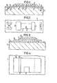
- a silicon dioxide layer 1 is provided on a silicon substrate 6, in which windows 10 are introduced by the usual photoresist and etching technology. Zones 11, which have a doping opposite to the silicon substrate 6, are introduced through these windows 10 by diffusion or implantation. If the silicon substrate is n-doped, for example, then these zones 11 are p-doped. The zones 11 form an integrated circuit in the silicon substrate 6.
- a silicon layer 3 is applied to the silicon dioxide layer 1 by vapor deposition, sputtering, deposition in a glow discharge or by chemical vapor deposition Method or brought by sputtering, so as to isolate the resistance to be produced from the environment. This silicon layer 3 is provided with contact electrodes 2, 8, which together with the silicon layer 3 form the temperature sensor.
- this is locally by a laser. cut 5 destroyed, so that the resistance between the contact electrodes 2 and 8 takes the desired value.
- the laser beam penetrating the laser incision 5 is expediently controlled while simultaneously measuring the resistance value between the contact electrodes 2 and 8. For example, the action of the laser beam can be switched off when this resistance takes the desired value.
- FIGS. 3 and 4 show a vertical arrangement.
- the silicon layer 3 lies between a lower contact electrode 9 and an upper contact electrode 13.
- the laser incision 5 is preferred with a larger area take, since the contact electrodes 9 and 13 are spaced only over the relatively thin silicon layer 3 and are thus separated from each other only by a relatively small resistance.
- the entire arrangement can also be covered by a passivation layer 4, as shown in FIG. 1.
Landscapes
- Physics & Mathematics (AREA)
- Nonlinear Science (AREA)
- General Physics & Mathematics (AREA)
- Semiconductor Integrated Circuits (AREA)
- Electrical Discharge Machining, Electrochemical Machining, And Combined Machining (AREA)
- Glass Compositions (AREA)
- Thermistors And Varistors (AREA)
- Measuring Temperature Or Quantity Of Heat (AREA)
Applications Claiming Priority (2)
| Application Number | Priority Date | Filing Date | Title |
|---|---|---|---|
| DE3138535 | 1981-09-28 | ||
| DE3138535A DE3138535A1 (de) | 1981-09-28 | 1981-09-28 | Temperatursensor mit einem halbleiterkoerper |
Publications (2)
| Publication Number | Publication Date |
|---|---|
| EP0075833A2 true EP0075833A2 (fr) | 1983-04-06 |
| EP0075833A3 EP0075833A3 (fr) | 1983-11-30 |
Family
ID=6142800
Family Applications (1)
| Application Number | Title | Priority Date | Filing Date |
|---|---|---|---|
| EP82108689A Withdrawn EP0075833A3 (fr) | 1981-09-28 | 1982-09-20 | Capteur de température à sémi-conducteur |
Country Status (3)
| Country | Link |
|---|---|
| EP (1) | EP0075833A3 (fr) |
| JP (1) | JPS5870588A (fr) |
| DE (1) | DE3138535A1 (fr) |
Cited By (3)
| Publication number | Priority date | Publication date | Assignee | Title |
|---|---|---|---|---|
| US4760434A (en) * | 1985-11-29 | 1988-07-26 | Nippondenso Co., Ltd. | Semiconductor device with protective means against overheating |
| GB2232253A (en) * | 1989-05-23 | 1990-12-05 | Samsung Electronics Co Ltd | Semiconductor temperature detecting circuit |
| US5136348A (en) * | 1986-10-08 | 1992-08-04 | Nippondenso Co., Ltd. | Structure and manufacturing method for thin-film semiconductor diode device |
Families Citing this family (4)
| Publication number | Priority date | Publication date | Assignee | Title |
|---|---|---|---|---|
| JPH0733979B2 (ja) * | 1984-07-31 | 1995-04-12 | 光照 木村 | 温度センサ |
| JPS62267629A (ja) * | 1986-05-16 | 1987-11-20 | Japan Atom Energy Res Inst | 高磁場領域における極低温計測用温度計 |
| DE4202733C2 (de) * | 1992-01-31 | 1995-06-08 | Bosch Gmbh Robert | Temperatursensor |
| JP2701824B2 (ja) * | 1996-02-09 | 1998-01-21 | 株式会社デンソー | 半導体装置 |
Family Cites Families (5)
| Publication number | Priority date | Publication date | Assignee | Title |
|---|---|---|---|---|
| US4276535A (en) * | 1977-08-23 | 1981-06-30 | Matsushita Electric Industrial Co., Ltd. | Thermistor |
| US4225877A (en) * | 1978-09-05 | 1980-09-30 | Sprague Electric Company | Integrated circuit with C-Mos logic, and a bipolar driver with polysilicon resistors |
| US4236298A (en) * | 1979-01-25 | 1980-12-02 | Milton Schonberger | Method of trimming thermistor or other electrical components and the contacts thereof |
| DE2965814D1 (en) * | 1979-03-21 | 1983-08-11 | Bbc Brown Boveri & Cie | Thin film resistor having a high temperature coefficient and method of manufacturing the same |
| EP0060427B1 (fr) * | 1981-03-16 | 1987-08-12 | Hanno Prof. Dr.-Ing. Schaumburg | Elément sensible pour la mesure de dimensions physiques ainsi que procédé pour sa fabrication et son utilisation |
-
1981
- 1981-09-28 DE DE3138535A patent/DE3138535A1/de not_active Withdrawn
-
1982
- 1982-09-20 EP EP82108689A patent/EP0075833A3/fr not_active Withdrawn
- 1982-09-24 JP JP57166400A patent/JPS5870588A/ja active Pending
Cited By (5)
| Publication number | Priority date | Publication date | Assignee | Title |
|---|---|---|---|---|
| US4760434A (en) * | 1985-11-29 | 1988-07-26 | Nippondenso Co., Ltd. | Semiconductor device with protective means against overheating |
| US4896199A (en) * | 1985-11-29 | 1990-01-23 | Nippondenso Co., Ltd. | Semiconductor device with protective means against overheating |
| US5136348A (en) * | 1986-10-08 | 1992-08-04 | Nippondenso Co., Ltd. | Structure and manufacturing method for thin-film semiconductor diode device |
| GB2232253A (en) * | 1989-05-23 | 1990-12-05 | Samsung Electronics Co Ltd | Semiconductor temperature detecting circuit |
| GB2232253B (en) * | 1989-05-23 | 1994-02-02 | Samsung Electronics Co Ltd | Semiconductor temperature detecting circuit |
Also Published As
| Publication number | Publication date |
|---|---|
| DE3138535A1 (de) | 1983-04-07 |
| JPS5870588A (ja) | 1983-04-27 |
| EP0075833A3 (fr) | 1983-11-30 |
Similar Documents
| Publication | Publication Date | Title |
|---|---|---|
| DE2732184C2 (de) | Verfahren zur Herstellung einer Halbleitervorrichtung | |
| DE69113579T2 (de) | Verfahren zur Herstellung einer DRAM-Zelle mit Stapelkondensator. | |
| EP0123309B1 (fr) | Procédé pour fabriquer des contacts stables à basse résistance dans des circuits semi-conducteurs intégrés | |
| DE2160427C3 (fr) | ||
| DE4219319A1 (de) | Mos-fet und herstellungsverfahren dafuer | |
| DE3603470A1 (de) | Verfahren zur herstellung von feldeffektbauelementen auf einem siliziumsubstrat | |
| DE3233568A1 (de) | Feldeffekttransistor und verfahren zum herstellen desselben | |
| EP0012220A1 (fr) | Procédé de fabrication d'un contact Schottky à anneau de garde auto-aligné | |
| DE2749607B2 (de) | Halbleiteranordnung und Verfahren zu deren Herstellung | |
| DE2425185A1 (de) | Verfahren zum herstellen einer halbleitervorrichtung | |
| DE3109074C2 (fr) | ||
| EP0129045A1 (fr) | Procédé de fabrication d'un transistor à effet de champ intégré ayant une couche isolante avec des contacts auto-alignés par rapport à l'électrode de grille | |
| DE2705468A1 (de) | Verfahren zur herstellung von transistoren durch ionenimplantation | |
| DE1464395C3 (de) | Feldeffekt-Transistor | |
| EP0000545A1 (fr) | Procédé de fabrication d'un dispositif semiconducteur à auto-alignement | |
| DE1514359B1 (de) | Feldeffekt-Halbleiterbauelement und Verfahren zu seiner Herstellung | |
| EP0075833A2 (fr) | Capteur de température à sémi-conducteur | |
| DE19637277A1 (de) | Widerstand für eine integrierte Schaltung | |
| DE2916732C2 (de) | Verfahren zum Herstellen von integrierten Halbleiterschaltungsanordnungen, bei dem Widerstandselemente gebildet werden | |
| DE2904480B2 (de) | Integrierte Halbleiterschaltung und Verfahren zu ihrem Herstellen | |
| DE2953394T1 (de) | Dielectrically-isolated integrated circuit complementary transistors for high voltage use | |
| DE2252868A1 (de) | Feldeffekttransistor mit zwei steuerelektroden fuer betrieb bei sehr hohen frequenzen | |
| DE3430941C2 (de) | Chemisch empfindlicher Feldeffekttransistor-Sensor | |
| DE69025784T2 (de) | Nichtflüchtige Speicher-Halbleiteranordnung | |
| DE3445775A1 (de) | Kapazitiver halbleiterdruckaufnehmer |
Legal Events
| Date | Code | Title | Description |
|---|---|---|---|
| PUAI | Public reference made under article 153(3) epc to a published international application that has entered the european phase |
Free format text: ORIGINAL CODE: 0009012 |
|
| AK | Designated contracting states |
Designated state(s): FR GB NL |
|
| PUAL | Search report despatched |
Free format text: ORIGINAL CODE: 0009013 |
|
| AK | Designated contracting states |
Designated state(s): FR GB NL |
|
| 17P | Request for examination filed |
Effective date: 19840524 |
|
| STAA | Information on the status of an ep patent application or granted ep patent |
Free format text: STATUS: THE APPLICATION IS DEEMED TO BE WITHDRAWN |
|
| 18D | Application deemed to be withdrawn |
Effective date: 19880930 |
|
| APAF | Appeal reference modified |
Free format text: ORIGINAL CODE: EPIDOSCREFNE |
|
| RIN1 | Information on inventor provided before grant (corrected) |
Inventor name: MITLEHNER, HEINZ, DR. RER. NAT. Inventor name: TOMASI, GILBERT, DR.-ING. |