EP0076495A2 - Fotodiode - Google Patents
Fotodiode Download PDFInfo
- Publication number
- EP0076495A2 EP0076495A2 EP82109103A EP82109103A EP0076495A2 EP 0076495 A2 EP0076495 A2 EP 0076495A2 EP 82109103 A EP82109103 A EP 82109103A EP 82109103 A EP82109103 A EP 82109103A EP 0076495 A2 EP0076495 A2 EP 0076495A2
- Authority
- EP
- European Patent Office
- Prior art keywords
- semiconductor layer
- layer
- semiconductor
- junction
- conductivity type
- Prior art date
- Legal status (The legal status is an assumption and is not a legal conclusion. Google has not performed a legal analysis and makes no representation as to the accuracy of the status listed.)
- Granted
Links
Images

Classifications
-
- H—ELECTRICITY
- H10—SEMICONDUCTOR DEVICES; ELECTRIC SOLID-STATE DEVICES NOT OTHERWISE PROVIDED FOR
- H10F—INORGANIC SEMICONDUCTOR DEVICES SENSITIVE TO INFRARED RADIATION, LIGHT, ELECTROMAGNETIC RADIATION OF SHORTER WAVELENGTH OR CORPUSCULAR RADIATION
- H10F99/00—Subject matter not provided for in other groups of this subclass
-
- H—ELECTRICITY
- H10—SEMICONDUCTOR DEVICES; ELECTRIC SOLID-STATE DEVICES NOT OTHERWISE PROVIDED FOR
- H10F—INORGANIC SEMICONDUCTOR DEVICES SENSITIVE TO INFRARED RADIATION, LIGHT, ELECTROMAGNETIC RADIATION OF SHORTER WAVELENGTH OR CORPUSCULAR RADIATION
- H10F30/00—Individual radiation-sensitive semiconductor devices in which radiation controls the flow of current through the devices, e.g. photodetectors
- H10F30/20—Individual radiation-sensitive semiconductor devices in which radiation controls the flow of current through the devices, e.g. photodetectors the devices having potential barriers, e.g. phototransistors
- H10F30/21—Individual radiation-sensitive semiconductor devices in which radiation controls the flow of current through the devices, e.g. photodetectors the devices having potential barriers, e.g. phototransistors the devices being sensitive to infrared, visible or ultraviolet radiation
- H10F30/22—Individual radiation-sensitive semiconductor devices in which radiation controls the flow of current through the devices, e.g. photodetectors the devices having potential barriers, e.g. phototransistors the devices being sensitive to infrared, visible or ultraviolet radiation the devices having only one potential barrier, e.g. photodiodes
- H10F30/225—Individual radiation-sensitive semiconductor devices in which radiation controls the flow of current through the devices, e.g. photodetectors the devices having potential barriers, e.g. phototransistors the devices being sensitive to infrared, visible or ultraviolet radiation the devices having only one potential barrier, e.g. photodiodes the potential barrier working in avalanche mode, e.g. avalanche photodiodes
- H10F30/2255—Individual radiation-sensitive semiconductor devices in which radiation controls the flow of current through the devices, e.g. photodetectors the devices having potential barriers, e.g. phototransistors the devices being sensitive to infrared, visible or ultraviolet radiation the devices having only one potential barrier, e.g. photodiodes the potential barrier working in avalanche mode, e.g. avalanche photodiodes in which the active layers form heterostructures, e.g. SAM structures
Definitions
- the present invention relates to a photo-detective semiconductor device which is reverse-biased in operation.
- the device of the specified type is usually called a photodiode or an avalanche photodiode.
- the photodiode or the avalanche photodiode is important as a photodetector in an optical communication system.
- Semiconductor lasers are used as light sources in the optical communication system. Regarding oscillation wavelengths of 0.8 pm - 1.4 pm, the semiconductor lasers of, e. g., the GaAs - GaAlAs and InGaAsP - InP systems are mainly employed.
- photodetectors for these semiconductor lasers ones made of a single crystal of Si are well known. However, they do not have a satisfactory sensitivity to light having wavelengths of and above 1 ⁇ m.
- a photodetector for the optical communication one employing a group III-V compound semiconductor material is required. With the compound semiconductor material, however, it is the present situation that a satisfactory operation cannot be achieved because of, particularly, underdeveloped surface passivation technology.
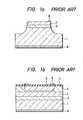
- Photosensors of mesa and planar structures as shown in Figures 1a and 1b are typical examples having hitherto been proposed.
- a semiconductor layer 2 of a first conductivity type and a semiconductor layer 3 of a second conductivity type are formed on a semiconductor substrate 1, and electrodes 8 and 9 are further disposed.
- the mesa structure in Figure 1a is undesirable in practical use in that, since a high electric field is exposed to the end face of a junction, the characteristics of the device are affected by the properties of a surface protective film.
- the planar structure in Figure 1b (for example, Japanese Laid-open Patent Application No. 55-132079) is expected to attain a stable operation as compared with the operation of the mesa structure.
- an n +- type InP layer 2 an InGaAsP layer 3 and an n-type InP layer 4 are formed on an InP semiconductor substrate 1.
- Shown at numeral 6 is a diffused layer of, e. g., Cd, the diffusion end face of which forms a p-n junction.
- Numeral 7 designates an insulating layer, and numerals 8 and 9 designate electrodes.
- the present invention provides a photo-detective semiconductor device which is high in sensitivity and low in dark current, and for which a fast operation is satisfactorily ensured.
- the present invention eliminates such disadvantage.
- the structure of the present invention consists in a photo-detective semiconductor device having, on a predetermined semiconductor substrate, at least a first semiconductor layer which exhibits a first conductivity type, a second semiconductor layer which is disposed on said first semiconductor layer, which has a forbidden band gap greater than that of said first semiconductor layer and which exhibits the first conductivity type, and a p-n junction which is formed by a region disposed in said second semiconductor layer and exhibiting a second conductivity type; characterized by a third semiconductor layer which is disposed on said second semiconductor layer, which exhibits the first conductivity type and which has a surface protective function.
- the third semiconductor layer is usually made of a group III - V compound semiconductor of a quaternary system.
- the third semiconductor layer is made of InGaAsP, InGaAs or the like. While the material InGaAs is a group III - V compound semiconductor of a ternary system, the composition is selected so that P in the first-mentioned material InGaAsP may not be contained.
- the first semiconductor layer is formed of GaSb and where the second semiconductor layer is formed of GaAlSb
- a material GaAlAsSb can be used for the third semiconductor layer.
- the distance between the first semiconductor layer and the p-n junction formed in the second semiconductor layer ought to be set so that an electric field extending from the p-n junction into the first semiconductor layer may not become greater in intensity than the maximum electric field (E ) of the first semiconductor layer.
- E maximum electric field
- the "maximum electric field" of a semiconductor layer is a property of the semiconductor material itself, and it signifies the electric field at the breakdown of the tunnel effect or the electric field at the avalanche breakdown. This will be discussed in detail later.
- the gist of the present invention consists in that, as shown in Figure 2, a layer 14 (second'semiconductor layer) of a substance of great forbidden band gap to act as an optical window layer is formed on a layer 13 (first semiconductor layer) of a substance of small forbidden band gap to act as an active region, and that a polyatomic layer (third semiconductor layer) 15 containing a constituent element of the substance of the layer 14 is formed and is overlaid with a surface protective film, thereby to achieve a stabilization between the semiconductor and an interface.
- a p-n junction is provided in the second semiconductor layer.
- the invention is characterized by a photosensor structure which can reduce dark current and stabilize the interface.
- a semiconductor material which has the properties (1) that it can establish lattice matching with the second semiconductor layer (for example, InP), (2) that it can assume the same crystal system as that of-the second semiconductor layer, and (3) that it is stabler than the second semiconductor layer when exposed to high temperatures.
- the second semiconductor layer for example, InP
- N 14 ⁇ N 13 holds between the impurity concentrations N 14 and N 1 3 of the respective substances of the region 14 and the region 13, and the concentration N 13 is set at, at most, 2 x 10 16 cm -3 .
- an n + -type InP layer 12 having an impurity concentration of 9 x 10 15 cm -3 and a thickness of 1.5 ⁇ m is formed by the well-known liquid phase epitaxial growth, and an n- type In 0.61 Ga 0.39 As 0.83 P 0.17 layer 13 having an impurity concentration of 7 x 10 15 cm- 3 and a thickness of 1.3 ⁇ m is subsequently formed.
- the material In 1-x Ga x As y P 1-y is set at a composition of 0.47 ⁇ x f 0.25.
- the center value of the sensitivity is determined by the forbidden band gap of the semiconductor of this layer.
- the thickness of this layer is made 1 ⁇ m - 5 ⁇ m or so, and is determined in accordance with the quantity of absorption of light required.
- the As content is generally determined with the Ga content, and there is the following equation of the relation: Subsequently, an n-type InP layer 14 having an impurity concentration of 9 x 10 15 cm -3 and a thickness of 1.8 ⁇ m is formed, and lastly, an n-type In 0.9 Ga 0.1 A 0.2 P 0.8 layer 15 having an impurity concentration of 7 x 10 15 cm -3 and a thickness of 0.2 ⁇ m is formed.
- the layers 12 to 15 are continuous on the substrate 11.
- the thickness of the layer 14 is determined by the diffusion depth of an impurity for forming a p-n junction, it is usually set at approximately 1.5 - 5 ⁇ m, more preferably 1.5 ⁇ m - 3 fm.
- the semiconductor layer 15 is often made of In 1-x Ga x As y P 1-y where 0.05 ⁇ x ⁇ 0.47 is held. In a range of 0.25 ⁇ x ⁇ 0.47, this layer absorbs light, so that the incidence of light on a place where it is unnecessary can be simultaneously prevented.
- the thickness of the layer 15 is 0.1 fm, the object of the present invention can be accomplished. This thickness is usually made at most 0.5 ⁇ m, more preferably at most 0.3 ⁇ m.
- the layer 15 may be thickened more from the standpoint of protecting the device, a step appears in the surface of the device, and it is unfavorable for the subsequent process for finishing up the device.
- Al 2 O 3 and SiO 2 films are formed by the known chemical vapor deposition, whereupon the unnecessary parts of the Al203 and SiO 2 films are removed by the known selective photoetching. Further, the region 15 is selectively removed, and an impurity of Zn or Cd is introduced into the regions 14 and 15 by the known diffusion process employing the aforementioned insulators as a diffusing mask, to form a p + -type diffused region 16 having a diffusion depth of 0.7 pm. The diffused layer 16 and the InP layer 14 form a p-n junction. The spacing between the plane of the p-n junction and the region 13 is 1.1 ⁇ m.
- an Si0 2 film is formed by a known method.
- a surface protective film 17 is obtained.
- a film of Al 2 O 3 or a composite film of A1 2 0 3 and SiO 2 can also be-employed.
- the thickness of the film is made 0.6 - 2 ⁇ m or so.
- an antireflection film 17' the surface protective film is applied as it is.
- Si0 2 or Si 3 N 4 having a thickness suitable for the antireflection film is formed again.
- the antireflection film may be well-known means.
- a front surface electrode 18 and a rear surface electrode 19. are formed. In an example, this device was mounted on a stem, and an operation as a photodiode was noted.
- the region 13 of narrow forbidden band gap is sandwiched between the regions of wide forbidden band gaps, so that the incident light is absorbed in the region 13.
- the surface layer is formed of the InGaAsP layer of wide forbidden band gap and is overlaid with the insulating film for the surface protection. Therefore, characteristics at the interface are stabilized, and the device is well suited to the reduction of dark current.
- the p-n junction is formed in a manner to be spaced from the region 13, and the impurity concentration profile is also taken into consideration. Therefore, the device maintains hard junction characteristics and is suited to collecting photo-excited carriers to the junction efficiently.
- the spread of a depletion layer is set in consideration of an electric field distribution, the junction capitance is reduced, so the device is suited to enhancing the operating speed.
- this p-i-n photodiode manufactured by way of trial are a wavelength sensitivity region of 1.0 - 1.55 ⁇ m, a quantum efficiency of 65 % (at 1.3 / m), a junction capacitance of 0.8 pF and a dark current of below 0.1 nA (at 10 V).
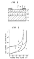
- Figure 3 is a graph which illustrates the relationships between the reverse bias voltage ar.d the dark current in order to clarify the effect of the present invention more.
- Curve A is a characteristic curve showing an example of the present invention. This example has.-a protective layer 15 of a quaternary compound semiconductor, and it has a p-n junction and a layer 13 having a spacing (l) of 1.5 ⁇ m therebetween and fulfills the foregoing condition that an electric field extending from the p-n junction does not exceed the maximum electric field of the first semiconductor layer.
- Curve B corresponds to an example which has a spacing (1) of 0.5 ⁇ m and does not satisfy the condition concerning the maximum electric field of the first semiconductor layer, and which has the protective layer 15 of the quaternary compound semiconductor.
- the reverse bias breakdown voltage is lower than in the example of the curve A, but the dark current at a low reverse bias voltage is low.
- this example is not optimized as an avalanche photodiode, it achieves the purpose of low dark current as a photodiode.
- curve C corresponds to a comparative example, which has a spacing (l) of 1.5 f m and which does not include the protective layer 15 of the quaternary compound semiconductor.
- curve D corresponds to a comparative example, which has a spacing (l) of 0.5 pm and which does not include the protective layer 15.
- Figure 4 is a sectional view of a device showing this example.
- the same symbols as in Figure 2 denote the same parts.
- the layer 15 is an InGaAsP layer for the surface protection.
- the points of difference from the embodiment in Figure 2 are that the metal of the area of the electrode 19 located under the diffused region 16 is removed, and that the electrode 18 is provided on the whole surface because no incident light is required on this side.
- the others are the same as in the example of Figure 2.
- the electric field intensity at which breakdown is caused by the tunnel effect becomes lower. Therefore, in a case where the spacing i between the plane of the p-n junction formed in the region of great forbidden band gap (e. g., InP) and the region of small forbidden band gap (e. g., InGaAsP) is small, the electric field of the material of small forbidden band gap reaches a field intensity sufficient to cause the tunnel effect and gives rise to the tunnel breakdown before the p-n junction formed in the region of great forbidden band gap causes the avalanche multiplication effect.
- the spacing i between the plane of the p-n junction formed in the region of great forbidden band gap e. g., InP
- the region of small forbidden band gap e. g., InGaAsP
- V T > V A is required in order to permit the avalanche multiplication effect to occur effectively, the impurity concentration needs to be lower than the aforementioned value. Accordingly, although the structure as shown in Figure 2 moderates to some extent, restrictions to the impurity concentration of the material of small forbidden band gap with some values of the spacing l and the impurity concentration of the material of great forbidden band gap, it is important for expecting the avalanche multiplication effect that the relation of V T > V A holds in the material of great forbidden band gap and that the maximum electric field E ms in the region of small forbidden band gap is lower than the electric field intensity E T at the tunnel breakdown (the electric field intensity E A at the avalanche breakdown, with some values of the impurity concentration).
- N L , l and E T have mutual relations, and as N L and N S are smaller, l needs to be increased more.
- the maximum electric field during the operation becomes low, but the impurity concentration of the region of small forbidden band gap needs to be limited.
- the electric field intensity E S of the material of small forbidden band gap on the side of the material of great forbidden band gap is given by the following equation: Assuming that the depletion layer is (l + W) and that W is 1 ⁇ m, the impurity concentration N S needs to be made smaller than the undermentioned value in order to prevent E S from exceeding E T . As stated above, the relation between E 9 and N S of the material must be considered.
- the lifetime of photo-excited carriers is much shorter than in Si. Therefore, in order to raise the photoelectric conversion efficiency, the light absorbing region needs to be depleted, and in order to render the operation fast, the depletion layer needs to be expanded for diminishing the junction capacitance C.
- the junction ca pi- tance is approximately given by the following equation: where ⁇ : dielectric constant, S: junction area. In view of the quantum efficiency demanded in practical use (250 %) and the junction capacitance ( ⁇ 2 pF), it is considered that the depletion layer W spreads by approximately 1 pm.
- the material system is not restricted thereto.
- a similar photo-detective semiconductor device can be realized even when, for example, a material system is used which contains GaSb principally and which employs GaAlSb as the layer 14, GaSb as the layer 13, GaSb as the layer 12 and GaAlAsSb as the layer 15.
Landscapes
- Light Receiving Elements (AREA)
Applications Claiming Priority (4)
| Application Number | Priority Date | Filing Date | Title |
|---|---|---|---|
| JP156283/81 | 1981-10-02 | ||
| JP156282/81 | 1981-10-02 | ||
| JP56156282A JPS5857760A (ja) | 1981-10-02 | 1981-10-02 | 光半導体装置 |
| JP56156283A JPS5857761A (ja) | 1981-10-02 | 1981-10-02 | 光半導体装置 |
Publications (3)
| Publication Number | Publication Date |
|---|---|
| EP0076495A2 true EP0076495A2 (de) | 1983-04-13 |
| EP0076495A3 EP0076495A3 (en) | 1984-12-05 |
| EP0076495B1 EP0076495B1 (de) | 1987-09-16 |
Family
ID=26484086
Family Applications (1)
| Application Number | Title | Priority Date | Filing Date |
|---|---|---|---|
| EP82109103A Expired EP0076495B1 (de) | 1981-10-02 | 1982-10-01 | Fotodiode |
Country Status (4)
| Country | Link |
|---|---|
| US (1) | US4740819A (de) |
| EP (1) | EP0076495B1 (de) |
| KR (1) | KR900000074B1 (de) |
| DE (1) | DE3277353D1 (de) |
Cited By (3)
| Publication number | Priority date | Publication date | Assignee | Title |
|---|---|---|---|---|
| EP0325532A3 (en) * | 1988-01-18 | 1990-05-23 | Fujitsu Limited | A semiconductor photo-diode |
| KR100746540B1 (ko) * | 2000-03-17 | 2007-08-06 | 소니 가부시끼 가이샤 | 정보 재생 장치, 정보 처리 장치, 화상 표시 제어 방법, 데이터 표시 제어 방법 및 기록 매체 |
| CN111312848A (zh) * | 2020-02-26 | 2020-06-19 | 光丰科技(浙江)有限公司 | 光电探测器、集成光电探测器及其制作方法 |
Families Citing this family (9)
| Publication number | Priority date | Publication date | Assignee | Title |
|---|---|---|---|---|
| JPS63224252A (ja) * | 1987-02-06 | 1988-09-19 | シーメンス、アクチエンゲゼルシヤフト | 導波路−ホトダイオードアレー |
| US5053837A (en) * | 1987-09-16 | 1991-10-01 | Sumitomo Electric Industries, Ltd. | Ingaas/inp type pin photodiodes |
| JPH0327577A (ja) * | 1989-06-23 | 1991-02-05 | イーストマン・コダックジャパン株式会社 | 発光ダイオ―ドアレイ |
| US5583352A (en) * | 1994-04-29 | 1996-12-10 | Eg&G Limited | Low-noise, reach-through, avalanche photodiodes |
| JP3910817B2 (ja) * | 2000-12-19 | 2007-04-25 | ユーディナデバイス株式会社 | 半導体受光装置 |
| IL156744A (en) * | 2003-07-02 | 2011-02-28 | Semi Conductor Devices An Elbit Systems Rafael Partnership | Depletion-less photodiode with suppressed dark current |
| US7049640B2 (en) * | 2004-06-30 | 2006-05-23 | The Boeing Company | Low capacitance avalanche photodiode |
| IL174844A (en) * | 2006-04-06 | 2011-02-28 | Semi Conductor Devices An Elbit Systems Rafael Partnership | Unipolar semiconductor photodetector with suppressed dark current and method for producing the same |
| EP3385989A1 (de) | 2011-09-13 | 2018-10-10 | L3 Cincinnati Electronics Corporation | Infrarotlichtdetektorvorrichtung mit vorderseitig beleuchteter barriere sowie verfahren zur herstellung davon |
Family Cites Families (13)
| Publication number | Priority date | Publication date | Assignee | Title |
|---|---|---|---|---|
| US3993506A (en) * | 1975-09-25 | 1976-11-23 | Varian Associates | Photovoltaic cell employing lattice matched quaternary passivating layer |
| FR2376513A1 (fr) * | 1976-12-31 | 1978-07-28 | Radiotechnique Compelec | Dispositif semiconducteur muni d'un film protecteur |
| US4287485A (en) * | 1977-07-18 | 1981-09-01 | Massachusetts Institute Of Technology | GaInAsP/InP Double-heterostructure lasers |
| US4213138A (en) * | 1978-12-14 | 1980-07-15 | Bell Telephone Laboratories, Incorporated | Demultiplexing photodetector |
| US4263605A (en) * | 1979-01-04 | 1981-04-21 | The United States Of America As Represented By The Secretary Of The Navy | Ion-implanted, improved ohmic contacts for GaAs semiconductor devices |
| US4231050A (en) * | 1979-01-30 | 1980-10-28 | Bell Telephone Laboratories, Incorporated | Reduction of surface recombination current in GaAs devices |
| US4328508A (en) * | 1979-04-02 | 1982-05-04 | Rca Corporation | III-V Quaternary alloy photodiode |
| US4258375A (en) * | 1979-04-09 | 1981-03-24 | Massachusetts Institute Of Technology | Gax In1-x Asy P1-y /InP Avalanche photodiode and method for its fabrication |
| US4233090A (en) * | 1979-06-28 | 1980-11-11 | Rca Corporation | Method of making a laser diode |
| US4383266A (en) * | 1979-09-26 | 1983-05-10 | Kokusai Denshin Denwa Kabushiki Kaisha | Avalanche photo diode |
| JPS5763867A (en) * | 1980-10-04 | 1982-04-17 | Nippon Telegr & Teleph Corp <Ntt> | Compound semiconductor avalanche diode |
| US4383267A (en) * | 1980-10-17 | 1983-05-10 | Rca Corporation | Avalanche photodiode and method of making same |
| JPS5793585A (en) * | 1980-12-02 | 1982-06-10 | Fujitsu Ltd | Semiconductor photoreceiving element |
-
1982
- 1982-09-27 KR KR8204346A patent/KR900000074B1/ko not_active Expired
- 1982-10-01 DE DE8282109103T patent/DE3277353D1/de not_active Expired
- 1982-10-01 EP EP82109103A patent/EP0076495B1/de not_active Expired
-
1986
- 1986-06-30 US US06/880,118 patent/US4740819A/en not_active Expired - Lifetime
Cited By (4)
| Publication number | Priority date | Publication date | Assignee | Title |
|---|---|---|---|---|
| EP0325532A3 (en) * | 1988-01-18 | 1990-05-23 | Fujitsu Limited | A semiconductor photo-diode |
| US4984032A (en) * | 1988-01-18 | 1991-01-08 | Fujitsu Limited | Semiconductor photodiode |
| KR100746540B1 (ko) * | 2000-03-17 | 2007-08-06 | 소니 가부시끼 가이샤 | 정보 재생 장치, 정보 처리 장치, 화상 표시 제어 방법, 데이터 표시 제어 방법 및 기록 매체 |
| CN111312848A (zh) * | 2020-02-26 | 2020-06-19 | 光丰科技(浙江)有限公司 | 光电探测器、集成光电探测器及其制作方法 |
Also Published As
| Publication number | Publication date |
|---|---|
| KR840001783A (ko) | 1984-05-16 |
| KR900000074B1 (ko) | 1990-01-19 |
| US4740819A (en) | 1988-04-26 |
| EP0076495A3 (en) | 1984-12-05 |
| EP0076495B1 (de) | 1987-09-16 |
| DE3277353D1 (en) | 1987-10-22 |
Similar Documents
| Publication | Publication Date | Title |
|---|---|---|
| EP0163295B1 (de) | Halbleiterphotodetektor und Verfahren zu seiner Herstellung | |
| EP0675549B1 (de) | Lawinenphotodiode mit Übergitter | |
| EP0156156A1 (de) | Avalanche-Photodioden | |
| US4731641A (en) | Avalanche photo diode with quantum well layer | |
| EP1811578B1 (de) | Avalanche-fotodiode | |
| US7415185B2 (en) | Buried-waveguide-type light receiving element and manufacturing method thereof | |
| US5539221A (en) | Staircase avalanche photodiode | |
| EP0076495B1 (de) | Fotodiode | |
| JP2708409B2 (ja) | 半導体受光素子およびその製造方法 | |
| CA2050435C (en) | Photo-sensing device | |
| EP0325532B1 (de) | Halbleiterphotodiode | |
| US5432361A (en) | Low noise avalanche photodiode having an avalanche multiplication layer of InAlAs/InGaAlAs | |
| US4700209A (en) | Avalanche photodiode and a method of making same | |
| EP0108561B1 (de) | Halbleiteranordnung zum Empfangen von Licht und Abgabe eines elektrischen Signals | |
| US4587544A (en) | Avalanche photodetector | |
| CA2050363A1 (en) | Photo-sensing device | |
| EP0308335B1 (de) | InGaAs/InP-PIN-Photodioden | |
| US4561007A (en) | Double mesa avalanche photodetector | |
| US4914494A (en) | Avalanche photodiode with central zone in active and absorptive layers | |
| US4816890A (en) | Optoelectronic device | |
| JPS6244709B2 (de) | ||
| JP2633234B2 (ja) | 光半導体素子 | |
| JPH051629B2 (de) | ||
| JPS63281480A (ja) | 半導体受光素子及びその製造方法 | |
| US4918508A (en) | Vertical photoconductive detector |
Legal Events
| Date | Code | Title | Description |
|---|---|---|---|
| PUAI | Public reference made under article 153(3) epc to a published international application that has entered the european phase |
Free format text: ORIGINAL CODE: 0009012 |
|
| AK | Designated contracting states |
Designated state(s): DE FR GB IT |
|
| PUAL | Search report despatched |
Free format text: ORIGINAL CODE: 0009013 |
|
| AK | Designated contracting states |
Designated state(s): DE FR GB IT |
|
| 17P | Request for examination filed |
Effective date: 19841220 |
|
| 17Q | First examination report despatched |
Effective date: 19860213 |
|
| GRAA | (expected) grant |
Free format text: ORIGINAL CODE: 0009210 |
|
| AK | Designated contracting states |
Kind code of ref document: B1 Designated state(s): DE FR GB IT |
|
| REF | Corresponds to: |
Ref document number: 3277353 Country of ref document: DE Date of ref document: 19871022 |
|
| ITF | It: translation for a ep patent filed | ||
| ET | Fr: translation filed | ||
| PLBE | No opposition filed within time limit |
Free format text: ORIGINAL CODE: 0009261 |
|
| STAA | Information on the status of an ep patent application or granted ep patent |
Free format text: STATUS: NO OPPOSITION FILED WITHIN TIME LIMIT |
|
| 26N | No opposition filed | ||
| ITTA | It: last paid annual fee | ||
| PGFP | Annual fee paid to national office [announced via postgrant information from national office to epo] |
Ref country code: GB Payment date: 20000921 Year of fee payment: 19 |
|
| PGFP | Annual fee paid to national office [announced via postgrant information from national office to epo] |
Ref country code: FR Payment date: 20001019 Year of fee payment: 19 |
|
| PGFP | Annual fee paid to national office [announced via postgrant information from national office to epo] |
Ref country code: DE Payment date: 20001221 Year of fee payment: 19 |
|
| PG25 | Lapsed in a contracting state [announced via postgrant information from national office to epo] |
Ref country code: GB Free format text: LAPSE BECAUSE OF NON-PAYMENT OF DUE FEES Effective date: 20011001 |
|
| REG | Reference to a national code |
Ref country code: GB Ref legal event code: IF02 |
|
| GBPC | Gb: european patent ceased through non-payment of renewal fee |
Effective date: 20011001 |
|
| PG25 | Lapsed in a contracting state [announced via postgrant information from national office to epo] |
Ref country code: FR Free format text: LAPSE BECAUSE OF NON-PAYMENT OF DUE FEES Effective date: 20020628 |
|
| PG25 | Lapsed in a contracting state [announced via postgrant information from national office to epo] |
Ref country code: DE Free format text: LAPSE BECAUSE OF NON-PAYMENT OF DUE FEES Effective date: 20020702 |
|
| REG | Reference to a national code |
Ref country code: FR Ref legal event code: ST |