EP0076587A2 - Verfahren zur Herstellung von Dünnschichttransistoren - Google Patents
Verfahren zur Herstellung von Dünnschichttransistoren Download PDFInfo
- Publication number
- EP0076587A2 EP0076587A2 EP82304917A EP82304917A EP0076587A2 EP 0076587 A2 EP0076587 A2 EP 0076587A2 EP 82304917 A EP82304917 A EP 82304917A EP 82304917 A EP82304917 A EP 82304917A EP 0076587 A2 EP0076587 A2 EP 0076587A2
- Authority
- EP
- European Patent Office
- Prior art keywords
- layer
- insulator
- portions
- substrate
- semiconductor
- Prior art date
- Legal status (The legal status is an assumption and is not a legal conclusion. Google has not performed a legal analysis and makes no representation as to the accuracy of the status listed.)
- Granted
Links
Images

Classifications
-
- H—ELECTRICITY
- H10—SEMICONDUCTOR DEVICES; ELECTRIC SOLID-STATE DEVICES NOT OTHERWISE PROVIDED FOR
- H10D—INORGANIC ELECTRIC SEMICONDUCTOR DEVICES
- H10D86/00—Integrated devices formed in or on insulating or conducting substrates, e.g. formed in silicon-on-insulator [SOI] substrates or on stainless steel or glass substrates
- H10D86/01—Manufacture or treatment
- H10D86/021—Manufacture or treatment of multiple TFTs
- H10D86/0231—Manufacture or treatment of multiple TFTs using masks, e.g. half-tone masks
-
- H—ELECTRICITY
- H10—SEMICONDUCTOR DEVICES; ELECTRIC SOLID-STATE DEVICES NOT OTHERWISE PROVIDED FOR
- H10D—INORGANIC ELECTRIC SEMICONDUCTOR DEVICES
- H10D30/00—Field-effect transistors [FET]
- H10D30/60—Insulated-gate field-effect transistors [IGFET]
- H10D30/67—Thin-film transistors [TFT]
- H10D30/674—Thin-film transistors [TFT] characterised by the active materials
- H10D30/675—Group III-V materials, Group II-VI materials, Group IV-VI materials, selenium or tellurium
-
- H—ELECTRICITY
- H10—SEMICONDUCTOR DEVICES; ELECTRIC SOLID-STATE DEVICES NOT OTHERWISE PROVIDED FOR
- H10D—INORGANIC ELECTRIC SEMICONDUCTOR DEVICES
- H10D64/00—Electrodes of devices having potential barriers
- H10D64/01—Manufacture or treatment
- H10D64/011—Manufacture or treatment of electrodes ohmically coupled to a semiconductor
-
- H—ELECTRICITY
- H10—SEMICONDUCTOR DEVICES; ELECTRIC SOLID-STATE DEVICES NOT OTHERWISE PROVIDED FOR
- H10D—INORGANIC ELECTRIC SEMICONDUCTOR DEVICES
- H10D86/00—Integrated devices formed in or on insulating or conducting substrates, e.g. formed in silicon-on-insulator [SOI] substrates or on stainless steel or glass substrates
- H10D86/40—Integrated devices formed in or on insulating or conducting substrates, e.g. formed in silicon-on-insulator [SOI] substrates or on stainless steel or glass substrates characterised by multiple TFTs
- H10D86/60—Integrated devices formed in or on insulating or conducting substrates, e.g. formed in silicon-on-insulator [SOI] substrates or on stainless steel or glass substrates characterised by multiple TFTs wherein the TFTs are in active matrices
-
- Y—GENERAL TAGGING OF NEW TECHNOLOGICAL DEVELOPMENTS; GENERAL TAGGING OF CROSS-SECTIONAL TECHNOLOGIES SPANNING OVER SEVERAL SECTIONS OF THE IPC; TECHNICAL SUBJECTS COVERED BY FORMER USPC CROSS-REFERENCE ART COLLECTIONS [XRACs] AND DIGESTS
- Y10—TECHNICAL SUBJECTS COVERED BY FORMER USPC
- Y10S—TECHNICAL SUBJECTS COVERED BY FORMER USPC CROSS-REFERENCE ART COLLECTIONS [XRACs] AND DIGESTS
- Y10S148/00—Metal treatment
- Y10S148/063—Gp II-IV-VI compounds
-
- Y—GENERAL TAGGING OF NEW TECHNOLOGICAL DEVELOPMENTS; GENERAL TAGGING OF CROSS-SECTIONAL TECHNOLOGIES SPANNING OVER SEVERAL SECTIONS OF THE IPC; TECHNICAL SUBJECTS COVERED BY FORMER USPC CROSS-REFERENCE ART COLLECTIONS [XRACs] AND DIGESTS
- Y10—TECHNICAL SUBJECTS COVERED BY FORMER USPC
- Y10S—TECHNICAL SUBJECTS COVERED BY FORMER USPC CROSS-REFERENCE ART COLLECTIONS [XRACs] AND DIGESTS
- Y10S148/00—Metal treatment
- Y10S148/10—Lift-off masking
-
- Y—GENERAL TAGGING OF NEW TECHNOLOGICAL DEVELOPMENTS; GENERAL TAGGING OF CROSS-SECTIONAL TECHNOLOGIES SPANNING OVER SEVERAL SECTIONS OF THE IPC; TECHNICAL SUBJECTS COVERED BY FORMER USPC CROSS-REFERENCE ART COLLECTIONS [XRACs] AND DIGESTS
- Y10—TECHNICAL SUBJECTS COVERED BY FORMER USPC
- Y10S—TECHNICAL SUBJECTS COVERED BY FORMER USPC CROSS-REFERENCE ART COLLECTIONS [XRACs] AND DIGESTS
- Y10S148/00—Metal treatment
- Y10S148/105—Masks, metal
-
- Y—GENERAL TAGGING OF NEW TECHNOLOGICAL DEVELOPMENTS; GENERAL TAGGING OF CROSS-SECTIONAL TECHNOLOGIES SPANNING OVER SEVERAL SECTIONS OF THE IPC; TECHNICAL SUBJECTS COVERED BY FORMER USPC CROSS-REFERENCE ART COLLECTIONS [XRACs] AND DIGESTS
- Y10—TECHNICAL SUBJECTS COVERED BY FORMER USPC
- Y10S—TECHNICAL SUBJECTS COVERED BY FORMER USPC CROSS-REFERENCE ART COLLECTIONS [XRACs] AND DIGESTS
- Y10S148/00—Metal treatment
- Y10S148/169—Vacuum deposition, e.g. including molecular beam epitaxy
-
- Y—GENERAL TAGGING OF NEW TECHNOLOGICAL DEVELOPMENTS; GENERAL TAGGING OF CROSS-SECTIONAL TECHNOLOGIES SPANNING OVER SEVERAL SECTIONS OF THE IPC; TECHNICAL SUBJECTS COVERED BY FORMER USPC CROSS-REFERENCE ART COLLECTIONS [XRACs] AND DIGESTS
- Y10—TECHNICAL SUBJECTS COVERED BY FORMER USPC
- Y10S—TECHNICAL SUBJECTS COVERED BY FORMER USPC CROSS-REFERENCE ART COLLECTIONS [XRACs] AND DIGESTS
- Y10S438/00—Semiconductor device manufacturing: process
- Y10S438/913—Diverse treatments performed in unitary chamber
-
- Y—GENERAL TAGGING OF NEW TECHNOLOGICAL DEVELOPMENTS; GENERAL TAGGING OF CROSS-SECTIONAL TECHNOLOGIES SPANNING OVER SEVERAL SECTIONS OF THE IPC; TECHNICAL SUBJECTS COVERED BY FORMER USPC CROSS-REFERENCE ART COLLECTIONS [XRACs] AND DIGESTS
- Y10—TECHNICAL SUBJECTS COVERED BY FORMER USPC
- Y10S—TECHNICAL SUBJECTS COVERED BY FORMER USPC CROSS-REFERENCE ART COLLECTIONS [XRACs] AND DIGESTS
- Y10S438/00—Semiconductor device manufacturing: process
- Y10S438/98—Utilizing process equivalents or options
Definitions
- This invention broadly relates to a process for forming a device by selective deposition and patterning of thin film layers of insulative, semiconductive, and conductive materials. More particularly, the invention concerns an improved method of forming such a device wherein thin film layers of insulator, semiconductor, and metal are deposited in successive sequence under continuous vacuum.
- the invention has particular utility in the photolithographic fabrication of thin film transistors and arrays thereof. In the fabrication of such devices, single pump down formation of the semiconductor-gate insulator and semiconductor-source/drain contact interfaces minimizes the exposure of these critical interfaces to contamination during wet processing.
- wet chemistry processes to selectively define patterned layers of conductive and insulative materials. These wet processes include chemical polish etching for initial substrate preparation, structural, or patten delineation, etching to create a relief structure geometry, and photoresist processing.
- the electrical performance and the stability of surface field effect transistors are critically dependent upon the quality of the semiconductor-insulator interface and upon the ohmic properties of source drain contacts to semiconductor interface.
- the quality of both interfaces can be impaired by impurity contamination arising from exposure of each material (i.e. conductor, insulator, and semiconductor) surface to wet processing. Such contamination increases the densities of interface states and reduces conduction modulation.
- Incorporation of ionic species present in the chemical solution alters the otherwise predictable threshold voltages. Charge transfer processes at interface states and field aided migration of mobile ionic species induces operational instabilities into the devices. Impurity related contact barriers degrade transconductance by limiting current and crowding transistor characteristics.
- the present invention provides a process for overcoming the disadvantages which can arise from exposure of critical surfaces of the constituent layers of the thin film device to wet processing.
- the present invention provides methods for preserving the integrity of the interfaces between layers of semiconductor and insulator and semiconductor and conductor during formation of a thin film device. This is achieved by depositing the layers of insulator, semiconductor, and conductor in the desired sequence under continuous vacuum, i.e. in a single vacuum pump down operation. This technique effectively seals, or encapsulates, the damage (i.e. contamination or impurity) sensitive semiconductor so that subsequent wet processing steps do not adversely affect the electrical characteristics of the device by contaminating critical interfaces. In addition, sequential deposition of these layers under vacuum affords protection of the semiconductor interfaces against degradation by airborne contaminants.
- the invention minimizes contamination exposure of the critical interfaces between the semiconductor and gate and semiconductor and source and drain contacts of a thin film transistor.
- exemplary of this method is a fabrication sequence utilizing aluminum, silicon dioxide, cadmium selenide, and chromium and aluminum, for the gate electrode, gate insulator, semiconductor, and source and drain contacts, respectively.
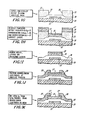
- the initial step in this sequence is the formation of the aluminum gate electrode on a portion of a surface of a substrate by, for example, additive photolithographic delineation.
- An additive photoresist mask is then formed for definition of the semiconductor pad.
- the silicon dioxide gate insulator, cadmium selenide, and chromium contact layers are then sequentially deposited through the apertures in the additive mask during a single vacuum pump down to form the critical semiconductor-insulator interface and semiconductor-source and drain contacts.
- the chromium contact layer functions as a protective cap over the semiconductor pad, preventing harmful interaction between the semiconductor and the stripping solution, Le. the solvent per se or ionic species contained therein.
- Two steps remain for completion of the thin film transistor, i.e. removal of that portion of the chromium layer overlying the conducting channel of the semiconductor, and definition of the aluminum source and drain network.
- the aluminum source and drain electrodes are formed by additive processing to provide a structure wherein respective source and drain electrodes are separated by a gap corresponding to the width of the conducting channel of the semiconductor layer and exposing portions of the chromium layer.
- the aluminum source drain network structure functions as a subtractive mask through which chromium is selectively removed from the thin film transistor conducting channel by dry etching techniques.
- dry etching techniques e.g. plasma etching
- cleaning techniques are preferred for this final step because of the high degee of etch selectivity and "cleanliness" which are characteristic of such processes.
- the sequence for fabricating a thin film transistor includes the step of depositing an initial layer of insulative material to cover the gate electrode and the entire surface of the substrate on which the gate electrode is formed. Utilization of this process to provide a "full" rather than patterned insulator layer over the substrate and gate electrode is particularly advantageous as a means for enhancing the insulation between source and gate electrode gate crossovers in a multitransistor array.
- the side wall surfaces of the openings in the photoresist mask used to define the semiconductor pad are coated with a thin film of insulator, e.g. silicon dioxide, prior to the single pump down sequential deposition of the critical device layers. This step ensures minimum contamination of the electronically active regions of the device by complete isolation thereof from organic materials present during removal of the photoresist mask.
- insulator e.g. silicon dioxide
- resist 14 can comprise conventional photo or electron beam materials which are characterized by radiation-induced alteration in solubility that enables subsequent removal with aqueous solutions.
- a suitable material is Shipley's AZ 1350B or AZ 1350J sold by Shipley Company, Inc., of Newton, MA.
- Resist 14 is applied in any conventional manner, as for example, by spin coating. Thereafter, in accordance with well known photolithographic techniques, resist layer 14 is processed into an additive mask by conventional steps of exposure, development, and removal of selective pattern areas thereof.
- a 100 nm layer of aluminum is deposited, as by vacuum evaporation, sputtering, or the like, over the surface of the mask substrate.
- This aluminum layer 16 is deposited through the apertures in the photoresist mask onto the surface of the substrate 10 to form gate electrode 12 and on top of the remaining portions of resist layer 14.
- the remaining portions of resist 14 and the overlying aluminum layer 16 are removed using conventional removal techniques, e.g. by exposing the structure to a solvent suited to the solubility of the resist 14.
- a blanket layer 18 of aluminum oxide or silicon dioxide is deposited over the gate electrode 12 and the exposed surface of substrate 10.
- This insulative layer can be applied in any conventional manner, as for example, by evaporation or sputtering within a suitable vacuum device.
- coverage of the complete active surface of the substrate is desirable for multi transistor arrays. From a practical standpoint, complete coverage of the entire surface of the substrate is not preferred, since the contact fingers for the away bus lines are typically located around the periphery of the substrate.
- a second blanket layer of resist 11 is applied over insulator 18 as illustrated in Figure IF.
- various solvent soluble materials may be chosen for the resist layer 11, the same being applied by any of the well known techniques such as spinning, spraying, dipping or the like.
- resist layer 11 is exposed and developed in a pattern corresponding to the desired dimensions of the semiconductor pad for the thin film transistor as illustrated by the structure of Figure 1 G.
- the patterned resist layer 11 is used as an additive mask for depositing, in sequence, layers of insulator (Si0 2 ) 13, semiconductor (CdSe) 15, and conductor (Cr) 17. It is of critical importance to the invention that these layers be deposited under the continuous vacuum of a single pump down operation. This is accomplished by placing the structure of Figure 1 G into any suitable vacuum chamber and reducing the pressure to about 0.66 ⁇ Nm -2 . Thereafter, utilizing conventional deposition techniques of the integrated circuit fabrication art, the layers of Si0 2 , CdSe, and Cr are deposited in succession. The pressure for deposition of Si0 2 could consist of 66 ⁇ Nm -2 partial pressure of oxygen.
- the initial deposition of a thin additional layer of insulator 13 onto the pre- existing insulator layer 18 provides a clean insulative interface for the subsequently deposited semiconductor layer 15, isolating the same from any contaminants or impurities introduced onto the surface of insulator 18 during the process of forming the additive mask thereon or during handling of the substrate or exposure thereof to air.
- a thickness of about 80 nm for insulator layer 13 has been found to be adequate for these purposes.
- a layer of CdSe is deposited to a thickness of about 30 nm followed by deposition of a layer of Cr to a thickness of about 50 nm.
- the layer of resist 11 and all of the layers overlying it are removed by exposing the coated substrate of Figure 1H to a suitable solvent for resist 11.
- suitable solvents include acetone and other commercially available strippers.
- maximum immunity against contamination of the electronically active device regions is achieved by lining the side walls 19 of the apertures in resist layer 11 with a thin film of insulator (Si0 2 ) prior to deposition of layers 15 and 17. This additional step (which is not shown) completely isolates the critical regions of the device from the organic materials utilized in the subsequent processing.
- a protective layer of silicon dioxide can be deposited as a separate step or concurrently with the deposition of layer 13.
- the structure is as shown in Figure lI.
- the chromium film acts as a protective cap to isolate the upper surface of semiconductor pad 15 from processing contaminants in the solvent.
- the completed thin film transistor structure is shown having source and drain electrodes 20 electrically connected to the semiconductor through chromium contacts 17'.
- source and drain electrodes 20 are formed by conventional additive processing to yield the structure of Figure 1J.
- the source and drain electrodes 20 are aluminum and are patterned so as to expose the chromium contact layer 17.
- the source and drain electrode network is employed as a subtractive mask during selective dry etching of chromium from the conducting channel of the thin film transistor. Dry etching techniques are preferred for this step because of the characteristic cleanliness of such methods as well as the high degree of directionality offered thereby.
- Plasma etching utilizing a reaction gas, e.g. CC1 4 vapor in air or oxygen has been found to be particularly effective in removing chromium in the embodiment illustrated herein.
- the conductive material chosen for the source and drain contacts 20 must be resistant to the plasma employed to etch the conductive contact layer 17. While other materials may be used, aluminum deposited to a desired thickness of about 100 nm has been demonstrated to be sufficiently resistant to plasma etching in a reaction gas, such as mentioned above. It will be appreciated that selection of other materials for the source and drain electrodes 20 and the contacts 17' and the choice of a suitable ambient atmosphere for the selected materials other than those described herein are possible.
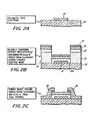
- Figures 2A - 2C An alternative sequence for fabricating a thin film transistor is illustrated in Figures 2A - 2C.
- Figure 2A illustrates a gate electrode 32 formed upon a substrate 30.
- This structure corresponds to the structure illustrated in Figure 1D and is produced by any suitable deposition techniques, such as the additive process discussed in conjunction with Figures lA - 1D.
- an additive mask is formed by exposure and development of a resist layer 31 which is applied to the structure of Figure 2A. Unlike the process discussed with reference to Figures lA - 1K, there is no initial deposition of an insulator layer such as layer 18 of Figure lE. Instead, the resist is coated directly over the exposed surfaces of substrate 30 and gate electrode 32. Thereafter, using standard lithographic techniques, portions of the resist layer are selectively removed to expose the gate electrode 32 and portions of the surface of substrate 30 adjacent the gate electrode to form an additive mask.
- insulator (Si0 2 ) semiconductor (CdSe), and conductor (Cr) are deposited onto the mask structure during a single vacuum pump down operation by means such as discussed in conjunction with Figure 1H.
- the resulting structure is illustrated in Figure 2B, wherein it will be noted that, by virtue of the selected pattern in the resist mask, that portion of the deposited insulator designated 33A forms a gate insulator layer which covers both upper and side surfaces of gate electrode 32.
Landscapes
- Thin Film Transistor (AREA)
- Weting (AREA)
- Drying Of Semiconductors (AREA)
Applications Claiming Priority (2)
| Application Number | Priority Date | Filing Date | Title |
|---|---|---|---|
| US06/307,463 US4404731A (en) | 1981-10-01 | 1981-10-01 | Method of forming a thin film transistor |
| US307463 | 1981-10-01 |
Publications (3)
| Publication Number | Publication Date |
|---|---|
| EP0076587A2 true EP0076587A2 (de) | 1983-04-13 |
| EP0076587A3 EP0076587A3 (en) | 1984-03-28 |
| EP0076587B1 EP0076587B1 (de) | 1986-12-10 |
Family
ID=23189890
Family Applications (1)
| Application Number | Title | Priority Date | Filing Date |
|---|---|---|---|
| EP82304917A Expired EP0076587B1 (de) | 1981-10-01 | 1982-09-17 | Verfahren zur Herstellung von Dünnschichttransistoren |
Country Status (5)
| Country | Link |
|---|---|
| US (1) | US4404731A (de) |
| EP (1) | EP0076587B1 (de) |
| JP (1) | JPS5871665A (de) |
| CA (1) | CA1186420A (de) |
| DE (1) | DE3274700D1 (de) |
Cited By (6)
| Publication number | Priority date | Publication date | Assignee | Title |
|---|---|---|---|---|
| FR2553579A1 (fr) * | 1983-10-12 | 1985-04-19 | Commissariat Energie Atomique | Procede de fabrication d'un transistor en film mince a grille auto-alignee |
| FR2566583A1 (fr) * | 1984-06-22 | 1985-12-27 | Thomson Csf | Procede de fabrication d'au moins un transistor a effet de champ en couche mince, et transistor obtenu par ce procede |
| EP0102802B1 (de) * | 1982-08-23 | 1987-03-11 | Xerox Corporation | Photolithographisches Verfahren zur Herstellung von Dünnfilmtransistoren |
| EP0222668A1 (de) * | 1985-11-15 | 1987-05-20 | Commissariat A L'energie Atomique | Verfahren zum Herstellen eines Dünnschichttransistors mit in Bezug auf Source und Drain selbstausrichtendem Gate durch stufenweises Ätzen und danach hergestellter Transistor |
| EP0493113A3 (en) * | 1990-12-28 | 1992-09-02 | Sharp Kabushiki Kaisha | A method for producing an active matrix substrate for liquid crystal display devices |
| US5474941A (en) * | 1990-12-28 | 1995-12-12 | Sharp Kabushiki Kaisha | Method for producing an active matrix substrate |
Families Citing this family (10)
| Publication number | Priority date | Publication date | Assignee | Title |
|---|---|---|---|---|
| US6786997B1 (en) | 1984-11-26 | 2004-09-07 | Semiconductor Energy Laboratory Co., Ltd. | Plasma processing apparatus |
| JPH0752718B2 (ja) | 1984-11-26 | 1995-06-05 | 株式会社半導体エネルギー研究所 | 薄膜形成方法 |
| DE3604368A1 (de) * | 1985-02-13 | 1986-08-14 | Sharp K.K., Osaka | Verfahren zur herstellung eines duennfilm-transistors |
| GB9902252D0 (en) * | 1999-02-03 | 1999-03-24 | Philips Electronics Nv | X-ray filter and x-ray examination apparatus using the same |
| GB0013473D0 (en) * | 2000-06-03 | 2000-07-26 | Univ Liverpool | A method of electronic component fabrication and an electronic component |
| JP4841751B2 (ja) * | 2001-06-01 | 2011-12-21 | 株式会社半導体エネルギー研究所 | 有機半導体装置及びその作製方法 |
| TW200421439A (en) * | 2003-04-04 | 2004-10-16 | Innolux Display Corp | Photo-mask process and the method of fabricating a thin film transistor |
| US20070178710A1 (en) * | 2003-08-18 | 2007-08-02 | 3M Innovative Properties Company | Method for sealing thin film transistors |
| TW201006021A (en) * | 2008-07-31 | 2010-02-01 | Nat Univ Tsing Hua | An organic field effect transistor and its manufacturing method |
| US9985137B2 (en) * | 2013-12-16 | 2018-05-29 | Japan Advanced Institute Of Science And Technology | Semiconductor device having a decomposed aliphatic polycarbonate layer |
Family Cites Families (13)
| Publication number | Priority date | Publication date | Assignee | Title |
|---|---|---|---|---|
| NL294370A (de) * | 1963-06-20 | |||
| NL6604962A (de) * | 1966-04-14 | 1967-10-16 | ||
| US3627662A (en) * | 1970-02-24 | 1971-12-14 | Gte Laboratories Inc | Thin film transistor and method of fabrication thereof |
| US3669661A (en) * | 1970-03-06 | 1972-06-13 | Westinghouse Electric Corp | Method of producing thin film transistors |
| US3914127A (en) * | 1973-11-23 | 1975-10-21 | Texas Instruments Inc | Method of making charge-coupled devices |
| US4065781A (en) * | 1974-06-21 | 1977-12-27 | Westinghouse Electric Corporation | Insulated-gate thin film transistor with low leakage current |
| US3985597A (en) * | 1975-05-01 | 1976-10-12 | International Business Machines Corporation | Process for forming passivated metal interconnection system with a planar surface |
| US4040073A (en) * | 1975-08-29 | 1977-08-02 | Westinghouse Electric Corporation | Thin film transistor and display panel using the transistor |
| US4132586A (en) * | 1977-12-20 | 1979-01-02 | International Business Machines Corporation | Selective dry etching of substrates |
| JPS5499576A (en) * | 1978-01-23 | 1979-08-06 | Sharp Corp | Thin-film transistor and its manufacture |
| US4145459A (en) * | 1978-02-02 | 1979-03-20 | Rca Corporation | Method of making a short gate field effect transistor |
| JPS54154289A (en) * | 1978-05-26 | 1979-12-05 | Matsushita Electric Ind Co Ltd | Manufacture of thin-film transistor array |
| US4343081A (en) * | 1979-06-22 | 1982-08-10 | L'etat Francais Represente Par Le Secretaire D'etat Aux Postes Et Telecommunications Et A La Telediffusion (Centre National D'etudes Des Telecommunications) | Process for making semi-conductor devices |
-
1981
- 1981-10-01 US US06/307,463 patent/US4404731A/en not_active Expired - Lifetime
-
1982
- 1982-09-15 CA CA000411416A patent/CA1186420A/en not_active Expired
- 1982-09-17 DE DE8282304917T patent/DE3274700D1/de not_active Expired
- 1982-09-17 EP EP82304917A patent/EP0076587B1/de not_active Expired
- 1982-09-22 JP JP57165972A patent/JPS5871665A/ja active Pending
Cited By (13)
| Publication number | Priority date | Publication date | Assignee | Title |
|---|---|---|---|---|
| EP0102802B1 (de) * | 1982-08-23 | 1987-03-11 | Xerox Corporation | Photolithographisches Verfahren zur Herstellung von Dünnfilmtransistoren |
| EP0139585A1 (de) * | 1983-10-12 | 1985-05-02 | Commissariat A L'energie Atomique | Verfahren zum Herstellen eines Dünnfilmtransistors mit selbstausrichtendem Gate |
| US4587720A (en) * | 1983-10-12 | 1986-05-13 | Commissariat A L'energie Atomique | Process for the manufacture of a self-aligned thin-film transistor |
| FR2553579A1 (fr) * | 1983-10-12 | 1985-04-19 | Commissariat Energie Atomique | Procede de fabrication d'un transistor en film mince a grille auto-alignee |
| US4704784A (en) * | 1984-06-22 | 1987-11-10 | Thomson-Csf | Method of making thin film field effect transistors for a liquid crystal display device |
| FR2566583A1 (fr) * | 1984-06-22 | 1985-12-27 | Thomson Csf | Procede de fabrication d'au moins un transistor a effet de champ en couche mince, et transistor obtenu par ce procede |
| EP0165863A1 (de) * | 1984-06-22 | 1985-12-27 | Thomson-Csf | Verfahren zum Herstellen von mindestens einem Dünnfilm-Feldeffekttransistor und nach diesem Verfahren hergestellter Transistor |
| EP0222668A1 (de) * | 1985-11-15 | 1987-05-20 | Commissariat A L'energie Atomique | Verfahren zum Herstellen eines Dünnschichttransistors mit in Bezug auf Source und Drain selbstausrichtendem Gate durch stufenweises Ätzen und danach hergestellter Transistor |
| FR2590409A1 (fr) * | 1985-11-15 | 1987-05-22 | Commissariat Energie Atomique | Procede de fabrication d'un transistor en couches minces a grille auto-alignee par rapport au drain et a la source de celui-ci et transistor obtenu par le procede |
| US4715930A (en) * | 1985-11-15 | 1987-12-29 | Commissariat A L'energie Atomique | Process for producing by sloping etching a thin film transistor with a self-aligned gate with respect to the drain and source thereof |
| EP0493113A3 (en) * | 1990-12-28 | 1992-09-02 | Sharp Kabushiki Kaisha | A method for producing an active matrix substrate for liquid crystal display devices |
| US5286659A (en) * | 1990-12-28 | 1994-02-15 | Sharp Kabushiki Kaisha | Method for producing an active matrix substrate |
| US5474941A (en) * | 1990-12-28 | 1995-12-12 | Sharp Kabushiki Kaisha | Method for producing an active matrix substrate |
Also Published As
| Publication number | Publication date |
|---|---|
| US4404731A (en) | 1983-09-20 |
| EP0076587B1 (de) | 1986-12-10 |
| EP0076587A3 (en) | 1984-03-28 |
| CA1186420A (en) | 1985-04-30 |
| DE3274700D1 (en) | 1987-01-22 |
| JPS5871665A (ja) | 1983-04-28 |
Similar Documents
| Publication | Publication Date | Title |
|---|---|---|
| EP0076587B1 (de) | Verfahren zur Herstellung von Dünnschichttransistoren | |
| EP0643420B1 (de) | Lift-off Verfahren für selbstausrichtende Dünnschichttransistoren | |
| CA1202121A (en) | Photolithographic process for fabricating thin film transistors | |
| US4704783A (en) | Method for passivating the back channel of amorphous silicon field effect transistors | |
| KR980006510A (ko) | 반도체 장치의 제조방법 | |
| EP0646953B1 (de) | Methode zur Reduzierung des Leckstroms in Dünnfilmtransistoren | |
| EP0020929A1 (de) | Feldeffekttransistoren | |
| US4222816A (en) | Method for reducing parasitic capacitance in integrated circuit structures | |
| EP0656645A2 (de) | Feldeffekttransistor mit einem diffusionierten versiegelten Übergang | |
| KR970006733B1 (ko) | 박막트랜지스터 제조방법 | |
| US4751554A (en) | Silicon-on-sapphire integrated circuit and method of making the same | |
| KR100253394B1 (ko) | 듀얼 게이트절연막을 가지는 게이트전극의 제조방법 | |
| EP0544069B1 (de) | Dünnschicht-Transistor-Panel und dessen Herstellungsmethode | |
| JPS61224360A (ja) | 電界効果トランジスタの製造方法 | |
| US6127272A (en) | Method of electron beam lithography on very high resistivity substrates | |
| JP2913737B2 (ja) | 薄膜トランジスタの製造方法 | |
| US5627103A (en) | Method of thin film transistor formation with split polysilicon deposition | |
| CN112335048A (zh) | 晶体管阵列 | |
| KR100218730B1 (ko) | 반도체 소자 제조방법 | |
| JPH06252402A (ja) | 薄膜トランジスタの製造方法 | |
| JPH05291295A (ja) | 薄膜トランジスタの製造方法 | |
| KR0166030B1 (ko) | 반도체 소자의 캐패시터 제조방법 | |
| KR100328824B1 (ko) | 커패시터 제조방법 | |
| KR910001193B1 (ko) | 반도체 장치의 제조방법 | |
| JPH06151459A (ja) | 薄膜トランジスタの製造方法 |
Legal Events
| Date | Code | Title | Description |
|---|---|---|---|
| PUAI | Public reference made under article 153(3) epc to a published international application that has entered the european phase |
Free format text: ORIGINAL CODE: 0009012 |
|
| AK | Designated contracting states |
Designated state(s): DE GB NL |
|
| PUAL | Search report despatched |
Free format text: ORIGINAL CODE: 0009013 |
|
| AK | Designated contracting states |
Designated state(s): DE GB NL |
|
| 17P | Request for examination filed |
Effective date: 19840710 |
|
| GRAA | (expected) grant |
Free format text: ORIGINAL CODE: 0009210 |
|
| AK | Designated contracting states |
Kind code of ref document: B1 Designated state(s): DE GB NL |
|
| REF | Corresponds to: |
Ref document number: 3274700 Country of ref document: DE Date of ref document: 19870122 |
|
| PLBE | No opposition filed within time limit |
Free format text: ORIGINAL CODE: 0009261 |
|
| STAA | Information on the status of an ep patent application or granted ep patent |
Free format text: STATUS: NO OPPOSITION FILED WITHIN TIME LIMIT |
|
| 26N | No opposition filed | ||
| PGFP | Annual fee paid to national office [announced via postgrant information from national office to epo] |
Ref country code: GB Payment date: 19990915 Year of fee payment: 18 |
|
| PGFP | Annual fee paid to national office [announced via postgrant information from national office to epo] |
Ref country code: DE Payment date: 19990927 Year of fee payment: 18 |
|
| PGFP | Annual fee paid to national office [announced via postgrant information from national office to epo] |
Ref country code: NL Payment date: 19990930 Year of fee payment: 18 |
|
| PG25 | Lapsed in a contracting state [announced via postgrant information from national office to epo] |
Ref country code: GB Free format text: LAPSE BECAUSE OF NON-PAYMENT OF DUE FEES Effective date: 20000917 |
|
| PG25 | Lapsed in a contracting state [announced via postgrant information from national office to epo] |
Ref country code: NL Free format text: LAPSE BECAUSE OF NON-PAYMENT OF DUE FEES Effective date: 20010401 |
|
| GBPC | Gb: european patent ceased through non-payment of renewal fee |
Effective date: 20000917 |
|
| NLV4 | Nl: lapsed or anulled due to non-payment of the annual fee |
Effective date: 20010401 |
|
| PG25 | Lapsed in a contracting state [announced via postgrant information from national office to epo] |
Ref country code: DE Free format text: LAPSE BECAUSE OF NON-PAYMENT OF DUE FEES Effective date: 20010601 |