EP0077207A1 - Procédé et appareil activé par laser pour dépôt chimique - Google Patents
Procédé et appareil activé par laser pour dépôt chimique Download PDFInfo
- Publication number
- EP0077207A1 EP0077207A1 EP82305407A EP82305407A EP0077207A1 EP 0077207 A1 EP0077207 A1 EP 0077207A1 EP 82305407 A EP82305407 A EP 82305407A EP 82305407 A EP82305407 A EP 82305407A EP 0077207 A1 EP0077207 A1 EP 0077207A1
- Authority
- EP
- European Patent Office
- Prior art keywords
- substrate
- laser
- solution
- source
- area
- Prior art date
- Legal status (The legal status is an assumption and is not a legal conclusion. Google has not performed a legal analysis and makes no representation as to the accuracy of the status listed.)
- Granted
Links
- 238000000151 deposition Methods 0.000 title claims abstract description 56
- 238000000034 method Methods 0.000 title claims abstract description 32
- 239000000758 substrate Substances 0.000 claims abstract description 44
- 229910052751 metal Inorganic materials 0.000 claims abstract description 31
- 239000002184 metal Substances 0.000 claims abstract description 31
- 230000003287 optical effect Effects 0.000 claims abstract description 18
- XKRFYHLGVUSROY-UHFFFAOYSA-N Argon Chemical compound [Ar] XKRFYHLGVUSROY-UHFFFAOYSA-N 0.000 claims description 16
- 239000007789 gas Substances 0.000 claims description 16
- 239000000126 substance Substances 0.000 claims description 14
- CURLTUGMZLYLDI-UHFFFAOYSA-N Carbon dioxide Chemical compound O=C=O CURLTUGMZLYLDI-UHFFFAOYSA-N 0.000 claims description 13
- 229910052786 argon Inorganic materials 0.000 claims description 8
- 229910052724 xenon Inorganic materials 0.000 claims description 7
- FHNFHKCVQCLJFQ-UHFFFAOYSA-N xenon atom Chemical compound [Xe] FHNFHKCVQCLJFQ-UHFFFAOYSA-N 0.000 claims description 7
- 230000003213 activating effect Effects 0.000 claims description 6
- 239000001569 carbon dioxide Substances 0.000 claims description 6
- 229910002092 carbon dioxide Inorganic materials 0.000 claims description 6
- 239000007787 solid Substances 0.000 claims description 6
- 230000001678 irradiating effect Effects 0.000 claims description 5
- 239000011796 hollow space material Substances 0.000 claims description 2
- 238000006073 displacement reaction Methods 0.000 abstract description 16
- 230000008021 deposition Effects 0.000 description 24
- PXHVJJICTQNCMI-UHFFFAOYSA-N Nickel Chemical compound [Ni] PXHVJJICTQNCMI-UHFFFAOYSA-N 0.000 description 18
- 238000005234 chemical deposition Methods 0.000 description 13
- 229910052759 nickel Inorganic materials 0.000 description 9
- 230000004044 response Effects 0.000 description 7
- RYGMFSIKBFXOCR-UHFFFAOYSA-N Copper Chemical compound [Cu] RYGMFSIKBFXOCR-UHFFFAOYSA-N 0.000 description 6
- HEMHJVSKTPXQMS-UHFFFAOYSA-M Sodium hydroxide Chemical compound [OH-].[Na+] HEMHJVSKTPXQMS-UHFFFAOYSA-M 0.000 description 6
- 229910052802 copper Inorganic materials 0.000 description 6
- 239000010949 copper Substances 0.000 description 6
- 230000001235 sensitizing effect Effects 0.000 description 6
- 230000008569 process Effects 0.000 description 5
- 238000005406 washing Methods 0.000 description 5
- 239000003795 chemical substances by application Substances 0.000 description 3
- 238000007796 conventional method Methods 0.000 description 3
- 230000000873 masking effect Effects 0.000 description 3
- 230000000717 retained effect Effects 0.000 description 3
- VYPSYNLAJGMNEJ-UHFFFAOYSA-N Silicium dioxide Chemical compound O=[Si]=O VYPSYNLAJGMNEJ-UHFFFAOYSA-N 0.000 description 2
- 238000001816 cooling Methods 0.000 description 2
- ARUVKPQLZAKDPS-UHFFFAOYSA-L copper(II) sulfate Chemical compound [Cu+2].[O-][S+2]([O-])([O-])[O-] ARUVKPQLZAKDPS-UHFFFAOYSA-L 0.000 description 2
- 230000008878 coupling Effects 0.000 description 2
- 238000010168 coupling process Methods 0.000 description 2
- 238000005859 coupling reaction Methods 0.000 description 2
- NJPPVKZQTLUDBO-UHFFFAOYSA-N novaluron Chemical compound C1=C(Cl)C(OC(F)(F)C(OC(F)(F)F)F)=CC=C1NC(=O)NC(=O)C1=C(F)C=CC=C1F NJPPVKZQTLUDBO-UHFFFAOYSA-N 0.000 description 2
- 238000007747 plating Methods 0.000 description 2
- -1 say Substances 0.000 description 2
- 241000282326 Felis catus Species 0.000 description 1
- WSFSSNUMVMOOMR-UHFFFAOYSA-N Formaldehyde Chemical compound O=C WSFSSNUMVMOOMR-UHFFFAOYSA-N 0.000 description 1
- VEXZGXHMUGYJMC-UHFFFAOYSA-N Hydrochloric acid Chemical compound Cl VEXZGXHMUGYJMC-UHFFFAOYSA-N 0.000 description 1
- 229910002666 PdCl2 Inorganic materials 0.000 description 1
- 206010034960 Photophobia Diseases 0.000 description 1
- 239000004372 Polyvinyl alcohol Substances 0.000 description 1
- KJTLSVCANCCWHF-UHFFFAOYSA-N Ruthenium Chemical compound [Ru] KJTLSVCANCCWHF-UHFFFAOYSA-N 0.000 description 1
- 229910021626 Tin(II) chloride Inorganic materials 0.000 description 1
- 230000004913 activation Effects 0.000 description 1
- 230000015572 biosynthetic process Effects 0.000 description 1
- 229930002875 chlorophyll Natural products 0.000 description 1
- 235000019804 chlorophyll Nutrition 0.000 description 1
- ATNHDLDRLWWWCB-AENOIHSZSA-M chlorophyll a Chemical compound C1([C@@H](C(=O)OC)C(=O)C2=C3C)=C2N2C3=CC(C(CC)=C3C)=[N+]4C3=CC3=C(C=C)C(C)=C5N3[Mg-2]42[N+]2=C1[C@@H](CCC(=O)OC\C=C(/C)CCC[C@H](C)CCC[C@H](C)CCCC(C)C)[C@H](C)C2=C5 ATNHDLDRLWWWCB-AENOIHSZSA-M 0.000 description 1
- 229910000365 copper sulfate Inorganic materials 0.000 description 1
- 229910000366 copper(II) sulfate Inorganic materials 0.000 description 1
- 238000005137 deposition process Methods 0.000 description 1
- 238000001035 drying Methods 0.000 description 1
- 230000000694 effects Effects 0.000 description 1
- 239000011521 glass Substances 0.000 description 1
- 238000010438 heat treatment Methods 0.000 description 1
- 229910000041 hydrogen chloride Inorganic materials 0.000 description 1
- IXCSERBJSXMMFS-UHFFFAOYSA-N hydrogen chloride Substances Cl.Cl IXCSERBJSXMMFS-UHFFFAOYSA-N 0.000 description 1
- 208000013469 light sensitivity Diseases 0.000 description 1
- 230000004807 localization Effects 0.000 description 1
- 238000004519 manufacturing process Methods 0.000 description 1
- 230000004048 modification Effects 0.000 description 1
- 238000012986 modification Methods 0.000 description 1
- PIBWKRNGBLPSSY-UHFFFAOYSA-L palladium(II) chloride Chemical compound Cl[Pd]Cl PIBWKRNGBLPSSY-UHFFFAOYSA-L 0.000 description 1
- 229920002451 polyvinyl alcohol Polymers 0.000 description 1
- 238000005086 pumping Methods 0.000 description 1
- 229910052707 ruthenium Inorganic materials 0.000 description 1
- 239000000377 silicon dioxide Substances 0.000 description 1
- RPACBEVZENYWOL-XFULWGLBSA-M sodium;(2r)-2-[6-(4-chlorophenoxy)hexyl]oxirane-2-carboxylate Chemical compound [Na+].C=1C=C(Cl)C=CC=1OCCCCCC[C@]1(C(=O)[O-])CO1 RPACBEVZENYWOL-XFULWGLBSA-M 0.000 description 1
- 235000011150 stannous chloride Nutrition 0.000 description 1
- 230000003068 static effect Effects 0.000 description 1
- 238000003860 storage Methods 0.000 description 1
- AXZWODMDQAVCJE-UHFFFAOYSA-L tin(II) chloride (anhydrous) Chemical compound [Cl-].[Cl-].[Sn+2] AXZWODMDQAVCJE-UHFFFAOYSA-L 0.000 description 1
Images


Classifications
-
- C—CHEMISTRY; METALLURGY
- C23—COATING METALLIC MATERIAL; COATING MATERIAL WITH METALLIC MATERIAL; CHEMICAL SURFACE TREATMENT; DIFFUSION TREATMENT OF METALLIC MATERIAL; COATING BY VACUUM EVAPORATION, BY SPUTTERING, BY ION IMPLANTATION OR BY CHEMICAL VAPOUR DEPOSITION, IN GENERAL; INHIBITING CORROSION OF METALLIC MATERIAL OR INCRUSTATION IN GENERAL
- C23C—COATING METALLIC MATERIAL; COATING MATERIAL WITH METALLIC MATERIAL; SURFACE TREATMENT OF METALLIC MATERIAL BY DIFFUSION INTO THE SURFACE, BY CHEMICAL CONVERSION OR SUBSTITUTION; COATING BY VACUUM EVAPORATION, BY SPUTTERING, BY ION IMPLANTATION OR BY CHEMICAL VAPOUR DEPOSITION, IN GENERAL
- C23C18/00—Chemical coating by decomposition of either liquid compounds or solutions of the coating forming compounds, without leaving reaction products of surface material in the coating; Contact plating
- C23C18/16—Chemical coating by decomposition of either liquid compounds or solutions of the coating forming compounds, without leaving reaction products of surface material in the coating; Contact plating by reduction or substitution, e.g. electroless plating
- C23C18/1601—Process or apparatus
- C23C18/1603—Process or apparatus coating on selected surface areas
- C23C18/1607—Process or apparatus coating on selected surface areas by direct patterning
- C23C18/161—Process or apparatus coating on selected surface areas by direct patterning from plating step, e.g. inkjet
-
- B—PERFORMING OPERATIONS; TRANSPORTING
- B23—MACHINE TOOLS; METAL-WORKING NOT OTHERWISE PROVIDED FOR
- B23K—SOLDERING OR UNSOLDERING; WELDING; CLADDING OR PLATING BY SOLDERING OR WELDING; CUTTING BY APPLYING HEAT LOCALLY, e.g. FLAME CUTTING; WORKING BY LASER BEAM
- B23K26/00—Working by laser beam, e.g. welding, cutting or boring
- B23K26/08—Devices involving relative movement between laser beam and workpiece
- B23K26/082—Scanning systems, i.e. devices involving movement of the laser beam relative to the laser head
-
- C—CHEMISTRY; METALLURGY
- C23—COATING METALLIC MATERIAL; COATING MATERIAL WITH METALLIC MATERIAL; CHEMICAL SURFACE TREATMENT; DIFFUSION TREATMENT OF METALLIC MATERIAL; COATING BY VACUUM EVAPORATION, BY SPUTTERING, BY ION IMPLANTATION OR BY CHEMICAL VAPOUR DEPOSITION, IN GENERAL; INHIBITING CORROSION OF METALLIC MATERIAL OR INCRUSTATION IN GENERAL
- C23C—COATING METALLIC MATERIAL; COATING MATERIAL WITH METALLIC MATERIAL; SURFACE TREATMENT OF METALLIC MATERIAL BY DIFFUSION INTO THE SURFACE, BY CHEMICAL CONVERSION OR SUBSTITUTION; COATING BY VACUUM EVAPORATION, BY SPUTTERING, BY ION IMPLANTATION OR BY CHEMICAL VAPOUR DEPOSITION, IN GENERAL
- C23C18/00—Chemical coating by decomposition of either liquid compounds or solutions of the coating forming compounds, without leaving reaction products of surface material in the coating; Contact plating
- C23C18/16—Chemical coating by decomposition of either liquid compounds or solutions of the coating forming compounds, without leaving reaction products of surface material in the coating; Contact plating by reduction or substitution, e.g. electroless plating
- C23C18/1601—Process or apparatus
- C23C18/1603—Process or apparatus coating on selected surface areas
- C23C18/1607—Process or apparatus coating on selected surface areas by direct patterning
- C23C18/1612—Process or apparatus coating on selected surface areas by direct patterning through irradiation means
-
- C—CHEMISTRY; METALLURGY
- C23—COATING METALLIC MATERIAL; COATING MATERIAL WITH METALLIC MATERIAL; CHEMICAL SURFACE TREATMENT; DIFFUSION TREATMENT OF METALLIC MATERIAL; COATING BY VACUUM EVAPORATION, BY SPUTTERING, BY ION IMPLANTATION OR BY CHEMICAL VAPOUR DEPOSITION, IN GENERAL; INHIBITING CORROSION OF METALLIC MATERIAL OR INCRUSTATION IN GENERAL
- C23C—COATING METALLIC MATERIAL; COATING MATERIAL WITH METALLIC MATERIAL; SURFACE TREATMENT OF METALLIC MATERIAL BY DIFFUSION INTO THE SURFACE, BY CHEMICAL CONVERSION OR SUBSTITUTION; COATING BY VACUUM EVAPORATION, BY SPUTTERING, BY ION IMPLANTATION OR BY CHEMICAL VAPOUR DEPOSITION, IN GENERAL
- C23C18/00—Chemical coating by decomposition of either liquid compounds or solutions of the coating forming compounds, without leaving reaction products of surface material in the coating; Contact plating
- C23C18/16—Chemical coating by decomposition of either liquid compounds or solutions of the coating forming compounds, without leaving reaction products of surface material in the coating; Contact plating by reduction or substitution, e.g. electroless plating
- C23C18/1601—Process or apparatus
- C23C18/1619—Apparatus for electroless plating
-
- C—CHEMISTRY; METALLURGY
- C23—COATING METALLIC MATERIAL; COATING MATERIAL WITH METALLIC MATERIAL; CHEMICAL SURFACE TREATMENT; DIFFUSION TREATMENT OF METALLIC MATERIAL; COATING BY VACUUM EVAPORATION, BY SPUTTERING, BY ION IMPLANTATION OR BY CHEMICAL VAPOUR DEPOSITION, IN GENERAL; INHIBITING CORROSION OF METALLIC MATERIAL OR INCRUSTATION IN GENERAL
- C23C—COATING METALLIC MATERIAL; COATING MATERIAL WITH METALLIC MATERIAL; SURFACE TREATMENT OF METALLIC MATERIAL BY DIFFUSION INTO THE SURFACE, BY CHEMICAL CONVERSION OR SUBSTITUTION; COATING BY VACUUM EVAPORATION, BY SPUTTERING, BY ION IMPLANTATION OR BY CHEMICAL VAPOUR DEPOSITION, IN GENERAL
- C23C18/00—Chemical coating by decomposition of either liquid compounds or solutions of the coating forming compounds, without leaving reaction products of surface material in the coating; Contact plating
- C23C18/16—Chemical coating by decomposition of either liquid compounds or solutions of the coating forming compounds, without leaving reaction products of surface material in the coating; Contact plating by reduction or substitution, e.g. electroless plating
- C23C18/1601—Process or apparatus
- C23C18/1633—Process of electroless plating
- C23C18/1655—Process features
- C23C18/1664—Process features with additional means during the plating process
- C23C18/1667—Radiant energy, e.g. laser
-
- H—ELECTRICITY
- H05—ELECTRIC TECHNIQUES NOT OTHERWISE PROVIDED FOR
- H05K—PRINTED CIRCUITS; CASINGS OR CONSTRUCTIONAL DETAILS OF ELECTRIC APPARATUS; MANUFACTURE OF ASSEMBLAGES OF ELECTRICAL COMPONENTS
- H05K3/00—Apparatus or processes for manufacturing printed circuits
- H05K3/10—Apparatus or processes for manufacturing printed circuits in which conductive material is applied to the insulating support in such a manner as to form the desired conductive pattern
- H05K3/18—Apparatus or processes for manufacturing printed circuits in which conductive material is applied to the insulating support in such a manner as to form the desired conductive pattern using precipitation techniques to apply the conductive material
- H05K3/181—Apparatus or processes for manufacturing printed circuits in which conductive material is applied to the insulating support in such a manner as to form the desired conductive pattern using precipitation techniques to apply the conductive material by electroless plating
- H05K3/182—Apparatus or processes for manufacturing printed circuits in which conductive material is applied to the insulating support in such a manner as to form the desired conductive pattern using precipitation techniques to apply the conductive material by electroless plating characterised by the patterning method
- H05K3/185—Apparatus or processes for manufacturing printed circuits in which conductive material is applied to the insulating support in such a manner as to form the desired conductive pattern using precipitation techniques to apply the conductive material by electroless plating characterised by the patterning method by making a catalytic pattern by photo-imaging
-
- C—CHEMISTRY; METALLURGY
- C23—COATING METALLIC MATERIAL; COATING MATERIAL WITH METALLIC MATERIAL; CHEMICAL SURFACE TREATMENT; DIFFUSION TREATMENT OF METALLIC MATERIAL; COATING BY VACUUM EVAPORATION, BY SPUTTERING, BY ION IMPLANTATION OR BY CHEMICAL VAPOUR DEPOSITION, IN GENERAL; INHIBITING CORROSION OF METALLIC MATERIAL OR INCRUSTATION IN GENERAL
- C23C—COATING METALLIC MATERIAL; COATING MATERIAL WITH METALLIC MATERIAL; SURFACE TREATMENT OF METALLIC MATERIAL BY DIFFUSION INTO THE SURFACE, BY CHEMICAL CONVERSION OR SUBSTITUTION; COATING BY VACUUM EVAPORATION, BY SPUTTERING, BY ION IMPLANTATION OR BY CHEMICAL VAPOUR DEPOSITION, IN GENERAL
- C23C18/00—Chemical coating by decomposition of either liquid compounds or solutions of the coating forming compounds, without leaving reaction products of surface material in the coating; Contact plating
- C23C18/16—Chemical coating by decomposition of either liquid compounds or solutions of the coating forming compounds, without leaving reaction products of surface material in the coating; Contact plating by reduction or substitution, e.g. electroless plating
- C23C18/18—Pretreatment of the material to be coated
- C23C18/1851—Pretreatment of the material to be coated of surfaces of non-metallic or semiconducting in organic material
- C23C18/1872—Pretreatment of the material to be coated of surfaces of non-metallic or semiconducting in organic material by chemical pretreatment
- C23C18/1875—Pretreatment of the material to be coated of surfaces of non-metallic or semiconducting in organic material by chemical pretreatment only one step pretreatment
- C23C18/1879—Use of metal, e.g. activation, sensitisation with noble metals
-
- C—CHEMISTRY; METALLURGY
- C23—COATING METALLIC MATERIAL; COATING MATERIAL WITH METALLIC MATERIAL; CHEMICAL SURFACE TREATMENT; DIFFUSION TREATMENT OF METALLIC MATERIAL; COATING BY VACUUM EVAPORATION, BY SPUTTERING, BY ION IMPLANTATION OR BY CHEMICAL VAPOUR DEPOSITION, IN GENERAL; INHIBITING CORROSION OF METALLIC MATERIAL OR INCRUSTATION IN GENERAL
- C23C—COATING METALLIC MATERIAL; COATING MATERIAL WITH METALLIC MATERIAL; SURFACE TREATMENT OF METALLIC MATERIAL BY DIFFUSION INTO THE SURFACE, BY CHEMICAL CONVERSION OR SUBSTITUTION; COATING BY VACUUM EVAPORATION, BY SPUTTERING, BY ION IMPLANTATION OR BY CHEMICAL VAPOUR DEPOSITION, IN GENERAL
- C23C18/00—Chemical coating by decomposition of either liquid compounds or solutions of the coating forming compounds, without leaving reaction products of surface material in the coating; Contact plating
- C23C18/16—Chemical coating by decomposition of either liquid compounds or solutions of the coating forming compounds, without leaving reaction products of surface material in the coating; Contact plating by reduction or substitution, e.g. electroless plating
- C23C18/31—Coating with metals
- C23C18/32—Coating with nickel, cobalt or mixtures thereof with phosphorus or boron
-
- C—CHEMISTRY; METALLURGY
- C23—COATING METALLIC MATERIAL; COATING MATERIAL WITH METALLIC MATERIAL; CHEMICAL SURFACE TREATMENT; DIFFUSION TREATMENT OF METALLIC MATERIAL; COATING BY VACUUM EVAPORATION, BY SPUTTERING, BY ION IMPLANTATION OR BY CHEMICAL VAPOUR DEPOSITION, IN GENERAL; INHIBITING CORROSION OF METALLIC MATERIAL OR INCRUSTATION IN GENERAL
- C23C—COATING METALLIC MATERIAL; COATING MATERIAL WITH METALLIC MATERIAL; SURFACE TREATMENT OF METALLIC MATERIAL BY DIFFUSION INTO THE SURFACE, BY CHEMICAL CONVERSION OR SUBSTITUTION; COATING BY VACUUM EVAPORATION, BY SPUTTERING, BY ION IMPLANTATION OR BY CHEMICAL VAPOUR DEPOSITION, IN GENERAL
- C23C18/00—Chemical coating by decomposition of either liquid compounds or solutions of the coating forming compounds, without leaving reaction products of surface material in the coating; Contact plating
- C23C18/16—Chemical coating by decomposition of either liquid compounds or solutions of the coating forming compounds, without leaving reaction products of surface material in the coating; Contact plating by reduction or substitution, e.g. electroless plating
- C23C18/31—Coating with metals
- C23C18/38—Coating with copper
- C23C18/40—Coating with copper using reducing agents
- C23C18/405—Formaldehyde
Definitions
- the present invention relates to chemical deposition, also called electroless deposition, and more particularly to a new and improved chemical or electroless deposition method and apparatus whereby a local depositability of the surfaces is controlled or enhanced.
- the invention is particularly advantageous in forming, among others, an intricate pattern of deposit upon a surface without masking or a uniform layer of deposit upon a substrate regardless of the complexity of the contour thereof.
- Chemical deposition has been known to be a slow deposition process. Moreover, the process has been recognized to be generally inefficient. For example, when a pattern of metal deposit is to be chemically formed on a substrate as practiced in the manufacture of electronic circuit devices, a masking has been commonly required which is quite often highly intricate. Not only does the conventional masking procedure make the total process inefficient and costly, it imposes serious restriction on the size of the pattern which can be batch-deposited.
- the present invention seeks to provide a novel and improved chemical or electroless deposition method which affords an increased rate of deposition over the prior art and which also allows any desired pattern of metal deposit or a desired uniform layer of metal deposit to be achieved readily and with due precision.
- the present invention also seeks to provide a novel and improved chemical or electroless deposition apparatus whereby a desired pattern or layer of metal deposit is obtainable with due precision and yet with greater efficiency than with the prior art.
- a method of chemically depositing a metal into a substrate which comprises bringing a solution containing the metal into contact with the substrate; irradiating a localized area on the substrate with a light beam, thereby activating an interface between the area and the solution to allow the metal to be chemically deposited therefrom selectively on that area; and relatively displacing the light beam and the substrate to shift the localized area of interception of the incident light beam successively over a desired surface region of the substrate whereby the metal is sequentially deposited on the surface region.
- the chemical-depositing solution should be forced to flow at a high velocity, viz. in excess of 5 meters/sec and less than 100 meters/sec, practically not greater than 25 meters/sec, in the region of the localized area.
- the light beam is advantageously a laser beam but may be a narrow beam of intense light in any other form such as from a Xenon lamp. It has been found to be desirable to maintain the thickness of the solution traversed by the laser or light beam incident upon the localized area to be not greater than 5cm and preferably not to exceed 1 cm. With an ordinary chemical depositing solution, such thickness limitation is generally satisfactory with the laser beam being an argon gas laser but is desirably limited further not to exceed 5 mm or 1 mm with the laser being a carbon di- oxide gas laser.
- the chemical-depositing solution contain one or more light-sensitizing substances for the purposes of the present invention.
- light-sensitizing substances include CdS, ZnO, Ti0 2 , Sn0 2 , Se, SbGa, chlorophyll and other known organic or inorganic sensitizing agents.
- the narrow light beam is emitted from a source thereof which may be fixed in position, the beam in its optical path being reflected by a mirror so as to be incident upon the localized area.
- the displacement of the mirror is advantageously used to effect at least a portion of the required relative displacement between the beam and the workpiece.
- the light beam in its optical path is passed through a lens and the lens is positioned to have its focal plane for the beam coincident with the localized area.
- the invention also provides, in a second aspect thereof, an apparatus for chemically depositing a metal onto a substrate, which apparatus comprises: means (a) for bringing a solution containing the metal into contact with the substrate; (b) means for irradiating a localized area on the substrate with a light beam, thereby activating the interface between the area and the solution to allow the metal to be chemically deposited therefrom selectively onto that area; and (c) means for relatively displacing the light beam and the substrate to shift the localized area of interception of the beam successively over a desired surface region on the substrate whereby the metal is sequenti.ally deposited on the surface region.
- pumping means is provided for passing the chemical-depositing solution at a high velocity in the region of the workpiece surface.
- the means (b) may advantageously include a laser constituting a source of the light beam.
- the means (b) may also advantageously include a source of the narrow light beam together with mirror means for reflect ing the beam from the source onto the substrate.
- the means (c) then includes means (c') for displacing the mirror means.
- the source may be fixed in position.
- the means (b) may also advantageously include lens means disposed in the optical path between the source and the substrate for establishing a focal plane for the beam from the source.
- the apparatus may then further comprise means (d) for displacing the lens means so as to maintain the focal plane coincident with the localized area as the beam and the substrate are relatively displaced by means (c).
- the means (b) comprises an assembly including a source of the light beam and a hollow optical guide means having its one open end connected to a source of the beam and its other open end adapted to be closely spaced from the localized area for projecting the beam transmitted from the source onto the localized area on the substrate.
- the said other open end of the hollow guide means is advantageously fitted with a transparent or semi-transparent solid member for preventing entry therein of the depositing solution in the region of the substrate.
- the solid member is preferably shaped so as to serve as a lens for the beam to be passed therethrough onto the localized area on the substrate from the source.
- means may be used for filling the hollow space in the guide means with a pressurized gas to prevent entry therein of the depositing solution in the region of the substrate.
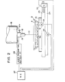
- the apparatus 1 includes a worktank 2 which accommodates a workpiece or substrate 3 which is shown immersed in a chemical-depositing solution 4 which contains a metal to be deposited upon the substrate 3.
- the solution 4 is supplied by a pump (not shown) from a source thereof (not shown) through an inlet pipe 5 into a delivery chamber 6 for temporary storage therein and thence onto a surface of the workpiece 3 through an opening 7 formed at the lower end of the delivery chamber 6. It is desirable that the solution 4 be passed at a high velocity, e.g. between 5 and 25 meters/sec, in the region of the surface of the workpiece 3.
- the workpiece 3 is secured in position by a clamp 8 within the worktank 2.
- the worktank 2 is provided at an upper end portion thereof with a drain outlet 9 to accept the overflowing solution and to feed it to a suitable treatment vessel (not shown).
- the solution delivery chamber 6 is formed with an opening or passage 10 through which a laser beam 11 from a laser beam source or gun 12 is passed to irradiate a localized area on the surface 3a of the workpiece 3.
- the laser gun 12 has a focusing knob 12a for the beam 11 and is carried by a holder 13 which is in turn secured to a support member 14 attached to a semi-circular disk 15.
- the latter is a semi-circular worm wheel rotatably mounted on a head 16 which depends from a spindle 17.
- the worm wheel 15 is rotatable about an axis 18, i.e. a Y-axis, to swing the laser gun 12 and hence the laser beam 11 in an X-Z plane orthogonal to the Y-axis 18.
- the angle of swing is established by the operation of a motor 19 which is drivingly coupled with a worm 20 in mesh with the worm wheel 15. It should be noted that the gun holder 13 or the support member 14 therefor and the solution delivery chamber 6 are mechanically coupled with each other.
- the worktank 2 is securely mounted on a rotary table 21 which is driven by a motor 22 to angularly displace the workpiece 3 in a predetermined polar coordinate system in the X-Y plane.
- the rotary table 21 is in turn carried on X-axis and Y-axis tables 23 and 24 in a cross-slide arrangement to rectilinearly displace the workpiece 3 in the X-Y plane coordinate system.
- the tables 23 and 24 are driven by motors 25 and 26, respectively.
- a control unit 27 is provided to furnish the motors 19, 22, 25 and 26 with respective drive signals based upon preprogrammed data to displace the workpiece 3 so that the laser beam 11 sweeps in a scanning manner with the four degrees of freedom along a predetermined path on the surface thereof.
- the control unit 27 is also stored with velocity commands for the displacement. Furthermore, the beam gun 12 has a parameter setting circuit 28 sequence-controlled by the control unit 27 to sequentially alter the diameter and/or the energy of the irradiating laser beam 11 in accordance with a predetermined program.
- the delivery chamber 6 is furnished with a chemical-depositing solution, e.g. nickel or copper plating solution to deliver it onto the surface of the workpiece 3 at a high velocity as previously indicated.
- a chemical-depositing solution e.g. nickel or copper plating solution to deliver it onto the surface of the workpiece 3 at a high velocity as previously indicated.
- Chemical-depositing conditions including the temperature of the solution, are set up such that without irradiation with a laser beam, deposition takes place uniformly over the workpiece surface 3a and slowly as usual or at a rate much slower than a customarily attainable optimum or highest deposition rate, or even that practically no deposition continues without irradiation with a laser beam.
- FIG. 2 shows an arrangement which is essentially the same as that shown in FIG. 1 except that the solution delivery chamber 6 is dispensed with and the workpiece 3 is immersed in an essentially static mass of the solution 4 retained in the worktank 2.
- the solution may be caused to flow showly between an inlet and an outlet which are formed in the worktank 2 but not shown.
- the laser beam 11 acts as a narrow thermal beam to heat the depositing solution up to a temperature from 45 to 60 °C or higher in the region of a localized area on the workpiece surface 3a through which the solution 4 is forced to flow and that it impinges and thereby selectively activates that interface to enhance the chemical-depositability thereof.
- the focusing knob 12a for the laser beam 11 provided on the gun holder 13 may be used to control the size of the localized activation or depositability-enhanced area on the workpiece surface 3a.
- a pattern of deposition defined by the size of the beam 11 and the path of the relative displacement is created on the workpiece surface 3a.
- the rate of the relative displacement is determined according to the thickness of a deposition pattern desired. Not only is it possible in this manner to achieve a continuous deposition pattern of any shape desired but a set of discontinuous or discrete such patterns is obtainable.
- the control unit 27 operates to turn off the laser source 12 during programmed time intervals in the course of the scanning operation selectively to leave intact those areas which are within the path of the relative displacement but not to be chemically deposited.
- the laser gun 12 may be deactuated selectively during those time intervals or for the corresponding sections of the relative displacement. It is, of course, desirable that minimum time intervals be employed to traverse these sections.
- the method of the invention is useful for producing a print-form circuit or wiring on a board for electronic devices.
- the method is also advantageously used for metal plating or forming on a substrate which is of an intricate contour or has one or more recesses or grooves which could be chemically plated only with difficulty by the conventional technique.
- a metal deposit is achieved uniformly over such a substrate by controlling the time of irradiation or #e the rate of scan with the laser beam 11 or the local point thereof according to the position on the workpiece surface or substrate 3a.
- a recessed area or corner portion in a recess may be irradiated for a longer time than other areas.
- FIG. 3 in which the same reference numerals as those in FIGS. 1 and 2 are used to designate the same or functionally same parts, a modified apparatus embodying the present invention is illustrated.
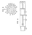
- the apparatus makes use of a relatively large solution delivery chamber 30 in which a plurality of laser irradiation units 31 - 44 (FIG. 4) are accommodated.
- Each of these units of which only 31 - 34 appear in FIG. 3, comprises a laser source 45, 46, 47, 48, Vietnamese connected via a rotary switch 59 to an energization power supply 60 and an optical guide 61, 62, 63, 64, .
- the rotary switch 59 comprises a rotary arm 59a actuated by a switching circuit 90 and arranged for engagement with fixed contacts 91, 92, 93, 94, Vietnamese, which are connected to the laser sources 45, 46, 47, 48, Vietnamese, respectively.
- the switching circuit 90 is operated by the control unit 27 in accordance with a predetermined program stored therein to selectively energize the laser sources 45, 46, 47, 48, « from the power supply 60.
- the control unit 27 also acts on the power supply 60 to control the intensity of the laser beam emitted from each of the sources 45, 46, 47, 48, Vietnamese in accordance with a predetermined stored program.
- the localized areas on the surface 3a of the workpiece 3 are thereby activated and selectively chemically deposited.
- the latter is securely mounted on a slide table 107 with which is drivingly coupled a feed screw 108 extending in the direction normal to the sheet of the drawing to position the workpiece 3 in that direction along a predetermined coordinate axis, i.e. a Y-axis.
- the feed screw 108 is driven by a motor 109 (FIG. 6) which operates in response to drive signals furnished from a control unit 27, e.g. a numerical controller.
- the mirror 111 having its mirror face vertical, is carried on a horizontal support member 112 which is supported on a pedestal 113 so as to be movable horizontally along a predetermined coordinate axis, i.e. an X-axis.
- the support member 112 is carried by a lead screw 114 which is slidably supported on a pedestal 115.
- the lead screw 114 is in mesh with a nut 116 fitted in the center of a large gear 117 in mesh with a small gear 118.
- the latter is carried on the. drive shaft 119a of a motor 119 which operates in response to drive signals furnished from the control unit 27.
- the lead screw 114 is rotated to displace the support member 112 and hence the mirror 111 in the direction of the X-axis to displace the position of the laser beam ; 11 reflected thereby and impinging on the workpiece surface 3a.
- the control unit 27 has path data for relative displacement of the reflected laser beam 11 and the workpiece 3 preprogrammed therein and operates to produce from those data drive signals for the operation of the X-axis motor 119 i and the Y-axis motor 109.
- the solution may, of course, be any conventional chemical depositing solution.
- copper sulfate solution may be used for copper deposition.
- nickel deposition sulfonic nickel solution may be used.
- the laser should preferably be an argon gas laser (having a wavelength between 4880 and 5145 angstroms, green), which has a high transmissivity to such a solution. A beam of the laser can penetrate a solution as thick as 1 to 5 cm and, without substantial heating thereof, is capable of selectively activating a localized area on the workpiece surface to enhance its depositability.
- a carbon-dioxide gas laser (having a wavelength of 10.6 ⁇ m) is relatively low in transmissivity to the solution mentioned and requires that the solution should be present in a thickness as small as 5 mm or less.
- a laser beam from a carbon-dioxide gas laser of 50 watt output can successfully be used to scan a workpiece at a rate of 30 mm/min in deposition of nickel upon the workpiece from a sulfonic nickel chemical-depositing solution when the thickness of the solution on the workpiece os 0.5 mm.
- the solution of that thickness through which the beam travels is then heated up to 60 °C.
- the degree of the localization of deposition is largely reduced.
- the method of the invention is advantageously applicable to printing-type deposition wiring of tiny electronic devices and also to high-precision localized deposition.
- an argon gas laser can be used to provide a beam spot of 0.2 mm diameter and thereby a localized deposition of the same area. This area is increased to 4 mm when the laser is replaced by a carbon-dioxide gas laser.
- an elongate tubular optical guide member 120 is juxtaposed with the surface 3a of a workpiece 3 immersed in the chemical-depositing solution 4 retained in the worktank 2.
- the solution 4 is introduced into the worktank 2 via an inlet conduit 5 and drawn out through a drain outlet 9.
- the elongate tubular guide member 120 has at its lower or forward end a transparent or semi- transparent member 122 fitted therein which may be a plain glass plate as shown at 122a in FIG. 8(A) but is preferably shaped, as shown at 122b in FIG. 8(B), to serve as a convex lens for a laser beam 11 emitted from a laser gun 12.
- the tubular guide member 120 is secured via a coupling ring 123 to the laser gun 12 so that the laser beam emitted from the laser source 12a is passed through the inner bore 121 of the tubular guide member 120 and the transparent or semi-transparent member 122 for irradiation of a localized area on the surface 3a of the workpiece 3.
- the member 122 is designed also to prevent the chemical-depositing solution 4 in the tank 2 from entering into the inner bore 121 of the guide member 120.
- the unit structure comprising the laser gun 12, the annular coupling 123 and the tubular optical guide member 120 in combination is carried by a vertical positioner 124 seated on a wheeled carriage 125.
- the vertical positioner 124 operates in response to drive signals furnished from the control unit 27 to position the forward end of the tubular guide member 120 in closely spaced juxtaposition with the surface 3a of the workpiece 3 which is shown to be planner but may be of an intricate three-dimensional contour.
- the wheeled carriage 125 is displaceable by a motor 126 so as to roll over a track 127 in the direction of the X-axis indicated.
- the track 127 is securely supported on a wheeled carriage 128 with wheels indicated at 129 and 130 and adapted to roll on a pair of rails 131 and 132 to displace the carriage 128 in the direction of the Y-axis indicated.
- the rails 131 and 132 are mounted to stand vertically on the upper edges of the two opposed walls of the worktank 2, respectively and to extend in parallel with each other.
- a motor 133 mounted on the track 127 has on its output shaft a pulley 134 which is coupled via a belt 135 with a pulley 136 secured to the rotary shaft 137 carrying the wheels 129 and 130 for the carriage 128.
- the carriage 128 is thus driven to position the axis of the tubular electrode in the Y-axis coordinate.
- the workpiece 3 may, for example, be a silica board for formation of an electronic circuit thereon.
- the board 3 has been pre-treated according to the conventional techniques, viz. washing, de-greasing with a 10% sodium hydroxide solution, washing, acid-washing with a 3.5% hydrogen chloride solution, washing and drying in sequence.
- the board is then sensitized with a sensitizing agent consisting of 10gr/z SnCl2 and 20 to 50 grit HC1. Thereafter, upon washing, the board is activated at 50 °C with an activating agent composed of 0.5gr/l PdCl 2 which has added thereto HC1 to make its pH 3 to 4 to substitute Sn with Pd which constitutes nuclei for chemical deposition with a desired metal.
- the activated board is then washed and dried.
- the subsequent step of actually depositing the desired metal, say, copper upon the pretreated board may also make use of a known chemical-depositing solution which is, for example, composed of 0.1 mol/cm 3 of (HCHO)n where n is normally 3, 0.05 mol/cm 3 of CuSO 4 and 0.15 mol/cm 3 of EDTA2 Na salt.
- the solution further contains NaOH in an amount to adjust the pH value at 12.5.
- the solution has a temperature of 5°C and is introduced through the inlet 5 into the worktank 2 to flow rapidly in the region of the upper surface of the board 3 so that little deposition of the copper metal from the solution is caused thereon.
- the flowing solution 4 is drained out of the worktank through the outlet 9.
- the laser 12 is actuated to project a laser beam.
- the laser 12 may be an argon laser and the beam intensity adjusted at 15 watts.
- the lens 122b is used to focus the beam so that the beam has a cross section of 15 ⁇ m diameter.
- the laser beam is focused at a localized area on the board surface 3a so that it impinges and thereby selectively activates the interface between the surface 3a and the solution 4 to enhance the chemical-depositability of the localized region.
- a pattern of deposition defined by the size of the laser beam and the path of the relative displacement is created on the board surface 3a.
- deposition proceeds at a rate up to 15 times greater than that obtainable by the conventional technique or without the use of a laser beam.
- the rate of the relative displacement is determined according to the thickness of a deposition pattern desired. Not only is it possible in this manner to achieve a continuous deposition pattern of any shape desired but a set of discontinuous or discrete such patterns is obtainable.
- the control unit 27 operates to turn off the laser source 12a during programmed time intervals in the course of the scanning operation selectively to leave intact those areas which are within the path of the relative displacement but not to be chemically deposited.
- the laser gun 12 may be deactuated selectively during those time intervals or for the corresponding sections of the relative displacement. It is, of course, desirable that minimum time intervals be employed to traverse these sections.
- the solution of the type described be held at a relatively low temperature, e.g. in a range between 3°C to 10 °C, say, at 5°C.
- a suitable cooling means be disposed in contact with the workpiece 3, say, at the rear side thereof to hold it cooled at the low temperature.
- a solution may be held at a relatively high temperature, say, 80 °C.
- the nickel chemical-deposition may be held at room temperature, say, at 20 °C and then no cooling means may be provided.
- FIG. 9 The arrangement of FIG. 9 is the same as in FIG. 7 except that it includes a further provision for measuring the thickness of a deposited layer on the workpiece surface 3a behind the tubular guide member 120.
- a measuring electrode assembly 140 comprising an electrode 141 coated with an insulating film 142, which assembly extends in parallel with the tubular guide member 120 and is carried by its vertical positioner 143 seated on the wheeled carriage 125.
- the vertical positioner 143 operates in response to drive signals furnished from the control unit 27 to position the forward end of the measuring electrode 141 in contact or closely spaced juxtaposition with the deposited workpiece surface 3a. Since the single carriage 125 is used to carry both the tubular guide member 120 and the measuring electrode assembly 140, the axis of the latter is held to be adjacent to the axis of the tubular guide member 120.
- the measuring electrode 141 is adapted to sense its contact or proximate relationship with the deposited workpiece surface 3a by measuring, for example, the electrical resistance therebetween, and to transmit a sensed signal to the control unit 27. The latter continues to furnish drive signals to cause the vertical positioner 125 to advance the measuring electrode assembly 140 until its preselected contact or proximity relationship with the deposited workpiece surface 3a is attained. The distance of advance required may be registered in the control unit 27 to produce control signals which act on the laser gun 12 to control the intensity of the light emitted from the laser source 12a.
- FIG. 10 shows a modification of the embodiment of FIG. 7 and again uses the same reference numerals used therein to indicate the same parts.
- the inner bore 121 of the tubular guide member 120 communi-- cates with a source of pressure gas 145, such as a compressor, via a throttle valve 146 and a pressure-regulating valve 147.
- a source of pressure gas 145 such as a compressor
- the pressure-regulating valve 147 operates in response to command signals furnished from the control circuit 27.
- the control circuit 27 operates to control the pressure-regulating valve 147 so that the pressure of compressed gas within the inner bore 121 of the tubular guide member 120 always exceeds the pressure of the solution 4 in the open end region of the tubular guide member 120 to prevent entry of the solution into the bore 121 thereof.
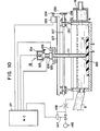
- FIG. 11 shows a laser-assisted chemical-depositing apparatus embodying the present invention and again makes use of the same reference numerals as used in the previous FIGURES to designate the same or functionally same parts.
- a laser gun 12 securely mounted via its holder 13 to a spindle or ram head 17 is designed to project a vertical laser beam 11 for irradiation of a localized area on the workpiece surface 3a therewith.
- a beam-focusing assembly 154 in which a plurality of lenses 155 are arranged.
- the assembly 154 is supported by a horizontal arm 156 which is in turn supported by a vertical lead screw 157 at its lower end.
- the lead screw 157 is in mesh with a nut 158 which is geared on its periphery 159 in mesh with a gear 160 secured to the output shaft of a motor 161.
- the motor 161 is secured to the spindle 17.
- the nut 158 is, for its vertical position to be fixed, retained between a pair of bearing surfaces of a support member 162 secured to the spindle 17.
- the lead screw 157 formed with a key-in groove engaged by a projection 163 on the support member 162 is held against rotation.
- the motor 161 operates in response to drive signals furnished from the control unit 27, e.g. a numerical controller, to position the lens assembly 154 so that the laser beam 11 projected from the laser gun 12 is focused on the localized area on the workpiece surface 3a.
- FIG. 11 is particularly advantageous for chemical-deposition of a workpiece with recessed surfaces or of an intricate contour as shown.
- the control unit 27 provides the motors 22, 25 and 26 with drive signals to displace the workpiece 3 along a preprogrammed path in the X-Y plane so that its surface 3a is swept over by the laser beam 11 from the laser gun 12.
- the motor 161 is responsive to Z-axis positioning signals from the control unit 27 to regulate the position of the lens assembly 154 so as to focus the laser beam 11/localized area.
- the chemical-depositing solution may be a conventional copper chemical-depositing solution held at a relatively low temperature, say, 5°C.
- the solution contain, for example, Ru 2 (b py ) 3 X 2 (obtained by fixing ruthenium to silicate ester of polyvinyl alcohol) in an amount of 2.8 x 10 -6 mol/l.
- the light-beam source 12 can be served by a Xenon lamp.
- the light beam 11 from the Xenon lamp 12 is focused by the lens system 154 into a cross section of 3.5 u diameter as it impinges on the workpiece surface 3a.
- the focused Xenon light beam when used with the solution containing such a sensitizing substance yields A substantially/same rate of chemical deposition as that obtained with an argon laser beam used with the solution omitting the sensitizing substance.
- the laser beam yields a rate of chemical deposition up to three times as great as that obtainable with the Xenon light beam used with the solution containing the sensitizing substance.
Landscapes
- Chemical & Material Sciences (AREA)
- Engineering & Computer Science (AREA)
- Optics & Photonics (AREA)
- Physics & Mathematics (AREA)
- Mechanical Engineering (AREA)
- Chemical Kinetics & Catalysis (AREA)
- Materials Engineering (AREA)
- General Chemical & Material Sciences (AREA)
- Metallurgy (AREA)
- Organic Chemistry (AREA)
- Plasma & Fusion (AREA)
- Manufacturing & Machinery (AREA)
- Microelectronics & Electronic Packaging (AREA)
- Health & Medical Sciences (AREA)
- Toxicology (AREA)
- Electroplating Methods And Accessories (AREA)
- Chemically Coating (AREA)
- Laser Beam Processing (AREA)
- Chemical Vapour Deposition (AREA)
Applications Claiming Priority (2)
| Application Number | Priority Date | Filing Date | Title |
|---|---|---|---|
| JP56160893A JPS5864368A (ja) | 1981-10-12 | 1981-10-12 | 化学メツキ方法 |
| JP160893/81 | 1981-10-12 |
Publications (2)
| Publication Number | Publication Date |
|---|---|
| EP0077207A1 true EP0077207A1 (fr) | 1983-04-20 |
| EP0077207B1 EP0077207B1 (fr) | 1987-04-01 |
Family
ID=15724633
Family Applications (1)
| Application Number | Title | Priority Date | Filing Date |
|---|---|---|---|
| EP82305407A Expired EP0077207B1 (fr) | 1981-10-12 | 1982-10-12 | Procédé et appareil activé par laser pour dépôt chimique |
Country Status (4)
| Country | Link |
|---|---|
| US (1) | US4511595A (fr) |
| EP (1) | EP0077207B1 (fr) |
| JP (1) | JPS5864368A (fr) |
| DE (2) | DE3275934D1 (fr) |
Cited By (2)
| Publication number | Priority date | Publication date | Assignee | Title |
|---|---|---|---|---|
| US4925830A (en) * | 1988-04-14 | 1990-05-15 | Tracer Technologies, Inc. | Laser based method for forming a superconducting oxide layer on various substrates |
| US6459737B1 (en) | 1999-05-07 | 2002-10-01 | Intel Corporation | Method and apparatus for avoiding redundant data retrieval during video decoding |
Families Citing this family (36)
| Publication number | Priority date | Publication date | Assignee | Title |
|---|---|---|---|---|
| FR2542327B1 (fr) * | 1983-03-07 | 1986-03-07 | Bensoussan Marcel | |
| JPS60197879A (ja) * | 1984-03-22 | 1985-10-07 | Nippon Steel Corp | 耐食性のすぐれたステンレス鋼の製造法 |
| JPS6130672A (ja) * | 1984-07-23 | 1986-02-12 | Hitachi Ltd | 選択的加工方法 |
| US4659587A (en) * | 1984-10-11 | 1987-04-21 | Hitachi, Ltd. | Electroless plating process and process for producing multilayer wiring board |
| JPS61231184A (ja) * | 1985-04-08 | 1986-10-15 | Hitachi Ltd | 局所加工装置 |
| JPS6245035A (ja) * | 1985-08-23 | 1987-02-27 | Hitachi Ltd | 半導体装置の製造装置 |
| US5064681A (en) * | 1986-08-21 | 1991-11-12 | International Business Machines Corporation | Selective deposition process for physical vapor deposition |
| DE3686161D1 (de) * | 1986-09-25 | 1992-08-27 | Lucien Diego Laude | Vorrichtung zur laserunterstuetzten, elektrolytischen metallabscheidung. |
| US4938996A (en) * | 1988-04-12 | 1990-07-03 | Ziv Alan R | Via filling by selective laser chemical vapor deposition |
| FR2651508B1 (fr) * | 1989-09-05 | 1994-05-13 | Centre Nal Recherc Scientifique | Dispositif de traitement de pieces par chocs laser. |
| US5405656A (en) * | 1990-04-02 | 1995-04-11 | Nippondenso Co., Ltd. | Solution for catalytic treatment, method of applying catalyst to substrate and method of forming electrical conductor |
| US5292418A (en) * | 1991-03-08 | 1994-03-08 | Mitsubishi Denki Kabushiki Kaisha | Local laser plating apparatus |
| DE4125863A1 (de) * | 1991-08-03 | 1993-02-04 | Lpkf Cad Cam Systeme Gmbh | Verfahren zum aufbringen von strukturierten metallschichten auf glassubstraten |
| US5260108A (en) * | 1992-03-10 | 1993-11-09 | International Business Machines Corporation | Selective seeding of Pd by excimer laser radiation through the liquid |
| US5378508A (en) * | 1992-04-01 | 1995-01-03 | Akzo Nobel N.V. | Laser direct writing |
| WO1994021715A1 (fr) * | 1993-03-23 | 1994-09-29 | Tokai University | Procede et appareil pour modifier une surface solide |
| US6689426B1 (en) * | 1993-03-23 | 2004-02-10 | Tokai University | Solid surface modification method and apparatus |
| US6077617A (en) * | 1998-08-26 | 2000-06-20 | Board Of Regents Of The University Of Nebraska | Rare-earth boride thin film system |
| US6025038A (en) * | 1998-08-26 | 2000-02-15 | Board Of Regents Of The University Of Nebraska | Method for depositing rare-earth boride onto a substrate |
| IL133115A0 (en) * | 1999-11-24 | 2001-03-19 | Yeda Res & Dev | Method for micropatterning of surfaces |
| US6468891B2 (en) * | 2000-02-24 | 2002-10-22 | Micron Technology, Inc. | Stereolithographically fabricated conductive elements, semiconductor device components and assemblies including such conductive elements, and methods |
| GB2381274A (en) * | 2001-10-29 | 2003-04-30 | Qinetiq Ltd | High resolution patterning method |
| GB2385863A (en) * | 2001-10-29 | 2003-09-03 | Qinetiq Ltd | High resolution patterning method |
| RU2267408C2 (ru) * | 2004-02-02 | 2006-01-10 | Сергей Николаевич Максимовский | Способ получения металлизированного изображения на листовом материале и устройство для его осуществления |
| US20050276911A1 (en) * | 2004-06-15 | 2005-12-15 | Qiong Chen | Printing of organometallic compounds to form conductive traces |
| EP1610597A1 (fr) * | 2004-06-22 | 2005-12-28 | Technomedica AG | Précipitation du cuivre pour la fabrication des pistes conductrices |
| DE112007001818T5 (de) * | 2006-08-07 | 2009-06-10 | AUTONETWORKS Technologies, LTD., Yokkaichi | Verfahren zum teilweisen Plattieren, Laserplattiervorrichtung und plattiertes Material |
| CN101823183A (zh) * | 2009-03-04 | 2010-09-08 | 鸿富锦精密工业(深圳)有限公司 | 水导激光装置 |
| CN101864587B (zh) * | 2009-04-20 | 2013-08-21 | 鸿富锦精密工业(深圳)有限公司 | 纳米级金属粒子/金属复合镀层的形成装置及形成方法 |
| JP2011111355A (ja) * | 2009-11-25 | 2011-06-09 | Ricoh Co Ltd | 薄膜製造方法および薄膜素子 |
| EP2541673A1 (fr) * | 2010-02-25 | 2013-01-02 | Tokyo Electron Limited | Appareil de fabrication et procédé de fabrication de cellule solaire à colorant |
| JP5865601B2 (ja) * | 2011-04-28 | 2016-02-17 | 株式会社リコー | 強誘電体膜の製造方法及び強誘電体膜の製造装置 |
| DE112014005277T5 (de) * | 2014-06-12 | 2016-10-06 | Fuji Electric Co., Ltd. | Vorrichtung zum Einbringen von Verunreinigungen, Verfahren zum Einbringen von Verunreinigungen und Verfahren zur Herstellung eines Halbleiterelements |
| US11158502B2 (en) * | 2014-09-25 | 2021-10-26 | Purdue Research Foundation | Methods of forming nano-scale and micro-scale structured materials and materials formed thereby |
| US10590541B2 (en) * | 2018-06-15 | 2020-03-17 | Rohm And Haas Electronic Materials Llc | Electroless copper plating compositions and methods for electroless plating copper on substrates |
| US11168400B2 (en) | 2018-06-21 | 2021-11-09 | International Business Machines Corporation | Formation of terminal metallurgy on laminates and boards |
Citations (4)
| Publication number | Priority date | Publication date | Assignee | Title |
|---|---|---|---|---|
| US4217183A (en) * | 1979-05-08 | 1980-08-12 | International Business Machines Corporation | Method for locally enhancing electroplating rates |
| US4239789A (en) * | 1979-05-08 | 1980-12-16 | International Business Machines Corporation | Maskless method for electroless plating patterns |
| WO1981001529A1 (fr) * | 1979-11-30 | 1981-06-11 | Brasilia Telecom | Procede de depot de vapeur chimique avec chauffage au laser |
| US4281030A (en) * | 1980-05-12 | 1981-07-28 | Bell Telephone Laboratories, Incorporated | Implantation of vaporized material on melted substrates |
Family Cites Families (3)
| Publication number | Priority date | Publication date | Assignee | Title |
|---|---|---|---|---|
| JPS5092830A (fr) * | 1973-12-20 | 1975-07-24 | ||
| US4233368A (en) * | 1978-06-05 | 1980-11-11 | United States Gypsum Company | Method for the production of glass fiber-reinforced gypsum sheets and gypsum board formed therefrom |
| US4359485A (en) * | 1981-05-01 | 1982-11-16 | Bell Telephone Laboratories, Incorporated | Radiation induced deposition of metal on semiconductor surfaces |
-
1981
- 1981-10-12 JP JP56160893A patent/JPS5864368A/ja active Granted
-
1982
- 1982-10-12 DE DE8282305407T patent/DE3275934D1/de not_active Expired
- 1982-10-12 DE DE198282305407T patent/DE77207T1/de active Pending
- 1982-10-12 EP EP82305407A patent/EP0077207B1/fr not_active Expired
-
1984
- 1984-06-01 US US06/616,793 patent/US4511595A/en not_active Expired - Fee Related
Patent Citations (4)
| Publication number | Priority date | Publication date | Assignee | Title |
|---|---|---|---|---|
| US4217183A (en) * | 1979-05-08 | 1980-08-12 | International Business Machines Corporation | Method for locally enhancing electroplating rates |
| US4239789A (en) * | 1979-05-08 | 1980-12-16 | International Business Machines Corporation | Maskless method for electroless plating patterns |
| WO1981001529A1 (fr) * | 1979-11-30 | 1981-06-11 | Brasilia Telecom | Procede de depot de vapeur chimique avec chauffage au laser |
| US4281030A (en) * | 1980-05-12 | 1981-07-28 | Bell Telephone Laboratories, Incorporated | Implantation of vaporized material on melted substrates |
Cited By (2)
| Publication number | Priority date | Publication date | Assignee | Title |
|---|---|---|---|---|
| US4925830A (en) * | 1988-04-14 | 1990-05-15 | Tracer Technologies, Inc. | Laser based method for forming a superconducting oxide layer on various substrates |
| US6459737B1 (en) | 1999-05-07 | 2002-10-01 | Intel Corporation | Method and apparatus for avoiding redundant data retrieval during video decoding |
Also Published As
| Publication number | Publication date |
|---|---|
| JPS5864368A (ja) | 1983-04-16 |
| DE3275934D1 (en) | 1987-05-07 |
| US4511595A (en) | 1985-04-16 |
| EP0077207B1 (fr) | 1987-04-01 |
| DE77207T1 (de) | 1983-11-10 |
| JPH0213027B2 (fr) | 1990-04-03 |
Similar Documents
| Publication | Publication Date | Title |
|---|---|---|
| US4511595A (en) | Laser-activated chemical-depositing method and apparatus | |
| US4430165A (en) | Laser-activated electrodepositing method and apparatus | |
| EP0734325B1 (fr) | Imagerie ablative par lithographie de proximite | |
| CN109926584B (zh) | 一种增材制造和表面抛光同步加工方法及装置 | |
| CN110312583B (zh) | 通过激光热处理、特别是通过熔合的用于增材制造的激光操作机器以及对应方法 | |
| US3736402A (en) | Automated laser tool | |
| US20110042201A1 (en) | In situ Plating And Soldering Of Materials Covered With A Surface Film | |
| CN205309586U (zh) | 一种飞秒激光加工航空发动机叶片气膜孔的装置 | |
| WO1991012120A1 (fr) | Procede et appareil de formation d'un article tridimensionnel solide a partir d'un milieu liquide | |
| US4972798A (en) | Drawing machine | |
| JPS5921491A (ja) | レ−ザ−加工ロボット | |
| CN101269441A (zh) | 激光柔性加工系统 | |
| CA3239966A1 (fr) | Dispositif laser et son utilisation, et procede de traitement d'une feuille de verre | |
| KR960008696B1 (ko) | 와이어커트 방전가공기 | |
| EP1099183A1 (fr) | Systeme d'apport de matiere pour fabrication de structure miniature | |
| JP2022536957A (ja) | レーザ走査ヘッドによって方向づけられたレーザビームおよび横方向粉末射出によって加工物の定められた表面に材料を付加するシステムおよび方法 | |
| JPH02504238A (ja) | レーザー光線により皮膜を除去する方法及び装置 | |
| CN111745158A (zh) | 增材制造方法 | |
| CN119658397B (zh) | 一种切削装置及切削方法 | |
| CN115464150A (zh) | 用于金属增材制造的激光熔丝沉积设备及方法 | |
| CN113573488B (zh) | 激光和化学结合选择性活化绝缘材料制造导电图案的系统 | |
| JPH02108519A (ja) | 三次元形状の形成方法および装置 | |
| JPH04218676A (ja) | 金属層の無電解堆積方法 | |
| CN224073559U (zh) | 一种激光加工装置 | |
| CN223194928U (zh) | 一种电路增材制造装置 |
Legal Events
| Date | Code | Title | Description |
|---|---|---|---|
| PUAI | Public reference made under article 153(3) epc to a published international application that has entered the european phase |
Free format text: ORIGINAL CODE: 0009012 |
|
| AK | Designated contracting states |
Designated state(s): DE FR GB IT |
|
| ITCL | It: translation for ep claims filed |
Representative=s name: FIAMMENGHI FIAMMENGHI RACHELI |
|
| 17P | Request for examination filed |
Effective date: 19830309 |
|
| EL | Fr: translation of claims filed | ||
| DET | De: translation of patent claims | ||
| ITF | It: translation for a ep patent filed | ||
| GRAA | (expected) grant |
Free format text: ORIGINAL CODE: 0009210 |
|
| AK | Designated contracting states |
Kind code of ref document: B1 Designated state(s): DE FR GB IT |
|
| REF | Corresponds to: |
Ref document number: 3275934 Country of ref document: DE Date of ref document: 19870507 |
|
| ET | Fr: translation filed | ||
| PLBE | No opposition filed within time limit |
Free format text: ORIGINAL CODE: 0009261 |
|
| STAA | Information on the status of an ep patent application or granted ep patent |
Free format text: STATUS: NO OPPOSITION FILED WITHIN TIME LIMIT |
|
| 26N | No opposition filed | ||
| PGFP | Annual fee paid to national office [announced via postgrant information from national office to epo] |
Ref country code: GB Payment date: 19890930 Year of fee payment: 8 |
|
| PGFP | Annual fee paid to national office [announced via postgrant information from national office to epo] |
Ref country code: DE Payment date: 19891021 Year of fee payment: 8 |
|
| PGFP | Annual fee paid to national office [announced via postgrant information from national office to epo] |
Ref country code: FR Payment date: 19891031 Year of fee payment: 8 |
|
| PG25 | Lapsed in a contracting state [announced via postgrant information from national office to epo] |
Ref country code: GB Effective date: 19901012 |
|
| GBPC | Gb: european patent ceased through non-payment of renewal fee | ||
| PG25 | Lapsed in a contracting state [announced via postgrant information from national office to epo] |
Ref country code: FR Effective date: 19910628 |
|
| PG25 | Lapsed in a contracting state [announced via postgrant information from national office to epo] |
Ref country code: DE Effective date: 19910702 |
|
| REG | Reference to a national code |
Ref country code: FR Ref legal event code: ST |