EP0077253A1 - Sicherheitsanordnung zwischen dem Steuersystem eines Sicherheitsstellantriebes und einer zugehörigen logischen Steuerschaltung - Google Patents
Sicherheitsanordnung zwischen dem Steuersystem eines Sicherheitsstellantriebes und einer zugehörigen logischen Steuerschaltung Download PDFInfo
- Publication number
- EP0077253A1 EP0077253A1 EP82401803A EP82401803A EP0077253A1 EP 0077253 A1 EP0077253 A1 EP 0077253A1 EP 82401803 A EP82401803 A EP 82401803A EP 82401803 A EP82401803 A EP 82401803A EP 0077253 A1 EP0077253 A1 EP 0077253A1
- Authority
- EP
- European Patent Office
- Prior art keywords
- signals
- logic
- logic circuit
- transmission
- failure
- Prior art date
- Legal status (The legal status is an assumption and is not a legal conclusion. Google has not performed a legal analysis and makes no representation as to the accuracy of the status listed.)
- Granted
Links
Images
Classifications
-
- G—PHYSICS
- G21—NUCLEAR PHYSICS; NUCLEAR ENGINEERING
- G21D—NUCLEAR POWER PLANT
- G21D3/00—Control of nuclear power plant
- G21D3/04—Safety arrangements
-
- G—PHYSICS
- G05—CONTROLLING; REGULATING
- G05B—CONTROL OR REGULATING SYSTEMS IN GENERAL; FUNCTIONAL ELEMENTS OF SUCH SYSTEMS; MONITORING OR TESTING ARRANGEMENTS FOR SUCH SYSTEMS OR ELEMENTS
- G05B9/00—Safety arrangements
- G05B9/02—Safety arrangements electric
-
- G—PHYSICS
- G06—COMPUTING OR CALCULATING; COUNTING
- G06F—ELECTRIC DIGITAL DATA PROCESSING
- G06F11/00—Error detection; Error correction; Monitoring
- G06F11/07—Responding to the occurrence of a fault, e.g. fault tolerance
- G06F11/0703—Error or fault processing not based on redundancy, i.e. by taking additional measures to deal with the error or fault not making use of redundancy in operation, in hardware, or in data representation
- G06F11/0751—Error or fault detection not based on redundancy
-
- G—PHYSICS
- G06—COMPUTING OR CALCULATING; COUNTING
- G06F—ELECTRIC DIGITAL DATA PROCESSING
- G06F11/00—Error detection; Error correction; Monitoring
- G06F11/07—Responding to the occurrence of a fault, e.g. fault tolerance
- G06F11/0796—Safety measures, i.e. ensuring safe condition in the event of error, e.g. for controlling element
-
- G—PHYSICS
- G06—COMPUTING OR CALCULATING; COUNTING
- G06F—ELECTRIC DIGITAL DATA PROCESSING
- G06F11/00—Error detection; Error correction; Monitoring
- G06F11/07—Responding to the occurrence of a fault, e.g. fault tolerance
- G06F11/14—Error detection or correction of the data by redundancy in operations
- G06F11/1402—Saving, restoring, recovering or retrying
- G06F11/1405—Saving, restoring, recovering or retrying at machine instruction level
- G06F11/141—Saving, restoring, recovering or retrying at machine instruction level for bus or memory accesses
-
- G—PHYSICS
- G08—SIGNALLING
- G08C—TRANSMISSION SYSTEMS FOR MEASURED VALUES, CONTROL OR SIMILAR SIGNALS
- G08C25/00—Arrangements for preventing or correcting errors; Monitoring arrangements
-
- Y—GENERAL TAGGING OF NEW TECHNOLOGICAL DEVELOPMENTS; GENERAL TAGGING OF CROSS-SECTIONAL TECHNOLOGIES SPANNING OVER SEVERAL SECTIONS OF THE IPC; TECHNICAL SUBJECTS COVERED BY FORMER USPC CROSS-REFERENCE ART COLLECTIONS [XRACs] AND DIGESTS
- Y02—TECHNOLOGIES OR APPLICATIONS FOR MITIGATION OR ADAPTATION AGAINST CLIMATE CHANGE
- Y02E—REDUCTION OF GREENHOUSE GAS [GHG] EMISSIONS, RELATED TO ENERGY GENERATION, TRANSMISSION OR DISTRIBUTION
- Y02E30/00—Energy generation of nuclear origin
Definitions
- the invention relates to a safety device between a control system for safety actuators and a logic circuit for controlling these actuators. It applies in particular to tests of transmission systems and means which make it possible to apply emergency trigger signals to a safety actuator. These safety actuators are used, for example, to control the emergency shutdown of a nuclear reactor.
- a nuclear reactor for example, includes a large number of devices which make it possible to control its operation. These devices are qualified as safety actuators. In the event of an incident, these actuators must be able to be triggered urgently, so that their protective action can stop this incident.
- the values of a certain number of physical quantities such as pressure, temperature, neutron flux, etc., are measured at a certain number of points, using sensors. The analog values of these quantities are converted into digital values which are then compared in processing systems, with reference values. These processing systems also make it possible to control one or more safety actuators.
- a logic comparison signal which is, for example, of non-zero value, when the numerical values of the physical quantities are situated in a range of reference values defined in advance and corresponding to the normal operation of the apparatus or of the reactor under surveillance.
- the processing and communication system (s) mande delivers logic output signals of zero value, for example, for each of the measurement values outside the safety range.
- this logic circuit is designed so that a protective action is triggered when at least half of the redundant channels of the communication means apply to at least half of the inputs of this logic circuit signals for triggering control signals. protective actions.
- These logic circuits also make it possible, as indicated in French patent application No. 80 25068 filed on November 26, 1980 in the name of the same applicant, to inhibit some of the transmission channels, to carry out tests, for example, circuits or system located upstream of these tracks.
- These circuits located upstream can be, for example, amplification and signal processing chains, connected to the sensors mentioned above.
- the aim of the present invention is to remedy these drawbacks and in particular to produce a safety device between a control system for a safety actuator and a logic control circuit for this actuator, this device making it possible, simply and permanently, to verify that the logic signals sent by the system to the logic circuit are transmitted without failure, and to verify that the control system itself does not exhibit any failure.
- the invention relates to a safety device between a system for controlling safety actuators and a logic circuit for controlling these actuators, characterized in that it comprises sequential means for transmitting logic signals emitted by the system of command to the logic circuit, sequential verification means, to apply actuator trigger signals to the logic circuit, in the event of a failure of the control system or in the event of failure of the transmission means, the transmission of the signals between the system and the logic circuit being carried out after verification of the non-failure of the transmission means.
- the verification means comprise timing means connected between the system and the transmission means, a clock for controlling these timing means, the transmission means applying trigger signals to the logic circuit. of the actuator, in the event of a system failure, if after a predetermined time interval the delay means have not received a reset signal from the system, these means verification further comprising means for comparing the signals emitted by the system and signals from the transmission means, so that in the event of a difference between these signals, an output of the comparison means applies an error signal to the system for that the latter does not apply a reset signal to the delay means, after the predetermined time interval, the transmission means thus applying to the logic circuit actuator trigger signals.
- the comparison means are limited to means for re-reading by the. system, the state of the signals applied to the logic circuit. The comparison of the signals emitted by the system and of the signals coming from the transmission means then being carried out by the system itself.
- the timing means consist of a counter, the output of which is in a first logic state for a determined period corresponding to the verification of the non-failure of the system and of the transmission means and to the transmission of the logic signals transmitted by the system, this output then being in a second logic state during said predetermined time interval corresponding to the time which elapses between on the one hand, the instant of switching from the first logic state to the second logic state and, from on the other hand, the instant when the system applies said reset signal to this counter.
- said predetermined time interval has a duration less than the response time of the logic circuit.
- the transmission means comprise a plurality of transmission channels transmission connecting inputs of the logic circuit with outputs of a register receiving the logic signals emitted by the system, each channel comprising two controllable switches, connected in series between an output of the register and an input of the logic circuit, the first switch being controlled by the logic level of the signal emitted by the system and coming from the corresponding output of the register, the second switch being controlled by the signal from the output of the counter, so as to be open during said predetermined time interval, or in the event of failure .
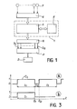
- FIG. 1 schematically represents a security assembly in which a security device according to the invention operates.
- This security assembly comprises a system 1 which makes it possible to control safety actuators 2, by means of a logic control circuit 3.
- the control system 1 can be constituted for example by a processor or a microprocessor 4, associated to a memory 5.
- This microprocessor receives for example, via an interface 6, measurement signals from from sensors 7.
- These measurement signals are generally analog signals which are transformed by circuits (not shown), inside the interface 6, into digital values.
- the digital measurement values are compared with reference values relating to each of the measurement signals, recorded in memory 5. If digital values representative of the measurement signals are located outside of digital safety ranges, the control system 1 provides for these values, to logic circuit 3, logic signals for commanding the triggering of urgent action of the actuator 2.
- this urgent action is only triggered if a certain number of redundant logic signals which reach the inputs of logic circuit 3, are at a logic level corresponding to an urgent action triggering command.
- this logic level is a low logic level: absence of voltage.
- the device of the invention is shown at 8 in this figure. This logic device makes it possible, as will be seen below in detail, to ensure a sequential transmission of the logic signals emitted by the control system 1, to the logic circuit 3. This device also makes it possible to apply signals to this logic circuit actuator 2 trigger in the event of failure of the control systems 1 or in the event of failure of the transmission means (shown diagrammatically by the channels S 1 , ... S 8 ).
- These transmission means are constituted by several channels relating to different protection actions and the device of the invention makes it possible to trigger an urgent action in the event of failure of one or more of the channels.
- these transmission channels can also transmit logic signals for triggering the actuator. 2, apart from any failure of the control system or of the transmission means.
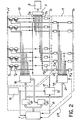
- FIG. 2 shows, in more detail, the security device according to the invention.
- This safety device comprises sequential means 10 for transmitting the logic signals emitted by the control system 1 to the logic circuit 3.
- This device also includes sequential verification means 11, which make it possible to apply signals to the logic circuit 3. triggering of the actuator (not shown), in the event of failure of the control system 1 or in the event of failure of the transmission means 10.
- the verification means 11 comprise means, for timing 12 constituted by a counter whose role will be explained later in detail. These verification means also include a clock 13 which controls the counter 12 and which also makes it possible to synchronize the control system 1. Finally, these verification means include re-reading means 14 allowing re-reading, by system 1 of the state , corresponding logic signals S l , ... S 8 , coming from the transmission means 10. As will be seen below, these verification means make it possible to apply to the logic circuit 3, actuator trigger signals, in the event of system 1 failure, if after a predetermined time interval, the delay means constituted by the counter 12 have not received a reset signal R from the system.
- the replay means 14 are replaced by comparison means which apply to the system 1 an error signal ER in the case where the signals emitted by the system and the signals received by the logic circuit are discordant.
- the error signal ER acts on the system 1 so that the latter does not apply a reset signal R to the delay means 12, after a predetermined time interval.
- the counter 12 is a counter which can be reset and whose output 15 is in a logic state 1 for a period which corresponds to the transmission of the signals emitted by the system 1, to the verification of the non-failure of the system and of the non failure of the transmission means 10.
- the output of this counter then switches to a logic state 0.
- This second logic state is present for a predetermined time interval which corresponds to the time which elapses between on the one hand, the instant of switching from the first logic state to the second logic state and, on the other hand, the instant when the system 1 applies to this counter the reset signal R.
- the transmission of logic signals from the system to the communication channels can only be carried out if transistors such as T 2 belonging to the communication means which will be described later in detail, are turned on. These transistors are turned on when a logic level 1 is applied to their bases. The transmission of the logic signals emitted by the system 1 is therefore carried out during the determined period which corresponds to the production of a signal having a logic state 1 on the output 15 of the counter 12.
- the second logic state of the output 15 of the counter 12 is a logic level 0 which blocks transistors such as T 2 and which therefore makes it impossible to transmit logic signals from the control system to logic circuit 3.
- This logic level 0 corresponds to the application of trip signals to the inputs of the logic circuit 3.
- the predetermined time interval mentioned above is less than the response time of logic circuit 3.
- the transmission means 10 comprise a plurality of transmission channels, the outputs of which are shown in S 1 , ... S 8 and the number of which is equal to 8 in the embodiment described, this number of course being able to be different.
- These transmission channels connect the inputs of the logic circuit 3 with outputs of a register 18 which receives the logic signals transmitted by the system 1, for example by means of a command decoder 19 and a decoder d places 20.
- Each transmission channel comprises two switches which are connected in series between an output of the register 18 and a corresponding input of the logic circuit 3. These switches are realized by transistors, such that Tl and T 2. In the embodiment considered, these transistors are of PNP type.
- the collector of transistor T 1 is connected to the emitter of transistor T 2 , while the emitter of transistor T 1 is brought to a bias voltage + V; the collector of transistor T 2 is connected to a reference ground M via a resistor R 2 .
- the bases of the transistors T 2 are connected to the output 15 of the counter 12, while the bases of the transistors T 1 are connected to the corresponding outputs of the register 18.
- the first switches constituted by the transistors T 1 are controlled by the signals correspondents from register 18, while the second switches constituted by the transistors T 2 are controlled by the signal from the output 15 of the counter 12.
- the transistors T 2 are blocked for the predetermined time interval mentioned above, or in case of failure, as will be seen below in detail.
- the replay means 14 which allow the comparison by the system of the signals received by the logic circuit 3, receive these signals on their inputs 21 and present them on their outputs 22; the signals received by the logic circuits 3 are applied to the inputs 22 of the replay device 14, via a divider bridge adapter with resistors, such as R 3 , R 4 .
- This comparator is synchronized by the processor 4 of the control system 1.
- FIG. 3 is a timing diagram which represents, in a and b, the logic states of the output 15 of the counter 12 in two cases of operation of the device.
- the counter adjustable 12 controlled by the clock 13 provides at the output signals C 1 of determined period t l .
- These signals present a first logic state 1 and it is during this period that the logic signals transmitted by the control system 1 are transmitted and that the non-failure of the system 1 and of the communication means 10 is then verified for the transmission of the logic signals of the following sequence.
- the output 15 of the counter 12 is at a logic level 1. This logic level makes it possible to turn on the second switches constituted by the transistors T 2 .
- the control system 1 When there is no failure of the processing system 1 or of the transmission means 10, after a predetermined time interval t 2 , the control system 1, synchronized with the clock 13, applies the signal to the counter 12 reset R. This signal makes it possible to control the counter so that its output 15 again returns to a logic state 1 for a new period of duration t l .
- Case b corresponds to a failure, either of the control system 1, or of the communication means 10. It is considered here that the transmission of the logic signals from the system to the logic circuit 3, has been carried out normally until now ⁇ 1 for switching the output of counter 12 to logic level 0. In the event of failure of the control system 1, the latter does not provide, at time ⁇ 2 , after the predetermined time interval t 2 , which separates this instant G 2 from the instant ⁇ 1 at which the counter output had switched, a reset signal R. It follows that the counter output then remains in the logic state O, and that the second switches constituted by the transistors T 2 are open (blocked transistors); this corresponds to the application of logic signals 0 to the inputs of logic circuit 3, these signals causing the actuator to trip.
- the process is identical during a failure of the communication means 10. Indeed, during a failure of these communication means, the system 1 acquires, via the replay device 14, the state of the signals applied to the logic circuit, detects a discrepancy between the signals which it emitted and those which it re-reads and under these conditions no longer controls the emission of the reset signal R, after the time interval t 2 . It therefore follows, as previously, that the output 15 of the counter 12 remains in a logic state 0, beyond this time interval t 2 , which causes the application of trigger signals to the inputs of the logic circuit 3 actuator control 2.
- the transmission means 10 make it possible to transmit trigger signals coming from the control system 1, apart from any failure of this system or any failure of the transmission means 10.
- the counter 12 provides many logic signals such as C 1 , of logic level 1, but since the signals applied to the transistors T1 are at a logic level 0 corresponding to the failure command, and the outputs SI to S 8 of the device are at a logic level O corresponding to actuator 2 tripping.
Landscapes
- Engineering & Computer Science (AREA)
- Physics & Mathematics (AREA)
- General Physics & Mathematics (AREA)
- Theoretical Computer Science (AREA)
- General Engineering & Computer Science (AREA)
- Quality & Reliability (AREA)
- Automation & Control Theory (AREA)
- Plasma & Fusion (AREA)
- High Energy & Nuclear Physics (AREA)
- Emergency Management (AREA)
- Business, Economics & Management (AREA)
- Safety Devices In Control Systems (AREA)
- Fluid-Pressure Circuits (AREA)
- Testing And Monitoring For Control Systems (AREA)
Applications Claiming Priority (2)
| Application Number | Priority Date | Filing Date | Title |
|---|---|---|---|
| FR8119028 | 1981-10-09 | ||
| FR8119028A FR2514522A1 (fr) | 1981-10-09 | 1981-10-09 | Dispositif de securite entre un systeme de commande d'un actionneur de surete et un circuit logique de commande de cet actionneur |
Publications (2)
| Publication Number | Publication Date |
|---|---|
| EP0077253A1 true EP0077253A1 (de) | 1983-04-20 |
| EP0077253B1 EP0077253B1 (de) | 1986-02-05 |
Family
ID=9262886
Family Applications (1)
| Application Number | Title | Priority Date | Filing Date |
|---|---|---|---|
| EP82401803A Expired EP0077253B1 (de) | 1981-10-09 | 1982-10-04 | Sicherheitsanordnung zwischen dem Steuersystem eines Sicherheitsstellantriebes und einer zugehörigen logischen Steuerschaltung |
Country Status (6)
| Country | Link |
|---|---|
| EP (1) | EP0077253B1 (de) |
| JP (1) | JPS58127202A (de) |
| KR (1) | KR890000024B1 (de) |
| DE (1) | DE3268980D1 (de) |
| FR (1) | FR2514522A1 (de) |
| ZA (1) | ZA827146B (de) |
Citations (4)
| Publication number | Priority date | Publication date | Assignee | Title |
|---|---|---|---|---|
| US3919533A (en) * | 1974-11-08 | 1975-11-11 | Westinghouse Electric Corp | Electrical fault indicator |
| US4090173A (en) * | 1976-12-17 | 1978-05-16 | General Signal Corporation | Vital digital communication system |
| EP0011312A1 (de) * | 1977-07-09 | 1980-05-28 | LUCAS INDUSTRIES public limited company | Elektrische Einrichtungen für Strassenfahrzeuge |
| DE2946081A1 (de) * | 1979-11-15 | 1981-05-27 | Wabco Fahrzeugbremsen Gmbh, 3000 Hannover | Anordnung zur ueberwachung der funktion eines programmierbaren elektronischen schaltkreises |
Family Cites Families (1)
| Publication number | Priority date | Publication date | Assignee | Title |
|---|---|---|---|---|
| JPS52147288A (en) * | 1976-06-02 | 1977-12-07 | Hitachi Ltd | Misoperation prevention equipment |
-
1981
- 1981-10-09 FR FR8119028A patent/FR2514522A1/fr active Granted
-
1982
- 1982-09-29 ZA ZA827146A patent/ZA827146B/xx unknown
- 1982-10-04 DE DE8282401803T patent/DE3268980D1/de not_active Expired
- 1982-10-04 EP EP82401803A patent/EP0077253B1/de not_active Expired
- 1982-10-07 JP JP57176933A patent/JPS58127202A/ja active Pending
- 1982-10-08 KR KR8204542A patent/KR890000024B1/ko not_active Expired
Patent Citations (4)
| Publication number | Priority date | Publication date | Assignee | Title |
|---|---|---|---|---|
| US3919533A (en) * | 1974-11-08 | 1975-11-11 | Westinghouse Electric Corp | Electrical fault indicator |
| US4090173A (en) * | 1976-12-17 | 1978-05-16 | General Signal Corporation | Vital digital communication system |
| EP0011312A1 (de) * | 1977-07-09 | 1980-05-28 | LUCAS INDUSTRIES public limited company | Elektrische Einrichtungen für Strassenfahrzeuge |
| DE2946081A1 (de) * | 1979-11-15 | 1981-05-27 | Wabco Fahrzeugbremsen Gmbh, 3000 Hannover | Anordnung zur ueberwachung der funktion eines programmierbaren elektronischen schaltkreises |
Also Published As
| Publication number | Publication date |
|---|---|
| FR2514522A1 (fr) | 1983-04-15 |
| KR840002122A (ko) | 1984-06-11 |
| FR2514522B1 (de) | 1984-03-16 |
| ZA827146B (en) | 1983-07-27 |
| KR890000024B1 (ko) | 1989-03-06 |
| DE3268980D1 (en) | 1986-03-20 |
| EP0077253B1 (de) | 1986-02-05 |
| JPS58127202A (ja) | 1983-07-29 |
Similar Documents
| Publication | Publication Date | Title |
|---|---|---|
| CH669057A5 (fr) | Installation de surveillance et d'alarme. | |
| FR2606897A1 (fr) | Procede et dispositif pour surveiller les organes de reglage commandes par un calculateur, comme par exemple des systemes anti-blocage, des poches d'air ou des tendeurs de ceintures ou analogues | |
| EP0504062A1 (de) | Integrierte Schaltung mit servogesteuerten Impedanzen und Anwendung für Senderempfänger, insbesondere für die Kommunikation zwischen Einheiten eines Informationssystems | |
| FR2692379A1 (fr) | Procédé de détention et de passivation de pannes dans un système de traitement de données, et système de traitement de données adapté à sa mise en Óoeuvre. | |
| FR2477738A1 (fr) | Appareil de commande et de controle destine a etre utilise entre un poste central de calculateur et des postes terminaux | |
| FR2459484A1 (fr) | Detecteur de defaillance pour filtre a cristal | |
| CH636211A5 (fr) | Detecteur de feu discriminant par comptage d'impulsions. | |
| EP0667533A2 (de) | Signalverlustdetektor | |
| EP0094279A1 (de) | Verfahren zum Schutz eines Fernüberwachungssystemes gegen Sabotage und System zur Ausführung dieses Verfahrens | |
| FR2653278A1 (fr) | Horloge synchronisee. | |
| EP0504063A1 (de) | Sender-Empfänger für gleichzeitige, bidirektionelle Datenübertragung im Basisband | |
| EP0077253A1 (de) | Sicherheitsanordnung zwischen dem Steuersystem eines Sicherheitsstellantriebes und einer zugehörigen logischen Steuerschaltung | |
| FR2563026A1 (fr) | Dispositif de controle pour des amplificateurs d'attaque integres | |
| FR2566211A1 (fr) | Convertisseur analogique-numerique par approximations successives | |
| EP2327160B1 (de) | Analogzähler und ein einen solchen zähler enthaltenden bildgeber | |
| FR2494877A1 (fr) | Systeme logique de securite pour declencher l'action de protection d'un actionneur de surete | |
| EP0112429B1 (de) | System zur Übertragung von Daten durch sich wiederholende Folgen | |
| FR2575014A1 (fr) | Recepteur de signaux admettant un derangement | |
| US4524449A (en) | Safety device | |
| CA1205893A (fr) | Interface pour relier un systeme informatique a un dispositif actionneur | |
| EP0193453B1 (de) | Anordnung zur Überwachung der Impulsperiodendauer | |
| FR2488763A1 (fr) | Systeme de detection et d'annulation d'image fantome de television, controle sur plusieurs lignes d'un intervalle de retour vertical | |
| EP0133840A1 (de) | Programmierbares Gerät für ein Industrieverfahren das gegen Industriegeräusche geschützt ist | |
| FR2638268A1 (fr) | Dispositifs pour permettre de discriminer entre plusieurs phenomenes simultanes | |
| SU1598184A2 (ru) | Устройство контрол цифровых световодных систем передачи информации |
Legal Events
| Date | Code | Title | Description |
|---|---|---|---|
| PUAI | Public reference made under article 153(3) epc to a published international application that has entered the european phase |
Free format text: ORIGINAL CODE: 0009012 |
|
| AK | Designated contracting states |
Designated state(s): BE DE FR GB IT |
|
| 17P | Request for examination filed |
Effective date: 19830808 |
|
| ITF | It: translation for a ep patent filed | ||
| GRAA | (expected) grant |
Free format text: ORIGINAL CODE: 0009210 |
|
| AK | Designated contracting states |
Designated state(s): BE DE FR GB IT |
|
| REF | Corresponds to: |
Ref document number: 3268980 Country of ref document: DE Date of ref document: 19860320 |
|
| PLBE | No opposition filed within time limit |
Free format text: ORIGINAL CODE: 0009261 |
|
| STAA | Information on the status of an ep patent application or granted ep patent |
Free format text: STATUS: NO OPPOSITION FILED WITHIN TIME LIMIT |
|
| 26N | No opposition filed | ||
| REG | Reference to a national code |
Ref country code: FR Ref legal event code: TP |
|
| ITTA | It: last paid annual fee | ||
| PGFP | Annual fee paid to national office [announced via postgrant information from national office to epo] |
Ref country code: GB Payment date: 19951002 Year of fee payment: 14 Ref country code: BE Payment date: 19951002 Year of fee payment: 14 |
|
| PGFP | Annual fee paid to national office [announced via postgrant information from national office to epo] |
Ref country code: DE Payment date: 19951019 Year of fee payment: 14 |
|
| PG25 | Lapsed in a contracting state [announced via postgrant information from national office to epo] |
Ref country code: GB Effective date: 19961004 |
|
| PG25 | Lapsed in a contracting state [announced via postgrant information from national office to epo] |
Ref country code: BE Effective date: 19961031 |
|
| BERE | Be: lapsed |
Owner name: FRAMATOME ET CIE Effective date: 19961031 Owner name: COMMISSARIAT A L'ENERGIE ATOMIQUE ETABLISSEMENT D Effective date: 19961031 |
|
| GBPC | Gb: european patent ceased through non-payment of renewal fee |
Effective date: 19961004 |
|
| PG25 | Lapsed in a contracting state [announced via postgrant information from national office to epo] |
Ref country code: DE Effective date: 19970701 |
|
| PGFP | Annual fee paid to national office [announced via postgrant information from national office to epo] |
Ref country code: FR Payment date: 19981030 Year of fee payment: 17 |
|
| PG25 | Lapsed in a contracting state [announced via postgrant information from national office to epo] |
Ref country code: FR Free format text: LAPSE BECAUSE OF NON-PAYMENT OF DUE FEES Effective date: 20000630 |
|
| REG | Reference to a national code |
Ref country code: FR Ref legal event code: ST |