EP0077445A2 - Procédé de réalisation d'une structure de circuit électronique - Google Patents
Procédé de réalisation d'une structure de circuit électronique Download PDFInfo
- Publication number
- EP0077445A2 EP0077445A2 EP82107379A EP82107379A EP0077445A2 EP 0077445 A2 EP0077445 A2 EP 0077445A2 EP 82107379 A EP82107379 A EP 82107379A EP 82107379 A EP82107379 A EP 82107379A EP 0077445 A2 EP0077445 A2 EP 0077445A2
- Authority
- EP
- European Patent Office
- Prior art keywords
- pattern
- radiation
- microcircuit
- resist
- thin film
- Prior art date
- Legal status (The legal status is an assumption and is not a legal conclusion. Google has not performed a legal analysis and makes no representation as to the accuracy of the status listed.)
- Granted
Links
Images


Classifications
-
- G—PHYSICS
- G03—PHOTOGRAPHY; CINEMATOGRAPHY; ANALOGOUS TECHNIQUES USING WAVES OTHER THAN OPTICAL WAVES; ELECTROGRAPHY; HOLOGRAPHY
- G03F—PHOTOMECHANICAL PRODUCTION OF TEXTURED OR PATTERNED SURFACES, e.g. FOR PRINTING, FOR PROCESSING OF SEMICONDUCTOR DEVICES; MATERIALS THEREFOR; ORIGINALS THEREFOR; APPARATUS SPECIALLY ADAPTED THEREFOR
- G03F7/00—Photomechanical, e.g. photolithographic, production of textured or patterned surfaces, e.g. printing surfaces; Materials therefor, e.g. comprising photoresists; Apparatus specially adapted therefor
- G03F7/70—Microphotolithographic exposure; Apparatus therefor
- G03F7/70425—Imaging strategies, e.g. for increasing throughput or resolution, printing product fields larger than the image field or compensating lithography- or non-lithography errors, e.g. proximity correction, mix-and-match, stitching or double patterning
-
- G—PHYSICS
- G03—PHOTOGRAPHY; CINEMATOGRAPHY; ANALOGOUS TECHNIQUES USING WAVES OTHER THAN OPTICAL WAVES; ELECTROGRAPHY; HOLOGRAPHY
- G03F—PHOTOMECHANICAL PRODUCTION OF TEXTURED OR PATTERNED SURFACES, e.g. FOR PRINTING, FOR PROCESSING OF SEMICONDUCTOR DEVICES; MATERIALS THEREFOR; ORIGINALS THEREFOR; APPARATUS SPECIALLY ADAPTED THEREFOR
- G03F7/00—Photomechanical, e.g. photolithographic, production of textured or patterned surfaces, e.g. printing surfaces; Materials therefor, e.g. comprising photoresists; Apparatus specially adapted therefor
- G03F7/004—Photosensitive materials
- G03F7/09—Photosensitive materials characterised by structural details, e.g. supports, auxiliary layers
- G03F7/095—Photosensitive materials characterised by structural details, e.g. supports, auxiliary layers having more than one photosensitive layer
- G03F7/0957—Photosensitive materials characterised by structural details, e.g. supports, auxiliary layers having more than one photosensitive layer with sensitive layers on both sides of the substrate
-
- G—PHYSICS
- G03—PHOTOGRAPHY; CINEMATOGRAPHY; ANALOGOUS TECHNIQUES USING WAVES OTHER THAN OPTICAL WAVES; ELECTROGRAPHY; HOLOGRAPHY
- G03F—PHOTOMECHANICAL PRODUCTION OF TEXTURED OR PATTERNED SURFACES, e.g. FOR PRINTING, FOR PROCESSING OF SEMICONDUCTOR DEVICES; MATERIALS THEREFOR; ORIGINALS THEREFOR; APPARATUS SPECIALLY ADAPTED THEREFOR
- G03F7/00—Photomechanical, e.g. photolithographic, production of textured or patterned surfaces, e.g. printing surfaces; Materials therefor, e.g. comprising photoresists; Apparatus specially adapted therefor
- G03F7/20—Exposure; Apparatus therefor
- G03F7/2022—Multi-step exposure, e.g. hybrid; backside exposure; blanket exposure, e.g. for image reversal; edge exposure, e.g. for edge bead removal; corrective exposure
-
- H—ELECTRICITY
- H05—ELECTRIC TECHNIQUES NOT OTHERWISE PROVIDED FOR
- H05K—PRINTED CIRCUITS; CASINGS OR CONSTRUCTIONAL DETAILS OF ELECTRIC APPARATUS; MANUFACTURE OF ASSEMBLAGES OF ELECTRICAL COMPONENTS
- H05K3/00—Apparatus or processes for manufacturing printed circuits
- H05K3/0073—Masks not provided for in groups H05K3/02 - H05K3/46, e.g. for photomechanical production of patterned surfaces
- H05K3/0082—Masks not provided for in groups H05K3/02 - H05K3/46, e.g. for photomechanical production of patterned surfaces characterised by the exposure method of radiation-sensitive masks
-
- H—ELECTRICITY
- H10—SEMICONDUCTOR DEVICES; ELECTRIC SOLID-STATE DEVICES NOT OTHERWISE PROVIDED FOR
- H10P—GENERIC PROCESSES OR APPARATUS FOR THE MANUFACTURE OR TREATMENT OF DEVICES COVERED BY CLASS H10
- H10P76/00—Manufacture or treatment of masks on semiconductor bodies, e.g. by lithography or photolithography
- H10P76/20—Manufacture or treatment of masks on semiconductor bodies, e.g. by lithography or photolithography of masks comprising organic materials
- H10P76/204—Manufacture or treatment of masks on semiconductor bodies, e.g. by lithography or photolithography of masks comprising organic materials of organic photoresist masks
- H10P76/2045—Electron beam lithography processes
-
- H—ELECTRICITY
- H05—ELECTRIC TECHNIQUES NOT OTHERWISE PROVIDED FOR
- H05K—PRINTED CIRCUITS; CASINGS OR CONSTRUCTIONAL DETAILS OF ELECTRIC APPARATUS; MANUFACTURE OF ASSEMBLAGES OF ELECTRICAL COMPONENTS
- H05K2201/00—Indexing scheme relating to printed circuits covered by H05K1/00
- H05K2201/01—Dielectrics
- H05K2201/0104—Properties and characteristics in general
- H05K2201/0108—Transparent
-
- H—ELECTRICITY
- H05—ELECTRIC TECHNIQUES NOT OTHERWISE PROVIDED FOR
- H05K—PRINTED CIRCUITS; CASINGS OR CONSTRUCTIONAL DETAILS OF ELECTRIC APPARATUS; MANUFACTURE OF ASSEMBLAGES OF ELECTRICAL COMPONENTS
- H05K2203/00—Indexing scheme relating to apparatus or processes for manufacturing printed circuits covered by H05K3/00
- H05K2203/15—Position of the PCB during processing
- H05K2203/1572—Processing both sides of a PCB by the same process; Providing a similar arrangement of components on both sides; Making interlayer connections from two sides
-
- H—ELECTRICITY
- H05—ELECTRIC TECHNIQUES NOT OTHERWISE PROVIDED FOR
- H05K—PRINTED CIRCUITS; CASINGS OR CONSTRUCTIONAL DETAILS OF ELECTRIC APPARATUS; MANUFACTURE OF ASSEMBLAGES OF ELECTRICAL COMPONENTS
- H05K3/00—Apparatus or processes for manufacturing printed circuits
- H05K3/02—Apparatus or processes for manufacturing printed circuits in which the conductive material is applied to the surface of the insulating support and is thereafter removed from such areas of the surface which are not intended for current conducting or shielding
- H05K3/04—Apparatus or processes for manufacturing printed circuits in which the conductive material is applied to the surface of the insulating support and is thereafter removed from such areas of the surface which are not intended for current conducting or shielding the conductive material being removed mechanically, e.g. by punching
- H05K3/046—Apparatus or processes for manufacturing printed circuits in which the conductive material is applied to the surface of the insulating support and is thereafter removed from such areas of the surface which are not intended for current conducting or shielding the conductive material being removed mechanically, e.g. by punching by selective transfer or selective detachment of a conductive layer
- H05K3/048—Apparatus or processes for manufacturing printed circuits in which the conductive material is applied to the surface of the insulating support and is thereafter removed from such areas of the surface which are not intended for current conducting or shielding the conductive material being removed mechanically, e.g. by punching by selective transfer or selective detachment of a conductive layer using a lift-off resist pattern or a release layer pattern
-
- H—ELECTRICITY
- H05—ELECTRIC TECHNIQUES NOT OTHERWISE PROVIDED FOR
- H05K—PRINTED CIRCUITS; CASINGS OR CONSTRUCTIONAL DETAILS OF ELECTRIC APPARATUS; MANUFACTURE OF ASSEMBLAGES OF ELECTRICAL COMPONENTS
- H05K3/00—Apparatus or processes for manufacturing printed circuits
- H05K3/02—Apparatus or processes for manufacturing printed circuits in which the conductive material is applied to the surface of the insulating support and is thereafter removed from such areas of the surface which are not intended for current conducting or shielding
- H05K3/06—Apparatus or processes for manufacturing printed circuits in which the conductive material is applied to the surface of the insulating support and is thereafter removed from such areas of the surface which are not intended for current conducting or shielding the conductive material being removed chemically or electrolytically, e.g. by photo-etch process
- H05K3/061—Etching masks
- H05K3/064—Photoresists
Definitions
- This invention relates to a method of forming electronic circuit structures of submicron size.
- Microminiature electronic devices are fabricated and largely interconnected using lithographic techniques. In successive steps, thin patterned layers of desired material are formed on top of each other to build up a desired multilayer integrated electronic structure. Each component layer of an integrated electronic circuit typically is patterned differently.
- a resist layer is used to pattern a component layer. The resist layer itself is patterned first by exposing it to a desired pattern of actinic radiation and then developing (preferentially etching away) either the exposed regions (positive resist) or the unexposed regions (negative resist).
- the patterned resist layer acts-as a mask during deposition of the component layer.
- the patterned resist layer acts as an etching mask to pattern a previously deposited underlying component layer.
- the patterned resist layer normally must be removed before the next component layer is formed on top using another resist layer.
- Characteristic of this process is the need to realign each exposure pattern with previously formed component layer patterns.
- Realignment of the multilayer structure is needed before patternwise exposure of each individual resist layer (except possibly the first one) because there are process steps between successive pattern exposures which require removal of the multilayer structure from the exposure tool (e.g. resist layer development, resist removal, resist deposition, component layer etching, etc.).
- Realignment is typically done by aligning each exposure pattern with respect to alignment marks on the multilayer structure.
- the accuracy of these realignments is particularly critical when active devices are being formed by several successive component layers. Even small misalignments can affect device characteristics. This problem becomes even more severe as the physical size of the active devices is reduced.
- a patterned component layer is a pattern of regions where the layer material is absent. The surface thus is very uneven.
- the next layer to be deposited should result again in a substantially flat surface. This tends to happen better when the next layer is relatively thick.
- pattern resolution in the next layer is typically reduced as the thickness of the layer is increased.
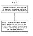
- a method of forming a microcircuit structure characterised in that the method comprises the steps of defining a first microcircuit pattern on one side of a thin film substrate with radiation incident upon said one side and defining a second microcircuit pattern on the opposite side of said thin film substrate with radiation which is incident also upon said one side but which passes through said thin film substrate to define said second microcircuit pattern on said opposite side, said microcircuit patterns both being defined without any intermediate realignment of said thin film substrate.
- the same radiation pattern defines microcircuit patterns on both sides of the thin substrate simultaneously.
- different radiation patterns are used to define the respective microcircuit patterns on each side.
- the two sides of the thin substrate may not be simultaneously sensitive to the same radiation pattern. This is done either by making the character of the two radiation patterns different or by sensitizing only one side of the substrate at a time to patterning radiation.
- the preferred patterning radiation is electron beam radiation and the preferred method of defining the microcircuit patterns is with contamination resist. Controlled deposition of contamination resist by electron beam onto only one side of a thin substrate at a time is done by supplying contamination material to only one side of the substrate at a time.
- ultra-small multilayer microcircuit structures having self-aligned patterned layers can be fabricated by taking advantage of the ability of patterning radiation to pass completely through thin material layers in order to define a lithographic pattern on the opposite side of a thin supporting membrane or substrate.
- the supporting membrane or substrate becomes the central layer of an active device formed by lithographically patterning layers situated on opposite sides of the supporting membrane or substrate.
- Thin supporting membranes or "window" substrates which may be used in practicing this invention are described, for example, in U.S. Patent 3,971,860, "High Resolution Electron Beam Fabrication Using STEM", Proc. Ninth Int. Cong. on Electron Microscopy, Toronto, Vol. 3, pp. 343-354 (1978) and in A.N. Broers et al, "High Resolution Electron Beam Lithography and Applications to Superconducting Devices", 44 Amer. Inst. Phys. P roc. 289 (1978).
- a window substrate is formed, for example, by coating a silicon wafer with a thin film and then preferentially etching the silicon away to leave a window covered with a thin film membrane.
- Preferred membranes consist of silicon nitride or oxide of 200 to 2000A thickness.
- a supporting membrane or substrate 10 is coated on the top side with a layer 12 and on the bottom side with a layer 14.
- the materials of layers 10, 12, 14 are selected in accordance with the materials and thicknesses desired in a final device structure.
- a resist layer 16 is deposited and on top of layer 14 (physically below it) a second resist layer 18 is deposited. This whole structure is then irradiated with a desired pattern of actinic radiation 20 (here represented by a single beam 21).
- the pattern of radiation may be created through use of a mask (projection contact or proximity type or by writing with a fine beam (raster scan or vector scan).
- the radiation may be any type of particle beam, such as an electron beam or ion beam, or any type of electromagnetic radiation, such as visible light, ultraviolet light, or x-ray radiation.
- the radiation pattern 20 passes completely through the multilayer structure exposing a corresponding pattern 22 in resist layer 16 and a corresponding pattern 24 in resist layer 18. It should be appreciated that some scattering and focussing differences can be expected between resist layers 16 and 18 in practice, so that the exposed patterns 22, 24 should not be expected to be exactly identical in a practical multilayer structure of this type. For the purpose of illustration, however, patterns 22, 24 are shown to be virtually identical.
- resist layers 16, 18 are both sensitive to at least one radiation component of the radiation pattern, but that resist layer 16 is negative acting and that resist layer 18 is positive acting.
- resist layer 16 has been removed everywhere except in the subareas 22 which have been irradiated to form a first resist pattern 26, while resist layer 18 has been removed only in the subareas which have been irradiated to form a second pattern 28 which is substantially complementary to resist pattern 26.
- This structure next is subjected to an etchant which removes layers 12 and 14 everywhere not protected by an overlying resist layer. It is not necessary that both sides be etched simultaneously nor that both sides be etched in the same manner.
- a preferred method of etching is through use of an ion beam.
- FIG. 1.3 results.
- a first microcircuit pattern 30 has been formed corresponding to resist pattern 26 and a second microcircuit pattern 32 has been formed corresponding to resist pattern 28.
- Microcircuit patterns 30, 32 are substantially complementary.
- the resist layers now may be completely removed with a suitable solvent to produce the device structure illustrated in FIG. 1.4. It should be noted that two microcircuit patterns 30, 32 which are substantially complementary have been formed in opposite sides of an intermediate layer 10.
- microcircuit devices such as field effect transistors.
- Both microcircuit patterns have been defined by the same radiation source (in fact the same radiation pattern) and without any need for intermediate realignment.
- further microcircuit layers could be added to one or both sides in subsequent steps if desired.
- the thin membrane substrates currently available in the art are rather fragile so that further two sided lithography may not be practical until less fragile membrane substrates are developed. If no further lithography is required, the resist layers obviously need not be removed.
- FIG. 2 illustrates the end structure which results instead when resist layers 16 and 18 are both negative acting.
- the microcircuit patterns 34, 36 in this case are substantially identical and automatically self aligned with each other. Certain microcircuit device structures also have this geometrical configuration, such as tunnel junction devices.
- FIG. 3 illustrates the use of a mask 38 to produce a radiation pattern 40 incident upon and passing through the multilayer structure first illustrated in FIG. 1.1.
- Mask 38 may be in contact with the multilayer structure, or it may be close to it but not touching (proximity mask), or it may be far away from the multilayer structure (projection mask).
- one or more lens elements might be interposed between the mask and multilayer structure for the purpose of imaging the mask onto the multilayer structure.
- a filter 39 may be interposed between the thin film multilayer structure 38 and the radiation source 41 to alter an energy characteristic of the radiation emitted from the source.
- control leads 43 may control, for example, the temperature of an electromagnetic energy radiating body (and consequently the emission spectrum) or an acceleration voltage in the case of a charged particle beam.
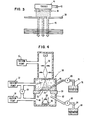
- FIG. 4 illustrates an apparatus for double sided lithography with contamination resist.
- a thin membrane 50 covers an etched window 52 in a silicon support 54. Fabrication of such a structure is described, for example, in the previously cited references.
- This "window" substrate is mounted within an electron beam chamber 56 in a position such that the electron beam 58 can strike the membrane.
- the chamber space 60 above the membrane is separated from the chamber space 62 below the membrane in any convenient manner. In the illustration, the top and bottom parts are separated by the window substrate itself. It should be understood that in practice window substrates are much smaller than illustrated so that separate partitioning means would be used instead.
- top chamber space 60 and the bottom chamber space 62 are not connected within the chamber 56, separate pump out ports 64, 66 communicate with the chamber spaces 60, 62.
- a valve 68 is opened during evacuation to equalize pressure in the chamber spaces.
- Vacuum pumps 70, 72, 74 are used to evacuate the whole electron beam chamber 56. Obviously, one or two vacuum pumps could be used instead since all of the evacuated spaces are connected (at least while valve 68 is open).
- a first source 76 of carbonaceous vapour 78 communicates with the upper chamber 60 via a valve 80.
- a second source 82 of carbonaceous vapour 84 communicates with the lower chamber 62 via a valve 86.
- a heating element 88 and reflector 90 are positioned to apply heat to the membrane 50.
- Double sided lithography is carried out with the apparatus shown in FIG. 4 in the following manner.
- the upper and lower chambers are evacuated.
- heat may be applied to the membrane to drive off contaminants.
- carbonaceous vapour is supplied to one side of the membrane.
- FIG. 4 shows vapour being supplied to the upper chamber only.
- Valve 68 may be closed if pressure equalization is not needed. If the vacuum pumps are operating, it is expected that valve 68 would need to be open for pressure equalization. In any event, vapour is not supplied to the other side of the membrane or permitted to reach the other side.
- electron beam 58 writes a first pattern.
- the procedure is repeated with respect to the other side of the membrane to form another contamination resist pattern.
- the vapour on the side where the first contamination resist pattern was formed is removed. This may be done in part with the vacuum pump system assisted by some membrane heating. It is also possible to merely turn off the vapour supply using the associated valve and then to deplete the residual vapour by directing the electron beam to an unused region of the membrane for a time sufficient to use up or deposit all of the vapour on that side.
- a second pattern is written by the electron beam. This time the carbonaceous material deposits on the other side and not on the first side to selectively form a second contamination resist pattern only on the other side.
- FIGS. 5.1 - 5.4 show a membrane in cross section at various points in this process.
- the membrane 50 has been coated on the top side with a layer 92 and on the bottom side with a layer 94 in preparation for later etching similar to what was described in connection with FIGS. 1.1 - 1.4.
- a first contamination resist pattern 96 is deposited only on the top side by supplying vapour only to the top side during irradiation with a first electron beam pattern (FIG. 5.1).
- a second contamination resist pattern 98 is deposited only on the bottom side by supplying vapour only to the bottom side during irradiation with a second electron beam pattern (FIG. 5.2).
- both sides are etched so that layers 92, 94 are removed everywhere except those regions protected by contamination resist (FIG. 5.3). If practical techniques are developed for removing contamination resist, it can be removed then, if desired, to produce the structure shown in F IG. 5.4.
- top and bottom patterns independently of each other (they need not be identical or complementary) and no intermediate realignment of the membrane is needed because the membrane has not been removed from the vacuum chamber between the first and second pattern defining steps.
- similar or identical contamination resist patterns can be written simultaneously, if desired, by supplying vapour to both sides simultaneously. This is illustrated in FIG. 6.1.
- the resulting final microcircuit structure (after removing the contamination resist) is illustrated in FIG. 6.2.
- the character of the source radiation could be different during exposure of the two sides.
- contamination resist could be deposited on one side with an electron beam and a resist pattern could be optically exposed on the other side.
- one or both of the microcircuit patterns may be formed from a resist pattern by using a lift-off process rather than a subtractive etching process.
- the layer next to the supporting film or membrane is a resist layer rather than a microcircuit layer.
- a resist layer is deposited on top of the resist pattern and the resist pattern is dissolved away to "lift-off" the parts of the microcircuit layer which lie on top of the resist.
- the resist layer thus produces a complementary pattern in the microcircuit layer.
- Other variations or modifications should also be apparent in which double sided lithography can be performed without any intermediate realignment of the lithography workpiece between the top and bottom pattern defining steps.
- the general method is illustrated in block diagram in FIG. 7.
Landscapes
- Engineering & Computer Science (AREA)
- Physics & Mathematics (AREA)
- General Physics & Mathematics (AREA)
- Architecture (AREA)
- Structural Engineering (AREA)
- Manufacturing & Machinery (AREA)
- Microelectronics & Electronic Packaging (AREA)
- Electron Beam Exposure (AREA)
- Exposure And Positioning Against Photoresist Photosensitive Materials (AREA)
- Exposure Of Semiconductors, Excluding Electron Or Ion Beam Exposure (AREA)
- Preparing Plates And Mask In Photomechanical Process (AREA)
Applications Claiming Priority (2)
| Application Number | Priority Date | Filing Date | Title |
|---|---|---|---|
| US311831 | 1981-10-16 | ||
| US06/311,831 US4557995A (en) | 1981-10-16 | 1981-10-16 | Method of making submicron circuit structures |
Publications (3)
| Publication Number | Publication Date |
|---|---|
| EP0077445A2 true EP0077445A2 (fr) | 1983-04-27 |
| EP0077445A3 EP0077445A3 (en) | 1986-05-07 |
| EP0077445B1 EP0077445B1 (fr) | 1988-07-27 |
Family
ID=23208689
Family Applications (1)
| Application Number | Title | Priority Date | Filing Date |
|---|---|---|---|
| EP82107379A Expired EP0077445B1 (fr) | 1981-10-16 | 1982-08-13 | Procédé de réalisation d'une structure de circuit électronique |
Country Status (5)
| Country | Link |
|---|---|
| US (1) | US4557995A (fr) |
| EP (1) | EP0077445B1 (fr) |
| JP (1) | JPS5873122A (fr) |
| CA (1) | CA1204882A (fr) |
| DE (1) | DE3278837D1 (fr) |
Cited By (6)
| Publication number | Priority date | Publication date | Assignee | Title |
|---|---|---|---|---|
| EP0226449A3 (en) * | 1985-12-11 | 1988-10-05 | International Business Machines Corporation | Apparatus and method for calculating parameters of print head drive system for printer |
| EP0318037A3 (fr) * | 1987-11-27 | 1990-07-25 | Sony Corporation | Méthode pour l'obtention de textures très fines en utilisant une couche texturée résistante |
| EP0361460A3 (fr) * | 1988-09-29 | 1990-08-01 | Sony Corporation | Méthode pour la fabrication d'un motif |
| US5171718A (en) * | 1987-11-27 | 1992-12-15 | Sony Corporation | Method for forming a fine pattern by using a patterned resist layer |
| WO2008120915A1 (fr) | 2007-03-30 | 2008-10-09 | Lg Chem, Ltd. | Procédé de fabrication d'un film ayant un micro-motif sur celui-ci et film fabriqué par celui-ci |
| WO2020050726A1 (fr) * | 2018-09-06 | 2020-03-12 | Callaghan Innovation | Appareil et procédé de fabrication d'un article à l'aide d'une photolithographie et d'une photorésine |
Families Citing this family (15)
| Publication number | Priority date | Publication date | Assignee | Title |
|---|---|---|---|---|
| GB8714177D0 (en) * | 1987-06-17 | 1987-07-22 | Grace W R Ltd | Printing plate manufacture |
| US4898804A (en) * | 1988-03-31 | 1990-02-06 | Cornell Research Foundation | Self-aligned, high resolution resonant dielectric lithography |
| US5040020A (en) * | 1988-03-31 | 1991-08-13 | Cornell Research Foundation, Inc. | Self-aligned, high resolution resonant dielectric lithography |
| US5298988A (en) * | 1992-06-02 | 1994-03-29 | Massachusetts Institute Of Technology | Technique for aligning features on opposite surfaces of a substrate |
| US5452166A (en) * | 1993-10-01 | 1995-09-19 | Applied Magnetics Corporation | Thin film magnetic recording head for minimizing undershoots and a method for manufacturing the same |
| US6034752A (en) * | 1997-03-22 | 2000-03-07 | Kent Displays Incorporated | Display device reflecting visible and infrared radiation |
| FR2858876B1 (fr) * | 2003-08-12 | 2006-03-03 | St Microelectronics Sa | Procede de formation sous une couche mince d'un premier materiau de portions d'un autre materiau et/ou de zones de vide |
| US8298754B2 (en) * | 2003-11-25 | 2012-10-30 | Murata Manufacturing Co., Ltd. | Method for forming thick film pattern, method for manufacturing electronic component, and photolithography photosensitive paste |
| WO2006076036A2 (fr) * | 2004-05-25 | 2006-07-20 | The Trustees Of The University Of Pennsylvania | Ensembles de nanostructures, procedes et dispositifs |
| US20060066803A1 (en) * | 2004-09-30 | 2006-03-30 | Aylward Peter T | Substrate free flexible liquid crystal displays |
| WO2006119251A2 (fr) | 2005-04-29 | 2006-11-09 | University Of Rochester | Membranes nanoporeuses ultrafines, procede de fabrication et leurs utilisations |
| US7922795B2 (en) * | 2005-04-29 | 2011-04-12 | University Of Rochester | Ultrathin nanoscale membranes, methods of making, and uses thereof |
| JP2009529888A (ja) * | 2006-03-14 | 2009-08-27 | ユニバーシティ オブ ロチェスター | 超薄多孔質メンブレンを有する細胞培養装置およびその使用 |
| FR2921751B1 (fr) * | 2007-10-02 | 2009-12-18 | St Microelectronics Crolles 2 | Procede de realisation de dispositif semi-conducteur a architecture asymetrique |
| JP5703865B2 (ja) * | 2011-03-14 | 2015-04-22 | セイコーエプソン株式会社 | 液体噴射ヘッドの製造方法 |
Family Cites Families (8)
| Publication number | Priority date | Publication date | Assignee | Title |
|---|---|---|---|---|
| DE1095665B (de) * | 1959-01-12 | 1960-12-22 | Hans Hoerner | Verfahren zur fotomechanischen Herstellung von Hochdruckformen aus mehreren Kunststoffschichten |
| US3264105A (en) * | 1962-05-31 | 1966-08-02 | Western Electric Co | Method of using a master art drawing to produce a two-sided printed circuit board |
| US3313626A (en) * | 1962-08-01 | 1967-04-11 | Russeli H Whitney | Process of making a lithographic printing plate |
| DE2115823C3 (de) * | 1971-04-01 | 1975-09-18 | Licentia Patent-Verwaltungs-Gmbh, 6000 Frankfurt | Verfahren zum Herstellen von Mikrostrukturen auf einer Halbleiterscheibe |
| US3971860A (en) * | 1973-05-07 | 1976-07-27 | International Business Machines Corporation | Method for making device for high resolution electron beam fabrication |
| US3964908A (en) * | 1975-09-22 | 1976-06-22 | International Business Machines Corporation | Positive resists containing dimethylglutarimide units |
| FR2470393A1 (fr) * | 1979-11-19 | 1981-05-29 | Labo Electronique Physique | Procede de realisation d'une structure planaire a grande frequence spatiale et de grande longueur |
| US4371598A (en) * | 1981-07-06 | 1983-02-01 | Motorola, Inc. | Method for fabricating aligned patterns on the opposed surfaces of a transparent substrate |
-
1981
- 1981-10-16 US US06/311,831 patent/US4557995A/en not_active Expired - Fee Related
-
1982
- 1982-08-05 JP JP57135811A patent/JPS5873122A/ja active Granted
- 1982-08-13 EP EP82107379A patent/EP0077445B1/fr not_active Expired
- 1982-08-13 DE DE8282107379T patent/DE3278837D1/de not_active Expired
- 1982-10-06 CA CA000412957A patent/CA1204882A/fr not_active Expired
Cited By (8)
| Publication number | Priority date | Publication date | Assignee | Title |
|---|---|---|---|---|
| EP0226449A3 (en) * | 1985-12-11 | 1988-10-05 | International Business Machines Corporation | Apparatus and method for calculating parameters of print head drive system for printer |
| EP0318037A3 (fr) * | 1987-11-27 | 1990-07-25 | Sony Corporation | Méthode pour l'obtention de textures très fines en utilisant une couche texturée résistante |
| US5171718A (en) * | 1987-11-27 | 1992-12-15 | Sony Corporation | Method for forming a fine pattern by using a patterned resist layer |
| US5147823A (en) * | 1988-09-20 | 1992-09-15 | Sony Corporation | Method for forming an ultrafine metal pattern using an electron beam |
| EP0361460A3 (fr) * | 1988-09-29 | 1990-08-01 | Sony Corporation | Méthode pour la fabrication d'un motif |
| WO2008120915A1 (fr) | 2007-03-30 | 2008-10-09 | Lg Chem, Ltd. | Procédé de fabrication d'un film ayant un micro-motif sur celui-ci et film fabriqué par celui-ci |
| EP2135120A4 (fr) * | 2007-03-30 | 2010-03-31 | Lg Chemical Ltd | Procédé de fabrication d'un film ayant un micro-motif sur celui-ci et film fabriqué par celui-ci |
| WO2020050726A1 (fr) * | 2018-09-06 | 2020-03-12 | Callaghan Innovation | Appareil et procédé de fabrication d'un article à l'aide d'une photolithographie et d'une photorésine |
Also Published As
| Publication number | Publication date |
|---|---|
| EP0077445B1 (fr) | 1988-07-27 |
| CA1204882A (fr) | 1986-05-20 |
| DE3278837D1 (en) | 1988-09-01 |
| EP0077445A3 (en) | 1986-05-07 |
| JPS6219054B2 (fr) | 1987-04-25 |
| US4557995A (en) | 1985-12-10 |
| JPS5873122A (ja) | 1983-05-02 |
Similar Documents
| Publication | Publication Date | Title |
|---|---|---|
| EP0077445B1 (fr) | Procédé de réalisation d'une structure de circuit électronique | |
| JP4065200B2 (ja) | インサイチュリソグラフィマスククリーニング | |
| WO1980000639A1 (fr) | Fabrication d'un circuit integre utilisant des modeles epais a haute resolution | |
| JPS596506B2 (ja) | 電子写真製版方法 | |
| JP2007521645A (ja) | インプリント・リソグラフィによる単一デュアルダマシン製法 | |
| Schattenburg et al. | Fabrication of high-energy x-ray transmission gratings for the Advanced X-ray Astrophysics Facility (AXAF) | |
| KR20050032581A (ko) | 갭 결함을 가진 리소그라픽 템플릿을 형성하고 수리하는방법 | |
| US20050130074A1 (en) | Method for the manufacture of micro structures | |
| CA1157575A (fr) | Reduction de l'effet de chargement en lithographie aux rayons ionises | |
| KR20250086596A (ko) | 포토리소그래피 방법 및 포토리소그래피 시스템 | |
| US7820343B2 (en) | Method for producing a photomask, method for patterning a layer or layer stack and resist stack on a mask substrate | |
| EP4506757A1 (fr) | Dispositif de lithographie utilisant une couche électronique dans un système sous vide | |
| US4122335A (en) | Method and apparatus for mask to wafer gap control in X-ray lithography | |
| US5759722A (en) | Electron beam aperture structure and method for fabricating the same | |
| EP0104235A4 (fr) | Procede de formation d'un materiau de protection lithographique hybride a rayon electronique/optique. | |
| US12400822B2 (en) | Particle transfer blocking device and lithography device using electron layer in vacuum system | |
| JP3605485B2 (ja) | フオトマスク用エッチング装置 | |
| US20260082870A1 (en) | Method and apparatus for in-situ dry development | |
| US20230005737A1 (en) | Method of manufacturing a semiconductor device | |
| KR20230143795A (ko) | 진공 시스템에서 정전 트랩을 구비한 전자층을 이용한 입자 이동 차단 장치 및 리소그래피 장치 | |
| JPH05303210A (ja) | パターン形成方法 | |
| KR100244765B1 (ko) | 반도체 소자의 미세 패턴 방법 | |
| KR19990042757A (ko) | 반도체 소자의 미세 패턴 형성방법 | |
| JPS63244622A (ja) | 半導体装置の製造方法 | |
| JPS646448B2 (fr) |
Legal Events
| Date | Code | Title | Description |
|---|---|---|---|
| PUAI | Public reference made under article 153(3) epc to a published international application that has entered the european phase |
Free format text: ORIGINAL CODE: 0009012 |
|
| AK | Designated contracting states |
Designated state(s): DE FR GB IT |
|
| 17P | Request for examination filed |
Effective date: 19830823 |
|
| PUAL | Search report despatched |
Free format text: ORIGINAL CODE: 0009013 |
|
| AK | Designated contracting states |
Kind code of ref document: A3 Designated state(s): DE FR GB IT |
|
| 17Q | First examination report despatched |
Effective date: 19870429 |
|
| GRAA | (expected) grant |
Free format text: ORIGINAL CODE: 0009210 |
|
| AK | Designated contracting states |
Kind code of ref document: B1 Designated state(s): DE FR GB IT |
|
| REF | Corresponds to: |
Ref document number: 3278837 Country of ref document: DE Date of ref document: 19880901 |
|
| ET | Fr: translation filed | ||
| ITF | It: translation for a ep patent filed | ||
| PLBE | No opposition filed within time limit |
Free format text: ORIGINAL CODE: 0009261 |
|
| STAA | Information on the status of an ep patent application or granted ep patent |
Free format text: STATUS: NO OPPOSITION FILED WITHIN TIME LIMIT |
|
| 26N | No opposition filed | ||
| ITTA | It: last paid annual fee | ||
| PGFP | Annual fee paid to national office [announced via postgrant information from national office to epo] |
Ref country code: GB Payment date: 19920722 Year of fee payment: 11 |
|
| PGFP | Annual fee paid to national office [announced via postgrant information from national office to epo] |
Ref country code: FR Payment date: 19920724 Year of fee payment: 11 |
|
| PGFP | Annual fee paid to national office [announced via postgrant information from national office to epo] |
Ref country code: DE Payment date: 19920822 Year of fee payment: 11 |
|
| PG25 | Lapsed in a contracting state [announced via postgrant information from national office to epo] |
Ref country code: GB Effective date: 19930813 |
|
| GBPC | Gb: european patent ceased through non-payment of renewal fee |
Effective date: 19930813 |
|
| PG25 | Lapsed in a contracting state [announced via postgrant information from national office to epo] |
Ref country code: FR Effective date: 19940429 |
|
| PG25 | Lapsed in a contracting state [announced via postgrant information from national office to epo] |
Ref country code: DE Effective date: 19940503 |
|
| REG | Reference to a national code |
Ref country code: FR Ref legal event code: ST |