EP0077481A2 - Planares Halbleiterbauelement - Google Patents
Planares Halbleiterbauelement Download PDFInfo
- Publication number
- EP0077481A2 EP0077481A2 EP82109015A EP82109015A EP0077481A2 EP 0077481 A2 EP0077481 A2 EP 0077481A2 EP 82109015 A EP82109015 A EP 82109015A EP 82109015 A EP82109015 A EP 82109015A EP 0077481 A2 EP0077481 A2 EP 0077481A2
- Authority
- EP
- European Patent Office
- Prior art keywords
- channel stopper
- field plate
- zone
- semiconductor
- semiconductor body
- Prior art date
- Legal status (The legal status is an assumption and is not a legal conclusion. Google has not performed a legal analysis and makes no representation as to the accuracy of the status listed.)
- Granted
Links
Images

Classifications
-
- H—ELECTRICITY
- H10—SEMICONDUCTOR DEVICES; ELECTRIC SOLID-STATE DEVICES NOT OTHERWISE PROVIDED FOR
- H10D—INORGANIC ELECTRIC SEMICONDUCTOR DEVICES
- H10D64/00—Electrodes of devices having potential barriers
- H10D64/111—Field plates
- H10D64/112—Field plates comprising multiple field plate segments
Definitions
- the invention relates to a semiconductor component with a semiconductor body, consisting of a substrate of the first conductivity type and at least one zone of opposite conductivity type embedded planar in the substrate, with an insulating layer on the surface on which the embedded zone lies, with an electrode contacting this zone, with a channel stopper arranged outside of this zone at the edge of the semiconductor body on the insulating layer, which is electrically connected to the substrate, and with a field plate arranged on the insulating layer and lying between this zone and the channel stopper, which is electrically connected to the zone is.
- Such a semiconductor device is such. B. in the "Siemens Research and Development Reports", Volume 9 (1980), No. 4, page 186 has been described. 13 of this publication shows a MOS power transistor with the features mentioned at the beginning.
- the channel stopper located at the edge of the transistor prevents the space charge zone from expanding to the edge of the substrate.
- the equipotential lines then pass exclusively between the channel stopper and the field plate through the surface of the semiconductor body.
- the channel stopper consists of an aluminum conductor track which is in contact with the substrate and which overlaps the insulation layer a bit. It has been shown that such a simple channel stopper causes a sharp curvature of the equipotential lines in the surface area of the semiconductor body.
- the invention has for its object to develop a semiconductor device of the type mentioned in such a way that the strong curvature of the equipotential lines in the surface area of the semiconductor body is avoided.
- channel stop e r has an increasing distance from the surface of the semiconductor body with increasing distance from the edge of the semiconductor body in the direction of said zone.
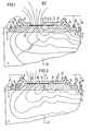
- FIGS. 1 to 4 show cross sections through a part of the semi-le iter emotions and the electrodes of four different embodiments. The same parts are provided with the same reference numerals.
- the substrate of the semiconductor body is designated by 1.
- a zone 2 with the conductivity type opposite to the substrate is planarly embedded in the substrate.
- Zone 2 and substrate 1 adjoin one another at a pn junction 3.
- the surface of the semiconductor body is provided with an insulating layer 4, which usually consists of silicon dioxide Si0 2 . It covers the pn junction 3 where it touches the surface of the semi-lead ter stressess occurs and extends to close to the edge 5 of the semiconductor body.
- a channel stopper 6 is provided, which sits on the insulating layer 4. The channel stopper is electrically connected to the substrate 1.
- the steps of the channel stopper can be made from a single layer of doped poly Silicon exist. Other conductive materials are also possible.
- the channel stopper 6 can also consist of more than two stages; the third stage then has a greater distance from the surface 20 of the semiconductor body than the stage 8.
- the third stage consists of a metal electrode 9 which overlaps the second stage 8.
- the metal electrode 9 is also contacted with the substrate and thus forms part of the channel stopper 6.
- the field plate 10 is electrically connected to the zone 2 via an electrode 14.
- the pn junction 3 When a voltage with the indicated polarity is applied, the pn junction 3 is biased in the reverse direction. A space-charge-free zone is thus formed, the equipotential lines of which are designated by 17. Due to the increasing distance of the channel stopper from the surface 20 towards zone 2, the equipotential lines 17 running under the channel stopper have a large radius of curvature. This means that the field strength inside the semiconductor body is kept small. It is also achieved that the equipotential lines pass through the surface 20 of the semiconductor body at a large distance from one another. That means that Surface field strength can be kept low. By suitable dimensioning it is possible to closely approximate the surface opening to the opening inside the semiconductor body.
- the course of the equipotential lines between zone 2 and the channel stopper can be further improved by the above-mentioned field plate 10 and by an auxiliary electrode 15.
- the auxiliary electrode 15 has an in. Direction to the edge 5 of the semiconductor body increasing distance and overlaps the zone 2 with its part closest to the surface 20. It is contacted by an electrode 16 with the electrode 14 and the field plate 10.
- the field plate 10 can consist of several parts and have a strip or ring-shaped electrode 11 which is electrically connected to the field plate 10 by a web 12.
- the electrode 11 influences the shape of the equipotential lines in such a way that small radii of curvature are avoided even in the area under the field plate.
- the equipotential lines 17 then emerge through the surface of the insulating layer 4.
- passivation layers 13 are provided which, for. B. can consist of evaporated, amorphous silicon.
- a reverse voltage of 1000 V was achieved with such a semiconductor component, compared to a semiconductor component with a simple channel stopper, which only reached a reverse voltage of 700 V.
- the semiconductor component according to FIG. 2 differs from that according to FIG. 1 in that several field-shaped electrodes 11 and 18 are assigned to the field plate 10.
- the electrodes 11 and 18 are connected to the field plate 10 by webs 13 and 19, respectively.
- the course of the equipotential lines under the electrodes 11 and 18 and under the field plate 10 is particularly favorable when the electrode 11 is at a smaller distance from the field plate 10 than the electrode 18 from the electrode 11.
- the distance between 11 and 18 can be between 20 and 50 / um and the distance between 11 and 10 are between 10 and 25 ⁇ m. All other sizes can be selected in accordance with the exemplary embodiment according to FIG. 1.
- FIG. 3 Particularly stable characteristic curves are obtained with a semiconductor component according to FIG. 3, whose insulating layer 4 is almost completely covered, or with a semiconductor component according to FIG. 4, whose insulating layer 4 is completely covered by the field plate.
- the top stage 9 of the channel stopper is connected to the field plate 21 by a web 22.
- This embodiment is for smaller blocking voltages are suitable since the equipotential lines in the space 23 between the field plate and the upper stage 8 of the channel stopper 6 are pressed together.
- the material of the insulating layer 4 e.g. B. silicon dioxide, has a much higher breakdown voltage than silicon, but the relatively small distance between the field plate and channel stopper limits the applicability to 200 to 300 V reverse voltage.
- a passivation layer 13 which can likewise consist of evaporated silicon.
- Very stable characteristics are obtained with the embodiment example according to FIG. 4, in which the field plate 24 overlaps the channel stopper 6.
- the field lines in the space 23 between the field plate 24 and the channel stopper 6 are pushed together, so that this embodiment is also limited to reverse voltages between 200 and 300 V.
- the invention is applicable to all planar semiconductor components, e.g. B. thyristors, bipolar transistors, MOS transistors and diodes are suitable.
- the channel stopper is arranged around this system on the edge of the semiconductor body.
- the channel stopper is located between the edge of the semiconductor chip and the systems adjacent to the edge.
Landscapes
- Electrodes Of Semiconductors (AREA)
- Bipolar Transistors (AREA)
- Element Separation (AREA)
- Metal-Oxide And Bipolar Metal-Oxide Semiconductor Integrated Circuits (AREA)
- Hall/Mr Elements (AREA)
Abstract
Description
- Die Erfindung bezieht sich auf ein Halbleiterbauelement mit einem Halbleiterkörper, bestehend aus einem Substrat vom ersten Leitungstyp und mindestens einer im Substrat planar eingebetteten Zone entgegengesetzten Leitungstyps, mit einer Isolierschicht auf derjenigen Oberfläche, an der die eingebettete Zone liegt, mit einer diese Zone kontaktierenden Elektrode, mit einem außerhalb dieser Zone am Rand des Halbleiterkörpers auf der Isolierschicht angeordneten Channel-Stopper, der elektrisch mit dem Substrat verbunden ist, und mit einer auf der Isolierschicht angeordneten, zwischen dieser Zöne und dem Channel-Stopper liegenden Feldplatte, die elektrisch mit der Zone verbunden ist.
- Ein solches Halbleiterbauelement ist z. B. in den "Siemens Forschungs- und Entwicklungs-Berichten", Band 9 (1980), Nr. 4, Seite 186 beschrieben worden. In Fig. 13 dieser Veröffentlichung ist ein MOS-Leistungstransistor mit den eingangs erwähnten Merkmalen gezeigt. Der am Rand des Transistors liegende Channel-Stopper verhindert eine Ausweitung der Raumladungszone bis an den Rand des Substrats. Die Äquipotentiallinien treten dann ausschließlich zwischen Channel-Stopper und Feldplatte durch die Oberfläche des Halbleiterkörpers. Der Channel-Stopper besteht aus einer Aluminiumleiterbahn, die mit dem Substrat kontaktiert ist und die die Isolierschicht ein Stück überlappt. Es hat-sich gezeigt, daß ein solcher einfacher Channel-Stopper eine scharfe Krümmung der Äquipotentiallinien im Oberflächenbereich des Halbleiterkörpers verursacht. Dies bringt eine hohe Feldstärke im Oberflächenbereich des Halbleiterkörpers mit sich, was zum Oberflächendurchbruch führen kann. Die Durch- bruchsspannung an der Oberfläche ist dabei wesentlich geringer als im Halbleiterkörper selbst. Dieses Problem tritt nicht nur bei einem MOS-Leistungstransistor auf, sondern bei allen planaren Halbleiterbauelementen.
- Der Erfindung liegt die Aufgabe zugrunde, ein Halbleiterbauelement der eingangs erwähnten Art so weiterzubilden, daß die starke Krümmung der Äquipotentiallinien im Oberflächenbereich des Halbleiterkörpers vermieden wird.
- Diese Aufgabe wird dadurch gelöst, daß der Channel-Stopper in zunehmender Entfernung vom Rand des Halbleiterkörpers in Richtung zur genannten Zone einen zunehmenden Abstand zur Oberfläche des Halbleiterkörpers aufweist.
- Weiterbildungen der Erfindung sind Gegenstand der Unteransprüche.
- Die Erfindung wird an Hand einiger Ausführungsbeispiele in Verbindung mit den Fig. 1 bis 4 näher erläutert. Die Figuren zeigen Querschnitte durch einen Teil der Halb- leiterkörper und die Elektroden von vier verschiedenen Ausführungsbeispielen. Gleiche Teile sind mit gleichen Bezugszeichen versehen.
- In Fig. 1 ist das Substrat des Halbleiterkörpers mit 1 bezeichnet. In das Substrat ist eine Zone 2 mit dem Substrat entgegengesetzten Leitungstyp planar eingebettet. Die Zone 2 und das Substrat 1 grenzen an einem pn-Übergang 3 aneinander. Die Oberfläche des Halbleiterkörpers ist mit einer Isolierschicht 4 versehen, die üblicherweise aus Siliciumdioxid Si02 besteht. Sie überdeckt den pn-Übergang 3 dort, wo er an die Oberfläche des Halbleiterkörpers tritt und erstreckt sich bis nahe an den Rand 5 des Halbleiterkörpers. Am Rand 5 ist ein Channel-Stopper 6 vorgesehen, der auf der Isolierschicht 4 sitzt. Der Channel-Stopper ist elektrisch mit dem Substrat 1 verbunden. Er besteht aus zwei Stufen 7 und 8, wobei die weiter vom Rand 5 entfernte Stufe 8 einen größeren Abstand von der Oberfläche 20 des Halbleiterkörpers hat als die dem Rand benachbarte Stufe 7. Die Stufen des Channel-Stoppers können aus einer einzigen Schicht dotierten Poly-Siliciums bestehen. Andere leitende Materialien sind ebenfalls möglich.
- Der Channel-Stopper 6 kann auch aus mehr als zwei Stufen bestehen; die dritte Stufe hat dann wiederum einen gröBeren Abstand von der Oberfläche 20 des Halbleiterkörpers als die Stufe 8. Im Ausführungsbeispiel nach Fig. 1 besteht die dritte Stufe aus einer Metallelektrode 9, die die zweite Stufe 8 überlappt. Die Metallelektrode 9 ist ebenfalls mit dem Substrat kontaktiert und bildet damit einen Teil des Channel-Stoppers 6. Auf der Isolierschicht 4 sitzt noch eine Feldplatte 10, deren Zweck weiter unten erläutert wird. Die Feldplatte 10 ist über eine Elektrode 14 mit der Zone 2 elektrisch verbunden.
- Bei Anlegen einer Spannung mit der eingezeichneten Polarität wird der pn-Übergang 3 in Sperrichtung vorgespannt. Damit bildet sich eine raumladungsfreie Zone aus, deren Äquipotentiallinien mit 17 bezeichnet sind. Bedingt durch den zur Zone 2 hin zunehmenden Abstand des Channel-Stoppers von der Oberfläche 20 weisen die unter dem Channel-Stopper verlaufenden Äquipotentiallinien 17 einen großen Krümmungsradius auf. Das heißt, daß die Feldstärke im Innern des Halbleiterkörpers klein gehalten wird. Außerdem wird erreicht, daß die Äquipotentiallinien in weitem Abstand voneinander durch die Oberfläche 20 des Halbleiterkörpers treten. Das heißt, daß die Oberflächenfeldstärke gering gehalten werden kann. Durch geeignete Dimensionierung ist es möglich, den Oberflächendurchbruch dem Durchbruch im Innern des Halbleiterkörpers stark anzunähern.
- Der Verlauf der Äquipotentiallinien zwischen der Zone 2 und dem Channel-Stopper kann durch die oben erwähnte Feldplatte 10 und durch eine Hilfselektrode 15 weiter verbessert werden. Die Hilfselektrode 15 weist einen in . Richtung zum Rand 5 des Halbleiterkörpers zunehmenden Abstand auf und überlappt die Zone 2 mit ihrem der Oberfläche 20 am nächsten liegenden Teil. Sie ist durch eine Elektrode 16 mit der Elektrode 14 und der Feldplatte 10 kontaktiert. Die Feldplatte 10 kann aus mehreren Teilen bestehen und eine streifen- oder ringförmige Elektrode 11 aufweisen, die mit der Feldplatte 10 durch einen Steg 12 elektrisch verbunden ist. Die Elektrode 11 beeinflußt dabei die Form der Äquipotentiallinien derart, daß auch im Bereich unter der Feldplatte kleine Krümmungsradien vermieden werden. Die Äquipotentiallinien 17 treten dann durch die Oberfläche der Isolierschicht 4 aus. Zur Passivierung der von Elektroden nicht bedeckten Oberflächenteile der Isolierschicht 4 sind Passivierungsschichten 13 vorgesehen, die z. B. aus aufgedampftem, amorphem Silicium bestehen können.
- Das in Fig. 1 gezeigte Ausführungsbeispiel kann etwa die folgenden Abmessungen haben: Abstand der Stufe 7 von der Oberfläche des Halbleiterkörpers 20 = 0,1 µm; Abstand der Stufe 8 von der Oberfläche = 0,5 bis 1 µm; Mindestabstand der Elektrode 9 von der Oberfläche = 1 bis 2 µm; Abstand der Elektrode 9 von der streifenförmigen Elektrode 11 = 3 bis 15 µm; Breite der Elektrode 11 = 5 bis 10 µm; Abstand Elektrode 11 - Feldplatte 10 = 20 bis 50 /um je nach Sperrspannung; Abstand der Hilfselektrode 15 entsprechend dem Channel-Stopper 6; Dotierung der Zone 2 = 1018 bis 1020 cm-3; Dotierung des Substrats 1 = 2. 10 14 cm-3.
- Mit einem solchen Halbleiterbauelement wurde eine Sperrspannung von 1000 V erreicht, gegenüber einem Halbleiterbauelement mit einem einfachen Channel-Stopper, das lediglich eine Sperrspannung von 700 V erreichte.
- Das Halbleiterbauelement nach Fig. 2 unterscheidet sich von dem nach Fig. 1 dadurch,.daß der Feldplatte 10 mehrere streifenförmige Elektroden 11 und 18 zugeordnet sind. Die Elektroden 11 und 18 sind durch Stege 13 bzw. 19 mit der Feldplatte 10 verbunden. Auch hier ergeben sich große Krümmungsradien und große Abstände der Äquipotentiallinien beim Durchtritt durch die Oberfläche 20 des Halbleiterkörpers. Besonders günstig wird der Verlauf der Äquipotentiallinien unter den Elektroden 11 und 18 sowie unter der Feldplatte 10 dann, wenn die Elektrode 11 einen kleineren Abstand von der Feldplatte 10 hat als die Elektrode 18 von der Elektrode 11. Der Abstand zwischen 11 und 18 kann dabei zwischen 20 und 50 /um und der Abstand zwischen 11 und 10 zwischen 10 und 25 µm liegen. Alle anderen Größen können entsprechend dem AusfUhrungsbeispiel nach Fig. 1 gewählt werden.
- Besonders stabile Kennlinien erhält man bei einem Halbleiterbauelement nach Fig. 3, dessen Isolierschicht 4 fast vollständig bedeckt ist oder bei einem Halbleiterbauelement nach Fig. 4, dessen Isolierschicht 4 vollständig von der Feldplatte bedeckt ist. Beim Bauelement nach Fig. 3 ist die oberste Stufe 9 des Channel-Stoppers durch einen Steg 22 mit der Feldplatte 21 verbunden. Es liegen nur noch die Stufen 7 und 8 des Channel-Stoppers 6 auf Substratpotential. Diese Ausführungsform ist für kleinere Sperrspannungen geeignet, da die Äquipotentiallinien im Zwischenraum 23 zwischen der Feldplatte und der oberen Stufe 8 des Channel-Stoppers 6 zusammengedrängt werden. Das Material der Isolierschicht 4, z. B. Siliciumdioxid, hat zwar eine wesentlich höhere Durchbruchsspannung als Silicium, der relativ geringe Abstand zwischen Feldplatte und Channel-Stopper begrenzt die Anwendbarkeit jedoch auf 200 bis 300 V Sperrspannung. Die von der Feldplatte 21 nicht bedeckten Oberflächenteile der Isolierschicht 4 sind wieder von einer Passivierungsschicht 13 bedeckt, die ebenfalls aus aufgedampftem Silicium bestehen kann. Sehr stabile Kennlinien werden mit dem Ausführungs beispiel nach Fig. 4 erhalten, bei dem die Feldplatte 24 den Channel-Stopper 6 überlappt. Auch hier werden die Feldlinien im Zwischenraum 23 zwischen Feldplatte 24 und Channel-Stopper 6 zusammengedrängt, so daß diese Ausführungsform ebenfalls auf Sperrspannungen zwischen 200 und 300 V beschränkt bleibt.
- Die Erfindung ist für alle planaren Halbleiterbauelemente, z. B. Thyristoren, Bipolartransistoren, MOS-Transistoren und Dioden geeignet. Bei Halbleiterbauelementen mit nur einem einzigen System auf einem Halbleiterchip ist der Channel-Stopper rings um dieses System am Rand des Halbleiterkörpers herum angeordnet. Bei Halblei-terchips mit mehreren Systemen, wie dies z. B. bei Leistungs-MOS-Transistoren und -Thyristoren der Fall ist, liegt der Channel-Stopper jeweils zwischen dem Rand-des Halbleiterchips und den dem Rand benachbarten Systemen.
Claims (9)
Applications Claiming Priority (2)
| Application Number | Priority Date | Filing Date | Title |
|---|---|---|---|
| DE3141203 | 1981-10-16 | ||
| DE19813141203 DE3141203A1 (de) | 1981-10-16 | 1981-10-16 | Planares halbleiterbauelement |
Publications (3)
| Publication Number | Publication Date |
|---|---|
| EP0077481A2 true EP0077481A2 (de) | 1983-04-27 |
| EP0077481A3 EP0077481A3 (en) | 1984-07-25 |
| EP0077481B1 EP0077481B1 (de) | 1987-12-23 |
Family
ID=6144287
Family Applications (1)
| Application Number | Title | Priority Date | Filing Date |
|---|---|---|---|
| EP82109015A Expired EP0077481B1 (de) | 1981-10-16 | 1982-09-29 | Planares Halbleiterbauelement |
Country Status (4)
| Country | Link |
|---|---|
| US (1) | US5311052A (de) |
| EP (1) | EP0077481B1 (de) |
| JP (1) | JPH065692B2 (de) |
| DE (2) | DE3141203A1 (de) |
Cited By (4)
| Publication number | Priority date | Publication date | Assignee | Title |
|---|---|---|---|---|
| EP0660416A1 (de) * | 1993-12-22 | 1995-06-28 | AT&T Corp. | Halbleiteranordnung mit vermindertem Randabschluss und hoher Durchbruchspannung |
| DE4024728B4 (de) * | 1989-08-03 | 2004-09-30 | Fuji Electric Co., Ltd., Kawasaki | MOS-Halbleitereinrichtung und Verfahren zu ihrer Herstellung |
| DE10358985B3 (de) * | 2003-12-16 | 2005-05-19 | Infineon Technologies Ag | Halbleiterbauelement mit einem pn-Übergang und einer auf einer Oberfläche aufgebrachten Passivierungsschicht |
| DE4042699B4 (de) * | 1989-08-03 | 2007-04-12 | Fuji Electric Co., Ltd., Kawasaki | MOS-Halbleitereinrichtung |
Families Citing this family (12)
| Publication number | Priority date | Publication date | Assignee | Title |
|---|---|---|---|---|
| DE58905356D1 (de) * | 1988-05-11 | 1993-09-30 | Siemens Ag | MOS-Halbleiterbauelement für hohe Sperrspannung. |
| DE59010855D1 (de) * | 1990-06-05 | 1998-12-24 | Siemens Ag | Herstellverfahren für einen Leistungs-MISFET |
| EP0485648B1 (de) * | 1990-11-12 | 1995-05-24 | Siemens Aktiengesellschaft | Halbleiterbauelement für hohe Sperrspannung |
| KR0175277B1 (ko) | 1996-02-29 | 1999-02-01 | 김광호 | 중첩된 필드플레이트구조를 갖는 전력반도체장치 및 그의 제조방법 |
| DE19741167C2 (de) * | 1997-09-18 | 1999-08-12 | Siemens Ag | Randstruktur für ein Halbleiterbauelement |
| US5918137A (en) * | 1998-04-27 | 1999-06-29 | Spectrian, Inc. | MOS transistor with shield coplanar with gate electrode |
| DE19839971C2 (de) * | 1998-09-02 | 2000-11-30 | Siemens Ag | Randstruktur für Halbleiterbauelemente |
| JP3776666B2 (ja) | 2000-02-25 | 2006-05-17 | 沖電気工業株式会社 | 半導体装置 |
| DE102004037153B4 (de) * | 2004-07-30 | 2011-09-15 | Infineon Technologies Ag | Verfahren zum Herstellen eines Leistungshalbleiterbauteils |
| DE102007030755B3 (de) * | 2007-07-02 | 2009-02-19 | Infineon Technologies Austria Ag | Halbleiterbauelement mit einem einen Graben aufweisenden Randabschluss und Verfahren zur Herstellung eines Randabschlusses |
| JP5843801B2 (ja) | 2013-03-19 | 2016-01-13 | 株式会社東芝 | 情報処理装置およびデバッグ方法 |
| JP6101183B2 (ja) | 2013-06-20 | 2017-03-22 | 株式会社東芝 | 半導体装置 |
Family Cites Families (12)
| Publication number | Priority date | Publication date | Assignee | Title |
|---|---|---|---|---|
| NL6413894A (de) * | 1964-02-04 | 1965-08-05 | ||
| US3602782A (en) * | 1969-12-05 | 1971-08-31 | Thomas Klein | Conductor-insulator-semiconductor fieldeffect transistor with semiconductor layer embedded in dielectric underneath interconnection layer |
| US3767981A (en) * | 1971-06-04 | 1973-10-23 | Signetics Corp | High voltage planar diode structure and method |
| DE2241600A1 (de) * | 1971-08-26 | 1973-03-01 | Dionics Inc | Hochspannungs-p-n-uebergang und seine anwendung in halbleiterschaltelementen, sowie verfahren zu seiner herstellung |
| US3906539A (en) * | 1971-09-22 | 1975-09-16 | Philips Corp | Capacitance diode having a large capacitance ratio |
| JPS573225B2 (de) * | 1974-08-19 | 1982-01-20 | ||
| JPS54388A (en) * | 1977-05-31 | 1979-01-05 | Chikashi Uemura | Connecting device for float ship |
| NL169711C (nl) * | 1977-06-01 | 1982-08-16 | Ihc Holland Nv | Inrichting voor het constant houden van de trekspanning in een kabel. |
| US4134125A (en) * | 1977-07-20 | 1979-01-09 | Bell Telephone Laboratories, Incorporated | Passivation of metallized semiconductor substrates |
| JPS5552272A (en) * | 1978-10-13 | 1980-04-16 | Seiko Epson Corp | High withstanding voltage dsa mos transistor |
| DE3046749C2 (de) * | 1979-12-10 | 1986-01-16 | Sharp K.K., Osaka | MOS-Transistor für hohe Betriebsspannungen |
| DE3012430A1 (de) * | 1980-03-31 | 1981-10-08 | Siemens AG, 1000 Berlin und 8000 München | Planare halbleiteranordnung mit erhoehter durchbruchsspannung |
-
1981
- 1981-10-16 DE DE19813141203 patent/DE3141203A1/de not_active Withdrawn
-
1982
- 1982-09-29 DE DE8282109015T patent/DE3277891D1/de not_active Expired
- 1982-09-29 EP EP82109015A patent/EP0077481B1/de not_active Expired
- 1982-09-29 US US06/426,783 patent/US5311052A/en not_active Expired - Lifetime
- 1982-10-13 JP JP57179672A patent/JPH065692B2/ja not_active Expired - Lifetime
Cited By (5)
| Publication number | Priority date | Publication date | Assignee | Title |
|---|---|---|---|---|
| DE4024728B4 (de) * | 1989-08-03 | 2004-09-30 | Fuji Electric Co., Ltd., Kawasaki | MOS-Halbleitereinrichtung und Verfahren zu ihrer Herstellung |
| DE4042699B4 (de) * | 1989-08-03 | 2007-04-12 | Fuji Electric Co., Ltd., Kawasaki | MOS-Halbleitereinrichtung |
| EP0660416A1 (de) * | 1993-12-22 | 1995-06-28 | AT&T Corp. | Halbleiteranordnung mit vermindertem Randabschluss und hoher Durchbruchspannung |
| DE10358985B3 (de) * | 2003-12-16 | 2005-05-19 | Infineon Technologies Ag | Halbleiterbauelement mit einem pn-Übergang und einer auf einer Oberfläche aufgebrachten Passivierungsschicht |
| US7187058B2 (en) | 2003-12-16 | 2007-03-06 | Infineon Technologies Ag | Semiconductor component having a pn junction and a passivation layer applied on a surface |
Also Published As
| Publication number | Publication date |
|---|---|
| EP0077481B1 (de) | 1987-12-23 |
| DE3141203A1 (de) | 1983-04-28 |
| US5311052A (en) | 1994-05-10 |
| EP0077481A3 (en) | 1984-07-25 |
| JPS5877242A (ja) | 1983-05-10 |
| DE3277891D1 (en) | 1988-02-04 |
| JPH065692B2 (ja) | 1994-01-19 |
Similar Documents
| Publication | Publication Date | Title |
|---|---|---|
| DE19854915C2 (de) | MOS-Feldeffekttransistor mit Hilfselektrode | |
| EP0077481B1 (de) | Planares Halbleiterbauelement | |
| DE19811297B4 (de) | MOS-Halbleitervorrichtung mit hoher Durchbruchspannung | |
| DE2706623C2 (de) | ||
| EP0095755B1 (de) | Halbleiterbauelement mit Planarstruktur | |
| EP0888639A1 (de) | Durch feldeffekt steuerbares halbleiterbauelement | |
| EP0011879B1 (de) | Feldeffekttransistor | |
| DE69937101T2 (de) | Laterale-dünnfilm-silizium-auf-isolator (soi) anordnung mit mehreren gebieten im drift-gebiet | |
| DE4309764A1 (de) | Leistungs-MOSFET | |
| EP0057256A2 (de) | Vertikal-MIS-Feldeffekttransistor mit kleinem Durchlasswiderstand | |
| DE3040775C2 (de) | Steuerbares MIS-Halbleiterbauelement | |
| EP0037115B1 (de) | Planare Halbleiteranordnung mit erhöhter Durchbruchsspannung | |
| EP0014435B1 (de) | Thyristor mit Steuerung durch Feldeffekttransistor | |
| DE19604044C2 (de) | Durch Feldeffekt steuerbares Halbleiterbauelement | |
| EP0098496A1 (de) | IGFET mit Injektorzone | |
| DE10252609B4 (de) | Abschluß für ein Halbleiterbauteil mit MOS-Gatesteuerung mit Schutzringen | |
| DE10057612A1 (de) | Vertikales Halbleiterbauelement mit vertikalem Randabschluss | |
| DE3114971A1 (de) | Dmos-halbleiterbauelement | |
| WO1999059208A1 (de) | Hochspannungs-halbleiter-bauelement und verfahren zu seiner herstellung sowie verwendung des halbleiter-bauelements | |
| EP0834926A2 (de) | Durch Feldeffekt steuerbares Halbleiterbauelement | |
| DE3200660A1 (de) | Mis-feldeffekttransistor mit ladungstraegerinjektion | |
| DE19839971C2 (de) | Randstruktur für Halbleiterbauelemente | |
| DE3044341A1 (de) | Fototransistor | |
| DE19923520C1 (de) | Randstruktur für Halbleiterbauelemente | |
| EP1320896B1 (de) | Körper aus halbleitermaterial mit reduzierter mittlerer freier weglänge |
Legal Events
| Date | Code | Title | Description |
|---|---|---|---|
| PUAI | Public reference made under article 153(3) epc to a published international application that has entered the european phase |
Free format text: ORIGINAL CODE: 0009012 |
|
| AK | Designated contracting states |
Designated state(s): CH DE FR GB IT LI |
|
| PUAL | Search report despatched |
Free format text: ORIGINAL CODE: 0009013 |
|
| AK | Designated contracting states |
Designated state(s): CH DE FR GB IT LI |
|
| 17P | Request for examination filed |
Effective date: 19840824 |
|
| GRAA | (expected) grant |
Free format text: ORIGINAL CODE: 0009210 |
|
| AK | Designated contracting states |
Kind code of ref document: B1 Designated state(s): CH DE FR GB IT LI |
|
| REF | Corresponds to: |
Ref document number: 3277891 Country of ref document: DE Date of ref document: 19880204 |
|
| ET | Fr: translation filed | ||
| ITF | It: translation for a ep patent filed | ||
| GBT | Gb: translation of ep patent filed (gb section 77(6)(a)/1977) | ||
| PLBE | No opposition filed within time limit |
Free format text: ORIGINAL CODE: 0009261 |
|
| STAA | Information on the status of an ep patent application or granted ep patent |
Free format text: STATUS: NO OPPOSITION FILED WITHIN TIME LIMIT |
|
| 26N | No opposition filed | ||
| PGFP | Annual fee paid to national office [announced via postgrant information from national office to epo] |
Ref country code: CH Payment date: 19891218 Year of fee payment: 8 |
|
| PG25 | Lapsed in a contracting state [announced via postgrant information from national office to epo] |
Ref country code: LI Effective date: 19900930 Ref country code: CH Effective date: 19900930 |
|
| REG | Reference to a national code |
Ref country code: CH Ref legal event code: PL |
|
| ITTA | It: last paid annual fee | ||
| PGFP | Annual fee paid to national office [announced via postgrant information from national office to epo] |
Ref country code: GB Payment date: 19980817 Year of fee payment: 17 |
|
| PGFP | Annual fee paid to national office [announced via postgrant information from national office to epo] |
Ref country code: FR Payment date: 19980916 Year of fee payment: 17 |
|
| PG25 | Lapsed in a contracting state [announced via postgrant information from national office to epo] |
Ref country code: GB Free format text: LAPSE BECAUSE OF NON-PAYMENT OF DUE FEES Effective date: 19990929 |
|
| GBPC | Gb: european patent ceased through non-payment of renewal fee |
Effective date: 19990929 |
|
| PG25 | Lapsed in a contracting state [announced via postgrant information from national office to epo] |
Ref country code: FR Free format text: LAPSE BECAUSE OF NON-PAYMENT OF DUE FEES Effective date: 20000531 |
|
| REG | Reference to a national code |
Ref country code: FR Ref legal event code: ST |
|
| PGFP | Annual fee paid to national office [announced via postgrant information from national office to epo] |
Ref country code: DE Payment date: 20011119 Year of fee payment: 20 |