EP0077535B1 - Verfahren zum Herstellen von Schichten aus hochschmelzenden Metallen bei niedrigen Substrattemperaturen - Google Patents
Verfahren zum Herstellen von Schichten aus hochschmelzenden Metallen bei niedrigen Substrattemperaturen Download PDFInfo
- Publication number
- EP0077535B1 EP0077535B1 EP82109524A EP82109524A EP0077535B1 EP 0077535 B1 EP0077535 B1 EP 0077535B1 EP 82109524 A EP82109524 A EP 82109524A EP 82109524 A EP82109524 A EP 82109524A EP 0077535 B1 EP0077535 B1 EP 0077535B1
- Authority
- EP
- European Patent Office
- Prior art keywords
- production
- silane
- compounds
- sih
- tantalum
- Prior art date
- Legal status (The legal status is an assumption and is not a legal conclusion. Google has not performed a legal analysis and makes no representation as to the accuracy of the status listed.)
- Expired
Links
Images
Classifications
-
- C—CHEMISTRY; METALLURGY
- C23—COATING METALLIC MATERIAL; COATING MATERIAL WITH METALLIC MATERIAL; CHEMICAL SURFACE TREATMENT; DIFFUSION TREATMENT OF METALLIC MATERIAL; COATING BY VACUUM EVAPORATION, BY SPUTTERING, BY ION IMPLANTATION OR BY CHEMICAL VAPOUR DEPOSITION, IN GENERAL; INHIBITING CORROSION OF METALLIC MATERIAL OR INCRUSTATION IN GENERAL
- C23C—COATING METALLIC MATERIAL; COATING MATERIAL WITH METALLIC MATERIAL; SURFACE TREATMENT OF METALLIC MATERIAL BY DIFFUSION INTO THE SURFACE, BY CHEMICAL CONVERSION OR SUBSTITUTION; COATING BY VACUUM EVAPORATION, BY SPUTTERING, BY ION IMPLANTATION OR BY CHEMICAL VAPOUR DEPOSITION, IN GENERAL
- C23C16/00—Chemical coating by decomposition of gaseous compounds, without leaving reaction products of surface material in the coating, i.e. chemical vapour deposition [CVD] processes
-
- C—CHEMISTRY; METALLURGY
- C23—COATING METALLIC MATERIAL; COATING MATERIAL WITH METALLIC MATERIAL; CHEMICAL SURFACE TREATMENT; DIFFUSION TREATMENT OF METALLIC MATERIAL; COATING BY VACUUM EVAPORATION, BY SPUTTERING, BY ION IMPLANTATION OR BY CHEMICAL VAPOUR DEPOSITION, IN GENERAL; INHIBITING CORROSION OF METALLIC MATERIAL OR INCRUSTATION IN GENERAL
- C23C—COATING METALLIC MATERIAL; COATING MATERIAL WITH METALLIC MATERIAL; SURFACE TREATMENT OF METALLIC MATERIAL BY DIFFUSION INTO THE SURFACE, BY CHEMICAL CONVERSION OR SUBSTITUTION; COATING BY VACUUM EVAPORATION, BY SPUTTERING, BY ION IMPLANTATION OR BY CHEMICAL VAPOUR DEPOSITION, IN GENERAL
- C23C16/00—Chemical coating by decomposition of gaseous compounds, without leaving reaction products of surface material in the coating, i.e. chemical vapour deposition [CVD] processes
- C23C16/06—Chemical coating by decomposition of gaseous compounds, without leaving reaction products of surface material in the coating, i.e. chemical vapour deposition [CVD] processes characterised by the deposition of metallic material
- C23C16/08—Chemical coating by decomposition of gaseous compounds, without leaving reaction products of surface material in the coating, i.e. chemical vapour deposition [CVD] processes characterised by the deposition of metallic material from metal halides
-
- H—ELECTRICITY
- H10—SEMICONDUCTOR DEVICES; ELECTRIC SOLID-STATE DEVICES NOT OTHERWISE PROVIDED FOR
- H10P—GENERIC PROCESSES OR APPARATUS FOR THE MANUFACTURE OR TREATMENT OF DEVICES COVERED BY CLASS H10
- H10P14/00—Formation of materials, e.g. in the shape of layers or pillars
- H10P14/40—Formation of materials, e.g. in the shape of layers or pillars of conductive or resistive materials
- H10P14/412—Deposition of metallic or metal-silicide materials
-
- H—ELECTRICITY
- H10—SEMICONDUCTOR DEVICES; ELECTRIC SOLID-STATE DEVICES NOT OTHERWISE PROVIDED FOR
- H10P—GENERIC PROCESSES OR APPARATUS FOR THE MANUFACTURE OR TREATMENT OF DEVICES COVERED BY CLASS H10
- H10P14/00—Formation of materials, e.g. in the shape of layers or pillars
- H10P14/40—Formation of materials, e.g. in the shape of layers or pillars of conductive or resistive materials
- H10P14/42—Formation of materials, e.g. in the shape of layers or pillars of conductive or resistive materials using a gas or vapour
- H10P14/43—Chemical deposition, e.g. chemical vapour deposition [CVD]
Definitions
- the present patent application relates to a method for producing layers consisting of tantalum, tungsten or molybdenum on substrates at low substrate temperatures, the starting materials used being the halides of these metals which are thermally decomposed and reduced in the gas phase in the presence of silane (SiH 4 ) .
- metallic layers are used as resistors, electrodes for capacitors and as inductors, on structured semiconductor crystal wafers as conductor tracks.
- metal coatings are also used to protect against corrosion and wear on workpieces with complex shapes.
- a wide variety of methods are used to produce such layers, such as galvanic deposition, vapor deposition, ion plating or dusting.
- a common feature of all methods of layer production is that the material is deposited at low temperatures and in the presence of foreign atoms compared to its melting point. Low temperatures are possible, for example, with galvanic deposition.
- this type of deposition cannot be carried out with high-melting metals such as tantalum, tungsten and molybdenum, since these metals cannot be separated by electroplating.
- Edge coverage is important for the production of layers on structured semiconductor crystal wafers.
- CVD chemical vapor disposition
- Modified CVD processes are therefore proposed for such coatings, in which the reaction temperatures are reduced either by using organometallic starting compounds or by using a high-frequency plasma as an energy source.
- organometallic starting compounds See Zeitschrift. Kni Kunststofftechnik / J. Of Materials Technology, 4th year, 1973, No. 7, pp. 379 to 386
- metals and their compounds such as oxides, nitrides and carbides can be produced, however due to the organic component, impurities are incorporated in the coating.
- a method for CVD deposition of refractory metals can be found in DE-OS 2445564.
- the reaction temperature is above 600 ° C.
- the object on which the invention is based consists in the production of high-melting pure metal layers made of tantalum, tungsten or molybdenum, as are used in particular for multilayer wiring on structured semiconductor crystal wafers. Due to the good edge coverage, a CVD process (precipitation due to thermal decomposition and reduction) should be applicable at low reaction temperatures.
- halides of these metals are thermally decomposed and reduced in the presence of silane (SiH 4 ) at temperatures ⁇ 500 ° C. and in the pressure range from 25 Pa to 11 ⁇ 10 3 Pa from the gas phase.
- SiH 4 silane
- AB halide of tantalum, tungsten, molybdenum
- CD silane
- CB silicon halide
- D hydrogen. It is essential that the temperature for the thermal decomposition or reduction of the individual components (AB, CD) is higher than for the mixture (AB + CD).
- the gaseous starting compounds are passed through the heating zone of a reactor, decomposed there, the metals are deposited on the substrates and the resulting gaseous decomposition products are carried away from the reaction zone, with additional carrier gases being used to maintain and support a laminar flow in the reaction space consisting of hydrogen and / or noble gases can be used.
- additional carrier gases being used to maintain and support a laminar flow in the reaction space consisting of hydrogen and / or noble gases can be used.
- the derivation of the decomposition products is of great importance for the layer purity.
- very pure and very homogeneous in terms of their layer thickness starting from tungsten hexafluoride (WF 6 ) and silane (SiH 4 ), are produced already at 150 ° C. (generally at temperatures from 120 to 200 ° C.) posed.
- WF 6 tungsten hexafluoride
- SiH 4 silane
- tantalum chloride (TaC1 5 ) and molybdenum chloride (MoC1 5 ) can be used to produce metal layers from tantalum and molybdenum.
- the metal layers according to the invention are characterized by good edge coverage and high thermal stability. When coating workpieces, they are comparable in terms of corrosion and wear protection to workpieces made of expensive and high-temperature-resistant base materials.
- the metal layers can be deposited in all commercial CVD apparatus.
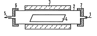
- the starting compounds consisting of tungsten hexafluoride and silane (AB, CD) are introduced into the gas composition two volumes of tungsten hexafluoride and three volumes of silane at the gas inlet indicated by arrow 1 into the quartz reactor tube 2 and in the region of the tube furnace 3 at 150 ° C held heating zone at a pressure of 60 Pa to 1.3 ⁇ 10 3 Pa according to the reaction decomposes. This results in a growth rate of tungsten of 5 to 15 ⁇ m / h on the substrates 4 located in the heating zone.
- the decomposition products consisting of hydrogen and silicon tetrafluoride leave the reaction space (2) at the gas outlet indicated by arrow 5, to which the pump for adjusting the pressure is also connected.
- the brackets supporting the quartz tube 2 are designated by the reference numerals 6 and 7.
- Tantalum and molybdenum layers can be deposited in the same way as tungsten.
- the temperature range of the heating zone is 350 to 500 ° C for tantalum chloride and 250 to 450 ° C for molybdenum chloride.
- the gas composition takes place according to the reaction equation in the same pressure range.
Landscapes
- Chemical & Material Sciences (AREA)
- General Chemical & Material Sciences (AREA)
- Chemical Kinetics & Catalysis (AREA)
- Engineering & Computer Science (AREA)
- Materials Engineering (AREA)
- Mechanical Engineering (AREA)
- Metallurgy (AREA)
- Organic Chemistry (AREA)
- Chemical Vapour Deposition (AREA)
- Silicon Compounds (AREA)
Description
- Die vorliegende Patentanmeldung betrifft ein Verfahren zum Herstellen von aus Tantal, Wolfram oder Molybdän bestehenden Schichten auf Substraten bei niedrigen Substrattemperaturen, wobei als Ausgangsmaterialien die Halogenide dieser Metalle verwendet werden, die in Gegenwart von Silan (SiH4) aus der Gasphase thermisch zersetzt und reduziert werden.
- In der Dünnschicht- und Halbleitertechnik werden metallische Schichten als Widerstände, Elektroden für Kondensatoren und als Induktivitäten, auf strukturierten Halbleiterkristallscheiben als Leiterbahnen verwendet. Ausserdem werden Metallbeschichtungen auch als Korrosions- und Verschleissschutz bei kompliziert geformten Werkstücken verwendet.
- Für die Herstellung solcher Schichten kommen die unterschiedlichsten Verfahren, wie zum Beispiel die galvanische Abscheidung, das Aufdampfen, das lonenplattieren oder auch das Aufstäuben zum Einsatz. Allen Methoden der Schichtgewinnung ist gemeinsam, dass das Material im Vergleich zu seinem Schmelzpunkt bei niedrigen Temperaturen und in Anwesenheit von Fremdatomen abgeschieden wird. Niedrige Temperaturen sind beispielsweise möglich bei der galvanischen Abscheidung. Diese Art der Abscheidung ist aber bei hochschmelzenden Metallen, wie Tantal, Wolfram und Molybdän nicht durchführbar, da sich diese Metalle galvanisch nicht abscheiden lassen.
- Wichtig bei der Schichtherstellung auf strukturierten Halbleiterkristallscheiben ist die Kantenbedeckung. Mit Hilfe des CVD (chemical vapour dis- position)-Verfahrens lässt sich zwar eine ausgezeichnete Kantenbedeckung erreichen, doch ist die Abscheidung für hochschmelzende Metalle nur bei hohen Temperaturen möglich, was bei einer Mehrlagenverdrahtung wegen der Empfindlichkeit der bereits hergestellten Bauelemente nicht durchführbar ist.
- Es werden deshalb für solche Beschichtungen modifizierte CVD-Verfahren vorgeschlagen, bei denen die Reaktionstemperaturen entweder durch den Einsatz metallorganischer Ausgangsverbindungen oder durch Anwendung eines Hochfrequenzplasmas als Energiequelle erniedrigt werden. Durch die Verwendung metallorganischer Ausgangsverbindungen (siehe Zeitschrift. für Werkstofftechnik/J. of Materials Technology, 4. Jahrgang, 1973, Nr. 7, S. 379 bis 386) lassen sich Metalle und deren Verbindungen, wie Oxide, Nitride und Karbide herstellen, jedoch werden hier, bedingt durch die organische Komponente, Verunreinigungen beim Beschichten miteingebaut.
- Durch die Anwendung eines Hochfrequenzplasmas als Energiequelle können Beschichtungen aus Silizium und dessen Verbindungen hergestellt werden, eine Abscheidung von Metallen ist noch nicht bekannt.
- Ein Verfahren zur CVD-Abscheidung von hochschmelzenden Metallen ist aus der DE-OS 2445564 zu entnehmen. Dabei wird eine Beschichtung von Innenflächen von Hohlkörpern mit Tantal mittels eines CVD-Verfahrens durchgeführt, wobei Tantalchlorid mit Wasserstoff gemischt bei einem Druck von 5.3x10⁴ Pa (= 400 Torr) durch den zu beschichtenden beheizten Hohlkörper geleitet und Tantal gemäss der Reaktion

- Die Aufgabe, die der Erfindung zugrundeliegt, besteht in der Herstellung von hochschmelzenden reinen Metallschichten aus Tantal, Wolfram oder Molybdän, wie sie insbesondere für eine Mehrlagenverdrahtung auf strukturierten Halbleiterkristallscheiben verwendet werden. Dabei soll wegen der guten Kantenbedeckung ein CVD-Verfahren (Niederschlag durch thermische Zersetzung und Reduktion) bei niedrigen Reaktionstemperaturen anwendbar sein.
- Diese Aufgabe wird erfindungsgemäss dadurch gelöst, dass die Halogenide dieser Metalle in Gegenwart von Silan (SiH4) bei Temperaturen <500°C und im Druckbereich von 25 Pa bis 11 x 103 Pa aus der Gasphase thermisch zersetzt und reduziert werden. Dabei findet folgende Reaktion statt

- Eine ähnliche Reaktion ist aus einem Aufsatz von Lo et al «A CVD Study of the Tungsten-Silicon System» aus Proceedings of the Fourth International Conference on CVD, 1973, S. 74 bis 90, bekannt. Dabei wurde festgestellt, dass bereits bei 280°C eine einfache Abscheidung einer Wolfram-Silizium-Mischung durch thermische Zersetzung und Reduktion von Wolframhexafluorid (WF6) mit Silan (SiH4) möglich ist und dass die Abscheiderate einer WSi2-Schicht 20 bis 37 mal schneller ist als eine Festkörperdiffusion.
- Es liegt im Rahmen des Erfindungsgedankens, dass die gasförmigen Ausgangsverbindungen durch die Heizzone eines Reaktors geleitet, dort zersetzt, die Metalle auf den Substraten niedergeschlagen und die entstehenden gasförmigen Zersetzungsprodukte aus der Reaktionszone weggeführt werden, wobei zur Aufrechterhaltung und Unterstützung einer laminaren Strömung im Reaktionsraum zusätzliche Trägergase, bestehend aus Wasserstoff und/oder Edelgasen verwendet werden. Die Ableitung der Zersetzungsprodukte ist für die Schichtreinheit von grosser Bedeutung.
- Gemäss einem Ausführungsbeispiel nach der Lehre der Erfindung werden sehr reine und bezüglich ihrer Schichtdicke sehr homogene Wolframschichten ausgehend von Wolframhexafluorid (WF6) und Silan (SiH4) bereits bei 150°C (im allgemeinen bei Temperaturen von 120 bis 200°C) hergestellt. Allgemein lassen sich auf diese Weise, ausgehend von den entsprechenden Halogeniden, zum Beispiel Tantalchlorid (TaC15) und Molybdänchlorid (MoC15) Metallschichten aus Tantal und Molybdän herstellen.
- Die erfindungsgemässen Metallschichten zeichnen sich bei ihrer Verwendung als Leiterbahnstrukturen bei der Herstellung von integrierten Halbleiterschaltkreisen durch eine gute Kantenbedeckung und eine hohe thermische Stabilität aus. Bei der Beschichtung von Werkstücken sind sie in bezug auf Korrosions- und Verschleissschutz mit Werkstücken aus teuren und hochtemperaturbeständigen Grundwerkstoffen vergleichbar.
- Die Abscheidung der Metallschichten kann in allen kommerziellen CVD-Apparaturen durchgeführt werden.
- Im folgenden wird ein Ausführungsbeispiel der Erfindung anhand der in der Zeichnung befindlichen Figur, welche schematisch ein Schnittbild durch eine horizontale Beschichtungsvorrichtung darstellt, beschrieben. Dabei wird die Abscheidung einer aus Wolfram bestehenden Metallschicht kurz erläutert.
- Die aus Wolframhexafluorid und Silan bestehenden Ausgangsverbindungen (AB, CD) werden in der Gaszusammensetzung zwei Volumenteile Wolframhexafluorid und drei Volumenteile Silan an dem mit dem Pfeil 1 bezeichneten Gaseinlass in das aus Quarz bestehende Reaktorrohr 2 eingeleitet und im Bereich der durch den Rohrofen 3 auf 150°C gehaltenen Heizzone bei einem Druck von 60 Pa bis 1,3×10³ Pa gemäss der Reaktion

- In gleicher Weise wie Wolfram lassen sich auch Tantal- und Molybdänschichten niederschlagen. Der Temperaturbereich der Heizzone liegt für Tantalchlorid bei 350 bis 500°C, für Molybdänchlorid bei 250 bis 450°C. Die Gaszusammensetzung erfolgt entsprechend der Reaktionsgleichung im gleichen Druckbereich.
Claims (8)
Priority Applications (1)
| Application Number | Priority Date | Filing Date | Title |
|---|---|---|---|
| AT82109524T ATE17751T1 (de) | 1981-10-20 | 1982-10-14 | Verfahren zum herstellen von schichten aus hochschmelzenden metallen bei niedrigen substrattemperaturen. |
Applications Claiming Priority (2)
| Application Number | Priority Date | Filing Date | Title |
|---|---|---|---|
| DE3141567 | 1981-10-20 | ||
| DE3141567A DE3141567C2 (de) | 1981-10-20 | 1981-10-20 | Verfahren zum Herstellen von aus Tantal, Wolfram oder Molybdän bestehenden Schichten bei niedrigen Temperaturen und Verwendung dieser Schichten |
Publications (2)
| Publication Number | Publication Date |
|---|---|
| EP0077535A1 EP0077535A1 (de) | 1983-04-27 |
| EP0077535B1 true EP0077535B1 (de) | 1986-01-29 |
Family
ID=6144476
Family Applications (1)
| Application Number | Title | Priority Date | Filing Date |
|---|---|---|---|
| EP82109524A Expired EP0077535B1 (de) | 1981-10-20 | 1982-10-14 | Verfahren zum Herstellen von Schichten aus hochschmelzenden Metallen bei niedrigen Substrattemperaturen |
Country Status (3)
| Country | Link |
|---|---|
| EP (1) | EP0077535B1 (de) |
| AT (1) | ATE17751T1 (de) |
| DE (1) | DE3141567C2 (de) |
Families Citing this family (14)
| Publication number | Priority date | Publication date | Assignee | Title |
|---|---|---|---|---|
| JPS6042823A (ja) * | 1983-08-19 | 1985-03-07 | Toshiba Corp | 薄膜形成方法 |
| US4650696A (en) * | 1985-10-01 | 1987-03-17 | Harris Corporation | Process using tungsten for multilevel metallization |
| GB2185758B (en) * | 1985-12-28 | 1990-09-05 | Canon Kk | Method for forming deposited film |
| FR2622052B1 (fr) * | 1987-10-19 | 1990-02-16 | Air Liquide | Procede de depot de siliciure de metal refractaire pour la fabrication de circuits integres |
| US5084417A (en) * | 1989-01-06 | 1992-01-28 | International Business Machines Corporation | Method for selective deposition of refractory metals on silicon substrates and device formed thereby |
| US5221853A (en) * | 1989-01-06 | 1993-06-22 | International Business Machines Corporation | MOSFET with a refractory metal film, a silicide film and a nitride film formed on and in contact with a source, drain and gate region |
| US5202287A (en) * | 1989-01-06 | 1993-04-13 | International Business Machines Corporation | Method for a two step selective deposition of refractory metals utilizing SiH4 reduction and H2 reduction |
| US5300813A (en) * | 1992-02-26 | 1994-04-05 | International Business Machines Corporation | Refractory metal capped low resistivity metal conductor lines and vias |
| WO1999014400A1 (en) * | 1997-09-17 | 1999-03-25 | Gas Research Institute | Corrosion-resistant coatings for steels used in bromide-based absorption cycles |
| US6413860B1 (en) * | 1999-04-27 | 2002-07-02 | Tokyo Electron Limited | PECVD of Ta films from tanatalum halide precursors |
| US6265311B1 (en) | 1999-04-27 | 2001-07-24 | Tokyo Electron Limited | PECVD of TaN films from tantalum halide precursors |
| US6410433B1 (en) * | 1999-04-27 | 2002-06-25 | Tokyo Electron Limited | Thermal CVD of TaN films from tantalum halide precursors |
| US6725911B2 (en) | 2001-09-28 | 2004-04-27 | Gas Research Institute | Corrosion resistance treatment of condensing heat exchanger steel structures exposed to a combustion environment |
| DE102013208617A1 (de) | 2013-05-10 | 2014-11-13 | Siemens Aktiengesellschaft | Elektroblech mit einer die elektrische Isolation verbessernden Schicht und Verfahren zu dessen Herstellung |
Family Cites Families (14)
| Publication number | Priority date | Publication date | Assignee | Title |
|---|---|---|---|---|
| FR1381871A (fr) * | 1963-02-08 | 1964-12-14 | Int Standard Electric Corp | Méthode de fabrication de semi-conducteurs |
| US3519479A (en) * | 1965-12-16 | 1970-07-07 | Matsushita Electronics Corp | Method of manufacturing semiconductor device |
| US3477872A (en) * | 1966-09-21 | 1969-11-11 | Rca Corp | Method of depositing refractory metals |
| US3573974A (en) * | 1968-03-21 | 1971-04-06 | Ibm | Method of fabricating ohmic contacts and conductive connectors |
| GB1326769A (en) * | 1970-10-08 | 1973-08-15 | Fulmer Res Inst Ltd | Formulation of tungsten and molybdenum carbides |
| US3785862A (en) * | 1970-12-14 | 1974-01-15 | Rca Corp | Method for depositing refractory metals |
| DE2151127C3 (de) * | 1970-12-16 | 1981-04-16 | International Business Machines Corp., 10504 Armonk, N.Y. | Verfahren zum Abscheiden eines Metallisierungsmusters und seine Anwendung |
| US4101703A (en) * | 1972-02-04 | 1978-07-18 | Schwarzkopf Development Corporation | Coated cemented carbide elements |
| IN143383B (de) * | 1974-06-13 | 1977-11-12 | Rca Corp | |
| DE2445564A1 (de) * | 1974-09-24 | 1976-04-01 | Siemens Ag | Verfahren zur beschichtung von innenflaechen von hohlkoerpern, insbesondere von rohren |
| DE2539434A1 (de) * | 1975-09-04 | 1977-03-17 | Siemens Ag | Vorrichtung zur rundumbeschichtung metallischer kleinteile |
| SE432162B (sv) * | 1976-04-22 | 1984-03-19 | Fujitsu Ltd | Forfarande for att utifran en anga bringa en tunn film att tillvexa |
| DE2718518C3 (de) * | 1977-04-26 | 1984-04-19 | Siemens Ag, 1000 Berlin Und 8000 Muenchen | Verfahren zum Abscheiden einer Schicht auf der Innenseite von Hohlräumen eines Werkstückes |
| DE3040693A1 (de) * | 1979-11-08 | 1981-05-27 | Deutsche Itt Industries Gmbh, 7800 Freiburg | Verfahren zur metallisierung von halbleiterbauelementen |
-
1981
- 1981-10-20 DE DE3141567A patent/DE3141567C2/de not_active Expired
-
1982
- 1982-10-14 AT AT82109524T patent/ATE17751T1/de not_active IP Right Cessation
- 1982-10-14 EP EP82109524A patent/EP0077535B1/de not_active Expired
Also Published As
| Publication number | Publication date |
|---|---|
| DE3141567A1 (de) | 1983-05-11 |
| ATE17751T1 (de) | 1986-02-15 |
| EP0077535A1 (de) | 1983-04-27 |
| DE3141567C2 (de) | 1986-02-06 |
Similar Documents
| Publication | Publication Date | Title |
|---|---|---|
| DE3709066C2 (de) | ||
| DE69013007T2 (de) | Verfahren zur chemischen abscheidung aus der dampfphase von nitriden der übergangsmetalle. | |
| DE60038250T2 (de) | Apparat und verfahren für die minimierung parasitischer cvd während der atomschicht-beschichtung | |
| DE69308847T2 (de) | Verfahren zur abscheidung von wolfram auf titannitrid durch cvd ohne silan | |
| DE3781312T2 (de) | Verfahren zur haftung einer schicht aus einem metall mit hohem schmelzpunkt auf einem substrat. | |
| DE2020697B2 (de) | Verfahren zum Herstellen eines titanhaltigen Trägers mit einer Beschichtung | |
| CH689640A5 (de) | Plasmagestuetztes CVD-Verfahren fuer Titannitrid unter Einsatz von Ammoniak. | |
| EP0077535A1 (de) | Verfahren zum Herstellen von Schichten aus hochschmelzenden Metallen bei niedrigen Substrattemperaturen | |
| CH664768A5 (de) | Verfahren zur beschichtung von substraten in einer vakuumkammer. | |
| DE10064041B4 (de) | Verfahren zur Herstellung einer Kupferverdrahtung in einem Halbleiterbauelement | |
| DE1931412A1 (de) | Duennschichtwiderstaende und Verfahren zu ihrer Herstellung | |
| DE3916622A1 (de) | Verfahren zum zuechten einer sehr duennen metallschicht und vorrichtung hierfuer | |
| DE2330545A1 (de) | Vorrichtung und verfahren zum ablagern eines karbidfilmes | |
| DE19603282A1 (de) | Verfahren zum chemischen Aufdampfen von Kupfer-Aluminium-Legierungen | |
| DE2718518C3 (de) | Verfahren zum Abscheiden einer Schicht auf der Innenseite von Hohlräumen eines Werkstückes | |
| DE2300813A1 (de) | Verfahren zum niederschlagen von stickstoffdotiertem beta-tantal sowie eine beta-tantal-duennschicht aufweisender artikel | |
| DE2702165A1 (de) | Verfahren zum aufbringen eines ueberzugs auf substraten | |
| DE10335470A1 (de) | Verfahren und Vorrichtung zur Beschichtung oder Modifizierung von Oberflächen | |
| DE602004010894T2 (de) | Verfahren zur cvd-abscheidung eines silberfilms auf einem substrat | |
| DE10064042A1 (de) | Verfahren zur Herstellung einer Kupferverdrahtung in einem Halbleiterbauelement | |
| DE19505449C2 (de) | Verfahren zur Herstellung eines Schichtsystems auf Substraten und das mit diesem Verfahren hergestellte Schichtsystem | |
| EP0291444A1 (de) | Herstellung von Polymer-Metallverbindungen durch Abscheidung in Glimmentladungszonen | |
| DE4122473A1 (de) | Verfahren zur abscheidung von titan, zirkonium oder hafnium enthaltenden schichten | |
| DE69309968T2 (de) | VERFAHREN ZUR HERSTELLUNG VON CVD Si3N4 | |
| EP0087151A2 (de) | Verfahren zum Herstellen von Schichten aus hochschmelzenden Metallen bzw. Metallverbindungen durch Abscheidung aus der Dampfphase |
Legal Events
| Date | Code | Title | Description |
|---|---|---|---|
| PUAI | Public reference made under article 153(3) epc to a published international application that has entered the european phase |
Free format text: ORIGINAL CODE: 0009012 |
|
| AK | Designated contracting states |
Designated state(s): AT CH FR GB LI NL |
|
| 17P | Request for examination filed |
Effective date: 19830909 |
|
| GRAA | (expected) grant |
Free format text: ORIGINAL CODE: 0009210 |
|
| AK | Designated contracting states |
Designated state(s): AT CH FR GB LI NL |
|
| REF | Corresponds to: |
Ref document number: 17751 Country of ref document: AT Date of ref document: 19860215 Kind code of ref document: T |
|
| ET | Fr: translation filed | ||
| PLBE | No opposition filed within time limit |
Free format text: ORIGINAL CODE: 0009261 |
|
| STAA | Information on the status of an ep patent application or granted ep patent |
Free format text: STATUS: NO OPPOSITION FILED WITHIN TIME LIMIT |
|
| 26N | No opposition filed | ||
| PGFP | Annual fee paid to national office [announced via postgrant information from national office to epo] |
Ref country code: AT Payment date: 20010926 Year of fee payment: 20 |
|
| PGFP | Annual fee paid to national office [announced via postgrant information from national office to epo] |
Ref country code: GB Payment date: 20011016 Year of fee payment: 20 |
|
| PGFP | Annual fee paid to national office [announced via postgrant information from national office to epo] |
Ref country code: NL Payment date: 20011018 Year of fee payment: 20 |
|
| PGFP | Annual fee paid to national office [announced via postgrant information from national office to epo] |
Ref country code: FR Payment date: 20011031 Year of fee payment: 20 |
|
| REG | Reference to a national code |
Ref country code: GB Ref legal event code: IF02 |
|
| PGFP | Annual fee paid to national office [announced via postgrant information from national office to epo] |
Ref country code: CH Payment date: 20020110 Year of fee payment: 20 |
|
| PG25 | Lapsed in a contracting state [announced via postgrant information from national office to epo] |
Ref country code: LI Free format text: LAPSE BECAUSE OF EXPIRATION OF PROTECTION Effective date: 20021013 Ref country code: GB Free format text: LAPSE BECAUSE OF EXPIRATION OF PROTECTION Effective date: 20021013 Ref country code: CH Free format text: LAPSE BECAUSE OF EXPIRATION OF PROTECTION Effective date: 20021013 |
|
| PG25 | Lapsed in a contracting state [announced via postgrant information from national office to epo] |
Ref country code: NL Free format text: LAPSE BECAUSE OF EXPIRATION OF PROTECTION Effective date: 20021014 Ref country code: AT Free format text: LAPSE BECAUSE OF EXPIRATION OF PROTECTION Effective date: 20021014 |
|
| REG | Reference to a national code |
Ref country code: GB Ref legal event code: PE20 Effective date: 20021013 |
|
| REG | Reference to a national code |
Ref country code: CH Ref legal event code: PL |
|
| NLV7 | Nl: ceased due to reaching the maximum lifetime of a patent |
Effective date: 20021014 |