EP0077565A2 - Circuit de déflexion horizontale - Google Patents
Circuit de déflexion horizontale Download PDFInfo
- Publication number
- EP0077565A2 EP0077565A2 EP82109640A EP82109640A EP0077565A2 EP 0077565 A2 EP0077565 A2 EP 0077565A2 EP 82109640 A EP82109640 A EP 82109640A EP 82109640 A EP82109640 A EP 82109640A EP 0077565 A2 EP0077565 A2 EP 0077565A2
- Authority
- EP
- European Patent Office
- Prior art keywords
- horizontal
- pulse
- output
- circuit
- voltage
- Prior art date
- Legal status (The legal status is an assumption and is not a legal conclusion. Google has not performed a legal analysis and makes no representation as to the accuracy of the status listed.)
- Granted
Links
- 230000003111 delayed effect Effects 0.000 claims abstract description 4
- 230000001360 synchronised effect Effects 0.000 claims description 3
- 230000001960 triggered effect Effects 0.000 abstract description 2
- 239000003990 capacitor Substances 0.000 description 9
- 238000010586 diagram Methods 0.000 description 5
- 230000010355 oscillation Effects 0.000 description 4
- 238000012065 two one-sided test Methods 0.000 description 3
- 238000007493 shaping process Methods 0.000 description 2
- 238000012360 testing method Methods 0.000 description 2
- 230000001052 transient effect Effects 0.000 description 2
- 230000002159 abnormal effect Effects 0.000 description 1
- 238000001514 detection method Methods 0.000 description 1
- 238000007599 discharging Methods 0.000 description 1
- 238000006073 displacement reaction Methods 0.000 description 1
- 239000004065 semiconductor Substances 0.000 description 1
Images


Classifications
-
- H—ELECTRICITY
- H03—ELECTRONIC CIRCUITRY
- H03K—PULSE TECHNIQUE
- H03K4/00—Generating pulses having essentially a finite slope or stepped portions
- H03K4/06—Generating pulses having essentially a finite slope or stepped portions having triangular shape
- H03K4/08—Generating pulses having essentially a finite slope or stepped portions having triangular shape having sawtooth shape
- H03K4/48—Generating pulses having essentially a finite slope or stepped portions having triangular shape having sawtooth shape using as active elements semiconductor devices
- H03K4/60—Generating pulses having essentially a finite slope or stepped portions having triangular shape having sawtooth shape using as active elements semiconductor devices in which a sawtooth current is produced through an inductor
- H03K4/62—Generating pulses having essentially a finite slope or stepped portions having triangular shape having sawtooth shape using as active elements semiconductor devices in which a sawtooth current is produced through an inductor using a semiconductor device operating as a switching device
- H03K4/64—Generating pulses having essentially a finite slope or stepped portions having triangular shape having sawtooth shape using as active elements semiconductor devices in which a sawtooth current is produced through an inductor using a semiconductor device operating as a switching device combined with means for generating the driving pulses
Definitions
- the present invention relates to a horizontal deflection circuit of a display unit or the like used for a television receiver, a television camera or as a computer terminal.
- the storage time of a transistor used for the horizontal deflection circuit, including the variations, i is about 5 to 10 ⁇ sec for the horizontal drive transistor and about 4 to 8 ⁇ sec for the horizontal output transistor.
- Tmd Tmi The largest margin is secured against the variations of the storage time when Tmd is set equal to Tmi. Nevertheless, the value Tmd is rendered a little larger than Tmi as the former affects the transistor breakage at the time of an abnormal operation, so that Tmd Tmi generally.
- Tr horizontal scanning period
- Ts 5.15 ⁇ sec
- Td may be set to about 32 psec, so that Tmid is 16 to 12 usec and Tmi is 10 to 14 ⁇ sec.
- Tmd and Tmi are thus reduced greatly.
- a horizontal deflection circuit comprising a variable pulse generator means in which the generation of a pulse is determined by a horizontal oscillation pulse and the termination of the pulse generated is determined by a control voltage, reference pulse generator means for generating a reference pulse synchronous with a horizontal flyback pulse and delayed by a predetermined time, phase detector means for detecting the phase difference between the reference pulse and the collector voltage of a horizontal drive transistor, and supply means for supplying the output of the phase detector means to the variable pulse generator means as a control voltage, so that the time point of reversal of the operation of the horizontal output transistor determining the starting time point of conduction of the horizontal output transistor is maintained stably at a time point a predetermined time after the horizontal flyback pulse.
- a horizontal AFC circuit 1 supplies a control voltage corresponding to the phase difference between a horizontal sync signal ((A) in:Fig. 2) and the horizontal flyback pulse ((C) in Fig. 2) from a flyback transformer 55 to a voltage controlled oscillator 2 thereby to control the oscillation frequency of the oscillator 2, whereby the horizontal oscillation pulse ((B) in Fig. 2) is synchronized with a horizontal sync signal.
- a voltage controlled monostable multivibrator 3 generates a pulse ((H) in Fig. 2) which is triggered at the leading edge of the horizontal oscillation pulse supplied to a terminal 32 and falls in accordance with the DC voltage applied to a terminal 31, thereby driving a horizontal drive transistor 4.
- the pulse voltage shown by (F) in Fig. 2 is generated at the collector of the horizontal drive transistor 4, the storage time T DST of the horizontal drive transistor 4 being the time lag from the fall point of the pulse (H) in Fig. 2 to the leading edge of the pulse (F) in Fig. 2.
- the drive voltage shown in (F) in Fig. 2 is reversed by a drive transformer 42 and applied to a horizontal output transistor 51, so that the horizontal deflection and high voltage generation are effected by the turning on and off of the horizontal output transistor 51.
- Numeral 52 designates a damper diode, numeral 53 a resonance capacitor, and numeral 54 a horizontal deflection coil. •
- the period from the fall point in (F) in Fig. 2 to the leading edge of the flyback pulse of (C) in Fig. 2 provides the storage time of the horizontal output transistor 51.
- the drive pulse (-(F) in Fig. 2) from the drive transistor 4 is waveform-shaped by a waveform shaping circuit doubling as an inverter 8 into a waveform shown in (G) in Fig. 2.
- the flyback pulse ((C) in Fig. 2) is shaped into the waveform shown in (D) in Fig. 4 by the waveform shaping circuit 6, and the fall of this pulse causes the reference pulse generator circuit 7 to produce a pulse of Tref in duration ((E) in Fig. 2).
- This pulse may be obtained alternatively by delaying the pulse of (D) in Fig.
- the period Tref is determined in such a manner that the fall of this pulse occurs at a point intermediate between the point of termination of the flyback pulse and the termination of the damper current.
- the voltage controlles monostable multivibrator (VCMM) 3 is controlled by the phase detector 9, charge pump 10 and the low-pass filter 11 in such a way that the fall of the output ((G) in Fig. 2) of the inverter 8 always coincide with the fall of the pulse of Tref in duration, stable horizontal deflection is performed with Tmd fixed to Tref and Tmi fixed to (Ts/2 - Tmd) regardless of the variations of the storage times T DST and T OST .
- the output voltage of the low-pass filter 11 is determined as described below.
- the time point when the collector voltage of the drive transistor 4 ((F)in Fig. 2) is required to rise is substantially middle point (Tmd to Tmi) of the period Tmd + Tmi ( ⁇ ) following the termination of the flyback pulse.
- This middle time point is assumed to be the time Tref ( ⁇ Ts/4) later than the termination of the flyback pulse.
- the displacement of the fall points of the waveforms shown in (E) and (G) in Fig. 2 is detected by the phase detector 9 and the detection output thereof is converted into the direct current by the charge pump circuit 10 and the low-pass filter 11 thereby to produce a DC voltage corresponding to the phase difference.
- the leading edge of the collector voltage of the drive transistor 4 comes later than the fall of the waveform of (B) in Fig. 2, the DC voltage is reduced, whereas when the phase relation is opposite, the DC voltage increases.
- the monostable multivibrator 3 is set in such a way that with the decrease of the control voltage applied to the control terminal 31, the pulse duration is shortened, whereas with the increase of the control voltage, the pulse duration is lengthened.
- the rise of the collector voltage of the drive transistor 4 is delayed by the period Tref from the point of termination of the flyback pulse regardless of the variations of the storage time TeST or T DST among the elements or with the rise of temperature.
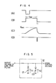
- Fig. 3 shows a circuit diagram showing a specific example of the monostable multivibrator 11 of voltage control type in Fig. 1, and Fig. 4 shows waveforms of various signals in Fig. 3.
- numerals 17 and 17' designate NAND gates, numerals 18 to 20 resistors, numeral 21 a capacitor, numeral 22 a comparator, and numeral 23 a transistor.
- Vc V (1 - )
- V B is the voltage at point B when it is “high”.
- the transistor 23 is cut off, and the charging operation of the capacitor 21 continues until Vc ecomes Vcont.
- Vc exceeds Vcont and the output D of the comparator 22 is reduced to "low”.
- the input terminal 17B of the NAND gate 17 shown by 17 is raised to "high”
- the output terminal 17C thereof is lowered to "low” state.
- the output terminal 17c of the NAND gate 17 is thus raised to "high”.
- the input terminal 17'A of the NAND gate 17' is raised to "high” (The second input terminal of NAND gate 17' namely, the terminal 32 is raised to "high” immediately after being reduced to “low” by the trigger. In other words, the second input terminal of the NAND gate 17' is raised to "high” at least before the output D is reduced to “low”.)
- the output B of the NAND gate 17 is reduced to "low”.
- T MW CR 1 In
- the circuit shown in Fig. 3 may be used as the monostable multivibrator 3 of voltage controlled type shown in Fig. 1.
- a control voltage limiter circuit 12 as shown in Fig. 5 is inserted between the low-pass filter 11 and the control terminal 31 for preventing the great variations of the duration of the output pulse under transient conditions. Also, the circuit 12 always maintain the control voltage between the voltage V 1 of the DC power supply 121 and the voltage V 2 of the DC power supply 12, and therefore by neglecting the asymmetric control range of the rise of the collector voltage ((F) in Fig. 2) (that is, by displacing the central vollage from ( ), the deflection frequency may be increased.
- the rise point of the drive transistor is controlled always most properly regardless of the storage time of the drive transistor or the variations thereof among transistor elements or the change thereof with temperature increase, and therefore the horizontal deflection frequency.is capable of being increased.
Landscapes
- Details Of Television Scanning (AREA)
Applications Claiming Priority (4)
| Application Number | Priority Date | Filing Date | Title |
|---|---|---|---|
| JP16584081A JPS5868370A (ja) | 1981-10-19 | 1981-10-19 | 水平偏向回路 |
| JP165840/81 | 1981-10-19 | ||
| JP178381/81 | 1981-11-09 | ||
| JP17838181A JPS5880971A (ja) | 1981-11-09 | 1981-11-09 | 水平偏向回路 |
Publications (3)
| Publication Number | Publication Date |
|---|---|
| EP0077565A2 true EP0077565A2 (fr) | 1983-04-27 |
| EP0077565A3 EP0077565A3 (en) | 1984-04-18 |
| EP0077565B1 EP0077565B1 (fr) | 1988-02-17 |
Family
ID=26490420
Family Applications (1)
| Application Number | Title | Priority Date | Filing Date |
|---|---|---|---|
| EP82109640A Expired EP0077565B1 (fr) | 1981-10-19 | 1982-10-19 | Circuit de déflexion horizontale |
Country Status (3)
| Country | Link |
|---|---|
| US (1) | US4442384A (fr) |
| EP (1) | EP0077565B1 (fr) |
| DE (1) | DE3278123D1 (fr) |
Cited By (1)
| Publication number | Priority date | Publication date | Assignee | Title |
|---|---|---|---|---|
| FR2570561A1 (fr) * | 1984-09-17 | 1986-03-21 | Tektronix Inc | Amplificateur de puissance fonctionnant a grande vitesse et utilisable pour la commande de charges inductives |
Families Citing this family (3)
| Publication number | Priority date | Publication date | Assignee | Title |
|---|---|---|---|---|
| DE3420312C2 (de) * | 1984-05-30 | 1986-10-09 | SGS Halbleiter-Bauelemente GmbH, 8018 Grafing | Ansteuerschaltung für einen Ablenk-Leistungstransistor |
| US4992708A (en) * | 1988-12-22 | 1991-02-12 | Victor Company Of Japan, Ltd. | Horizontal deflection and high voltage generating circuit |
| KR100203404B1 (ko) * | 1996-11-14 | 1999-06-15 | 윤종용 | 편향구동회로 |
Family Cites Families (4)
| Publication number | Priority date | Publication date | Assignee | Title |
|---|---|---|---|---|
| US3533009A (en) * | 1968-11-15 | 1970-10-06 | Ibm | Dual servo loop oscillator frequency synchronizing circuitry |
| FR2166753A5 (fr) * | 1972-01-07 | 1973-08-17 | Trt Telecom Radio Electr | |
| CA1013479A (en) * | 1973-09-03 | 1977-07-05 | Yoshinori Kitamura | Deflection system |
| NL7714033A (nl) * | 1977-12-19 | 1979-06-21 | Philips Nv | Televisie-ontvanger met een lijnsynchroniseer- schakeling. |
-
1982
- 1982-10-18 US US06/434,880 patent/US4442384A/en not_active Expired - Fee Related
- 1982-10-19 DE DE8282109640T patent/DE3278123D1/de not_active Expired
- 1982-10-19 EP EP82109640A patent/EP0077565B1/fr not_active Expired
Cited By (1)
| Publication number | Priority date | Publication date | Assignee | Title |
|---|---|---|---|---|
| FR2570561A1 (fr) * | 1984-09-17 | 1986-03-21 | Tektronix Inc | Amplificateur de puissance fonctionnant a grande vitesse et utilisable pour la commande de charges inductives |
Also Published As
| Publication number | Publication date |
|---|---|
| EP0077565B1 (fr) | 1988-02-17 |
| EP0077565A3 (en) | 1984-04-18 |
| US4442384A (en) | 1984-04-10 |
| DE3278123D1 (en) | 1988-03-24 |
Similar Documents
| Publication | Publication Date | Title |
|---|---|---|
| US5394020A (en) | Vertical ramp automatic amplitude control | |
| US3241023A (en) | Motor speed control | |
| US6369665B1 (en) | Maintaining constant amount of slope compensation regardless of switching frequency during synchronization | |
| US5013980A (en) | Voltage regulator in a television apparatus | |
| EP0077565A2 (fr) | Circuit de déflexion horizontale | |
| US4891608A (en) | #6 Control circuit for horizontal oscillator | |
| US4866525A (en) | Television apparatus power supply | |
| EP0030816B1 (fr) | Systèmes de signalisation pour alimentation électrique à courant alternatif | |
| US4803381A (en) | Bias current compensating circuit, particularly for saw-tooth wave generators | |
| KR940005259B1 (ko) | 수직 톱니파 발생회로 | |
| US3987371A (en) | Circuit arrangement including a synchronized oscillator that is stable with respect to temperature and voltage variations | |
| US5877640A (en) | Device for deriving a clock signal from a synchronizing signal and a videorecorder provided with the device | |
| US4617509A (en) | Voltage regulator for a microcomputer system | |
| US4789896A (en) | Vertical synchronizing pulse generating circuit | |
| US4385320A (en) | Automatic frequency control circuit | |
| JPS6322591B2 (fr) | ||
| US4742313A (en) | Phase-locked loop circuit having a mechanism for preventing erroneous operation | |
| US3947724A (en) | Variable-frequency sweep generator circuit | |
| US4334174A (en) | Sawtooth waveform generation for a television receiver | |
| KR950003343B1 (ko) | 시간기록유지장치 및 그 기록유지방법 | |
| JP2535851B2 (ja) | 鋸歯状波信号発生回路 | |
| US4126815A (en) | Delayed kinescope blanking pulse generator | |
| JP2521055B2 (ja) | 水平偏向回路 | |
| US6226344B1 (en) | Generation of a time period | |
| JPS6236382Y2 (fr) |
Legal Events
| Date | Code | Title | Description |
|---|---|---|---|
| PUAI | Public reference made under article 153(3) epc to a published international application that has entered the european phase |
Free format text: ORIGINAL CODE: 0009012 |
|
| AK | Designated contracting states |
Designated state(s): DE FR GB |
|
| PUAL | Search report despatched |
Free format text: ORIGINAL CODE: 0009013 |
|
| AK | Designated contracting states |
Designated state(s): DE FR GB |
|
| 17P | Request for examination filed |
Effective date: 19840831 |
|
| GRAA | (expected) grant |
Free format text: ORIGINAL CODE: 0009210 |
|
| AK | Designated contracting states |
Kind code of ref document: B1 Designated state(s): DE FR GB |
|
| REF | Corresponds to: |
Ref document number: 3278123 Country of ref document: DE Date of ref document: 19880324 |
|
| ET | Fr: translation filed | ||
| PLBE | No opposition filed within time limit |
Free format text: ORIGINAL CODE: 0009261 |
|
| STAA | Information on the status of an ep patent application or granted ep patent |
Free format text: STATUS: NO OPPOSITION FILED WITHIN TIME LIMIT |
|
| 26N | No opposition filed | ||
| PGFP | Annual fee paid to national office [announced via postgrant information from national office to epo] |
Ref country code: FR Payment date: 19900831 Year of fee payment: 9 |
|
| PGFP | Annual fee paid to national office [announced via postgrant information from national office to epo] |
Ref country code: GB Payment date: 19900907 Year of fee payment: 9 |
|
| PGFP | Annual fee paid to national office [announced via postgrant information from national office to epo] |
Ref country code: DE Payment date: 19901128 Year of fee payment: 9 |
|
| PG25 | Lapsed in a contracting state [announced via postgrant information from national office to epo] |
Ref country code: GB Effective date: 19911019 |
|
| GBPC | Gb: european patent ceased through non-payment of renewal fee | ||
| PG25 | Lapsed in a contracting state [announced via postgrant information from national office to epo] |
Ref country code: FR Effective date: 19920630 |
|
| PG25 | Lapsed in a contracting state [announced via postgrant information from national office to epo] |
Ref country code: DE Effective date: 19920701 |
|
| REG | Reference to a national code |
Ref country code: FR Ref legal event code: ST |