EP0077601A2 - Photovoltaische Halbleitereinrichtung - Google Patents
Photovoltaische Halbleitereinrichtung Download PDFInfo
- Publication number
- EP0077601A2 EP0077601A2 EP82303096A EP82303096A EP0077601A2 EP 0077601 A2 EP0077601 A2 EP 0077601A2 EP 82303096 A EP82303096 A EP 82303096A EP 82303096 A EP82303096 A EP 82303096A EP 0077601 A2 EP0077601 A2 EP 0077601A2
- Authority
- EP
- European Patent Office
- Prior art keywords
- layer
- amorphous silicon
- doped
- intrinsic
- onto
- Prior art date
- Legal status (The legal status is an assumption and is not a legal conclusion. Google has not performed a legal analysis and makes no representation as to the accuracy of the status listed.)
- Withdrawn
Links
Images
Classifications
-
- H—ELECTRICITY
- H10—SEMICONDUCTOR DEVICES; ELECTRIC SOLID-STATE DEVICES NOT OTHERWISE PROVIDED FOR
- H10F—INORGANIC SEMICONDUCTOR DEVICES SENSITIVE TO INFRARED RADIATION, LIGHT, ELECTROMAGNETIC RADIATION OF SHORTER WAVELENGTH OR CORPUSCULAR RADIATION
- H10F71/00—Manufacture or treatment of devices covered by this subclass
- H10F71/10—Manufacture or treatment of devices covered by this subclass the devices comprising amorphous semiconductor material
- H10F71/103—Manufacture or treatment of devices covered by this subclass the devices comprising amorphous semiconductor material including only Group IV materials
-
- H—ELECTRICITY
- H10—SEMICONDUCTOR DEVICES; ELECTRIC SOLID-STATE DEVICES NOT OTHERWISE PROVIDED FOR
- H10F—INORGANIC SEMICONDUCTOR DEVICES SENSITIVE TO INFRARED RADIATION, LIGHT, ELECTROMAGNETIC RADIATION OF SHORTER WAVELENGTH OR CORPUSCULAR RADIATION
- H10F10/00—Individual photovoltaic cells, e.g. solar cells
- H10F10/10—Individual photovoltaic cells, e.g. solar cells having potential barriers
- H10F10/17—Photovoltaic cells having only PIN junction potential barriers
-
- Y—GENERAL TAGGING OF NEW TECHNOLOGICAL DEVELOPMENTS; GENERAL TAGGING OF CROSS-SECTIONAL TECHNOLOGIES SPANNING OVER SEVERAL SECTIONS OF THE IPC; TECHNICAL SUBJECTS COVERED BY FORMER USPC CROSS-REFERENCE ART COLLECTIONS [XRACs] AND DIGESTS
- Y02—TECHNOLOGIES OR APPLICATIONS FOR MITIGATION OR ADAPTATION AGAINST CLIMATE CHANGE
- Y02E—REDUCTION OF GREENHOUSE GAS [GHG] EMISSIONS, RELATED TO ENERGY GENERATION, TRANSMISSION OR DISTRIBUTION
- Y02E10/00—Energy generation through renewable energy sources
- Y02E10/50—Photovoltaic [PV] energy
- Y02E10/548—Amorphous silicon PV cells
-
- Y—GENERAL TAGGING OF NEW TECHNOLOGICAL DEVELOPMENTS; GENERAL TAGGING OF CROSS-SECTIONAL TECHNOLOGIES SPANNING OVER SEVERAL SECTIONS OF THE IPC; TECHNICAL SUBJECTS COVERED BY FORMER USPC CROSS-REFERENCE ART COLLECTIONS [XRACs] AND DIGESTS
- Y02—TECHNOLOGIES OR APPLICATIONS FOR MITIGATION OR ADAPTATION AGAINST CLIMATE CHANGE
- Y02P—CLIMATE CHANGE MITIGATION TECHNOLOGIES IN THE PRODUCTION OR PROCESSING OF GOODS
- Y02P70/00—Climate change mitigation technologies in the production process for final industrial or consumer products
- Y02P70/50—Manufacturing or production processes characterised by the final manufactured product
Definitions
- the present invention relates to a photovoltaic semiconductor device, and in one embodiment to a PIN amorphous silicon semiconductor device having particularly constructed p and n regions to improve the photovoltaic output of the device.
- Hydrogenated amorphous silicon is a promising candidate for thin film semiconductor applications, and in particular thin film photovoltaic applications.
- the discovery that an amount of hydrogen incorporated into the bonding structure of the amorphous silicon thin film results in a substantial increase in the photoconductivity of the semiconductor brought numerous applications of this material to the art.
- One of the more successful photovoltaic applications of amorphous silicon is the configuration generally referred to as a PIN structure.
- PIN structure refers to the semiconductor structure having an intrinsic (updoped) region of semiconductor material disposed between an n-doped region and a p-doped region of the semiconductor material.
- the structure is recognized as resulting in higher Voc and I sc as compared to p-n junctions or the like.
- the present invention is directed to a PIN homojunction whose particular construction of the P & N regions results in a substantial enhancement in the photogeneration of charge carriers, and device output.
- the glow discharge deposition produces a p-layer which is both poorly conductive and absorbs the incident light energy without significantly contributing to the photogeneration of the charge carriers in the device.
- the poorer electronic properties of the p-layer originate from Boron incorporation into the network that introduces defect states in the gap of the semiconductor, which act as recombination centres. In addition, these defect states induce optical absorption which make the effective optical gap of the p-layer to be smaller than that of the I-layer.
- a photovoltaic semiconductor device comprising a multi-layer structure consisting at least of a layer of intrinsic amorphous silicon between a layer of n-doped amorphous silicon and a layer of p-doped amorphous silicon, characterised in that the p-doped layer is reactively sputtered onto an adjacent layer.
- embodiments of the present invention teach an amorphous silicon PIN device having a p-region which is particularly constructed to have a wide band gap resulting in a substantial transmission of light energy to the intrinsic layer. Furthermore, the construction techniques as taught herein, result in a p-region. Embodiments of the invention further include a particularly adapted construction of both the p- and n-layer to control -the band gap of same, -which should result in an increase in the open circuit voltage produced by the photovoltaic device.
- a hybrid construction amorphous silicon PIN device may have an intrinsic (undoped) layer produced by glow discharged decomposition of silane while having at least the p-doped region constructed by reactive sputtering from a Si target in a plasma of Argon and hydrogen.
- the hybrid construction results in the ability to control the optical band gap of the p and n layers resulting in both an increased open circuit voltage, and in the case of the controlled optical band gap for the p-layer overcoming the long standing deficiency of absorption without substantial carrier generation by the p-layer.
- An attendant advantage in the construction of the p-layer is enhanced photogeneration of charge carriers within the p-layer itself.
- the p-layer has a band gap larger than about 1.8 ev, for example about 1.8 ev to about 2.0 ep.
- the p-layer may be reactively sputtered onto the intrinsic layer to form a semiconductor junction therewith.
- the p-layer may be reactively sputtered onto a conductive layer of said multi-layer structure to provide ohmic contact therewith.
- One embodiment of the invention provides a PIN photovoltaic device having a body of hydrogenated amorphous silicon, said device comprising: a substrate;
- a method of producing a photovoltaic semiconductor device comprising a multi-layer structure consisting at least of a layer of intrinsic amorphous silicon between a layer of n-doped amorphous silicon and a layer of p-doped amorphous silicon, said method being characterised by reactively sputtering said p-layer onto an adjacent layer as one step in building-up said multi-layer structure by successive layer deposition.
- the p-layer may be reactively sputtered in partial pressures of hydrogen and argon ranging from about 0.5 mTorr to about 2.0 mTorr and for about 3.0 mTorr to -about 15.0 mTorr, respectively.
- the p-layer is sputtered while applying a DC bias, ranging from about 0 volts to about +100 volts, to a substrate provided with a conductive layer which is said adjacent layer, or to the said substrate, as the case may be.
- a DC bias ranging from about 0 volts to about +100 volts
- the n-doped layer of amorphous silicon may be deposited by low discharge decomposition of phosphine doped silane or sputtering in a plasma containing Ar + H 2 + PH 3 .
- the photovoltaic device may be such that light incident on the p-layer of wavelength in the region of 6000 to 4000 A passes substantially unabsorbed through the p-layer to be absorbed by the intrinsic layer.
- the intrinsic layer of amorphous silicon can suitably be deposited by glow discharge decomposition of silane.
- the p-doped layer may range in thickness from about 80 ⁇ . to about 200 A.
- a further aspect of the invention contemplates a photovoltaic semiconductor PIN or NIP device whose layers are built up sequentially by sputtering and glow discharge alternately. This construction enables the electrons activated by the impinging photons to pass through unimpeded rather than becoming trapped and thereby being unable to produce inadequate electrical output.
- a first embodiment of the present invention is directed to an improved amorphous silicon PIN device having increased photovoltaic response as evidenced by enhanced photo output in the blue spectral region.
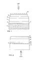
- FIG 1 there is shown a greatly enlarged side view of a PIN device.
- a substrate 10 generally comprises a physically supportive substrate for overlying layers of thin films.
- the substrate 10 includes a major area coating surface which is substantially free from voids or protrusions of the order (in size) of the thickness of the overlying layers, discussed hereinafter, to avoid pinholes therethrough.
- substrate 10 is illustrated as comprising a generally nontransparent material.
- substrate 10 may comprise a non-electroconductive material such as a ceramic, for example, for which an overlying layer of electroconductive material 11 is required.
- substrate 10 may comprise a metal serving both as a supportive substrate and as a current carrying electrode in the operation of the photovoltaic device. In either instance, the coating surface of the substrate is thoroughly cleaned to remove unwanted contamination and particulate from the coating surface.
- electrode 10 comprises a metal known to form an ohmic contact to n-doped silicon such as molybdenum or stainless steel for example.
- layer 11 comprise a layer of metal known to form an ohmic contact to n-doped amorphous silicon such as the aforementioned molybdenum or chromium which may be deposited onto the substrate to a thickness of approximately 1,000 to 2,000 R.
- Layer 12 comprises N-doped hydrogenated amorphous silicon, ranging in thickness from about 100 A to about 1000 ⁇ , deposited onto the coating surface of the substrate.
- the term N-doped as described in relation to the art of hydrogenated amorphous silicon may be defined as a film of amorphous silicon which includes electronically acting dopants such as phosphorous, arsenic, and antimony which serve to move the Fermi level closer to the conduction band, thus enhancing the conductivity of the film.
- N-doped layer 12 may be fabricated by the alternate techniques of reactive sputtering or glow discharge.
- An n-doped layer of hydrogenated amorphous silicon can be constructed by the glow discharge decomposition of silane containing an amount of phosphine doping gas.
- the deposition process includes the steps of first heating the substrate to a temperature of 200-400°C.
- the substrate can be sputter-etched in an Ar discharge to effect further cleaning.
- the feed gas consisting of .1 to 1% PH 3 in Si H 4 is then fed into the reactor and the pressure raised to the desired level, usually 10 to 1000 mTorr. Either DC or RF power is then applied to effect ionization of the gases.
- the film is allowed to grow to the desired thickness, usually 100-1000 ⁇ , after which the power is removed.
- the conductivity of these films are generally 10 -2 ⁇ -1 cm -1 and their optical gap is smaller than the corresponding intrinsic film. [Eg (intrinsic) 1.7 ev, Eg (n-layer) ⁇ 1.7 ev.]
- the n-layer of hydrogenated amorphous silicon may be constructed by reactive sputtering in partial pressures of hydrogen, argon and phosphine.
- the process of sputtering the n-layer includes: First heating the substrate to a temperature of 200 to 400°C. Both the target and the substrate are sputter-etched in an argon plasma. A gas mixture of phosphine, hydrogen and argon is established in the sputtering chamber.
- the phosphine partial pressure ranges from 5 x 10- 6 to 5 x 10- 5 Torr
- the hydrogen partial pressure ranges from 5 x 10- 4 to 2.0 x 10- 3 Torr
- the argon partial pressure ranges from 3 x 10- 3 to 15 x 10- 3 Torr.
- the silicon target 5 inches in diameter, is supplied with an RF power of between 100 to 300 watts.
- the film is allowed to grow to the desired thickness, usually between 100 to 1000 R.
- the conductivity of these films is about 10- 2 ⁇ -1 cm-l and their optical gap varies between 1.6 to 1.90 eV depending on the amount of incorporated hydrogen.
- An intrinsic layer of hydrogenated amorphous silicon 14 comprises undoped amorphous silicon, ranging in thickness from about .2 microns to about 10 microns, deposited by the glow discharge decomposition of substantially undoped silane.
- the term intrinsic defines a region of amorphous silicon which is characterized as one containing a minimum of impurities such that the electronic properties are determined by the structure and Si and H content of the film. Good intrinsic films may also be defined as having a low density of states in the gap which indicates good structural properties.
- the construction of the intrinsic layer 14 by glow discharge decomposition of silane may be generally described as including the steps of first elevating the substrate temperature to between desired level, usually 200-400°C.
- the SiH 4 fuel is then fed into the reactor and the pressure brought to the desired level, usually 10-1000 mT. Either DC or RF power is then applied to start a glow discharge. The film is then allowed to grow to the desired thickness, usually .2-10 ⁇ m, after which the power is removed.
- a layer of p-doped hydrogenated amorphous silicon 16 having a particularly adapted construction process as to provide control of the optical band gap of the material is disposed onto intrinsic layer 14.
- the term p-doped as defined in relation to the art of hydrogenated amorphous silicon is characterized as a film of a-Si which contains electronically active dopants such as boron which serve to move the fermi level closer to the valance band thus enhancing the conductivity of the film.
- the p-layer ranging in thickness from about 80 R to about 300 R, is reactively sputtered from a polycrystalline silicon target in partial pressures of hydrogen, argon and diborane. The process of sputtering the p-layer includes the following steps.
- the three gases are premixed at certain partial pressures.
- the partial pressure of diborane ranges between 5 x 10⁻⁶ to 5 x 10⁻⁵ Torr; the partial pressure of hydrogen ranges between 0.5 to 2.0 mTorr and the partial pressure of argon ranges between 3 to 15 mTorr.
- the sputtering power conditions are identical to those described for the deposition of the n-layer.
- the conductivity of these film are between 10-3 to 10- 2 ⁇ -1 cm- 1 and their optical gap is larger than 1.8 ev.
- the particularly adapted construction of the p-layer of hydrogenated amorphous silicon results in a p-layer which not only enhances the open circuit voltage of the device as recognized by others in the art, but further provides a semiconductor "window layer", passing a substantial amount of incident light therethrough, to be absorbed in the highly photogenerative region of the underlying I-layer.
- the construction of the wide band gap p-layer as taught herein is accomplished without substantial addition of defect states to the amorphous silicon hydride preserving a high carrier lifetime of the layer and providing for a relatively bigh efficiency of boron doping of the region.
- An ohmic electrode 18 may include a transparent conductive oxide such as indium tin oxide, cadmium stanate, or tin oxide. These n-type semiconductor oxides are recognized by those in the art as forming an ohmic contact to, relatively heavily doped p-type amorphous silicon. Additionally, it is recognized that the refractive indices of these oxides provide a relatively good index of refraction matching to the surface of the p-type amorphous silicon resulting in an anti-reflection coating.
- electrode 18 comprises a layer of indium tin oxide reactively sputtered from a sputtering target 5 inches in diameter and having a composition of In 2 0 3/ 9M% Sn0 2 .
- the target is supplied with a power of 50 watts.
- the substrate is heated to about 250 o C.
- the thickness of the ITO layer is chosen to be between 500 to 700 R.
- the electroconductivity of layer 18 may be supplemented by a grid 20 comprising a highly electroconductive material, such as a noble metal for instance.
- Means for optimizing the grid pattern, grid thickness, and the means for constructing the grid itself, are well-known in the art of photovoltaic devices.
- Layers 12 and 16 in Figure 1 may be inverted. In this case, the p-Layer is sputtered first, followed by the glow discharge I-layer and the sputtered (or glow discharge) n-layer. The layer 18 and 20 remain the same.
- a substantially transparent substrate 30 permits illumination of the device through the substrate.
- substrate 30 is selected from materials exhibiting substantial transparency to light energy of wavelengths ranging from about .3 microns to about 2.0 microns. Suitable materials for use in substrate 30 include glass, quartz and saphire, for example.
- the coating surface of substrate 30 is scrupulously cleaned to remove particulate etc which may result in pinholes through the overlying thin film layers.
- a semitransparent conductive oxide layer 32 is deposited on the substrate 30. The conductive oxide is chosen to provide an ohmic contact to a layer p-doped amorphous silicon deposited thereon.
- the'conductivity of layer 32 may be supplemented by grid layer 31, comprising a highly electroconductive metal, for example, nichrome, silver, etc.
- a layer of p-doped hydrogenated amorphous silicon 34 is reactively sputtered onto the surface of layer 32.
- the thickness of this layer is generally 100 ⁇ .
- the deposition parameters for layer 34 are substantially identical to those described for the p-layer of the previous embodiment illustrated as layer 16 of Figure 1.
- n-doped layer of hydrogenated amorphous silicon 38 is deposited onto intrinsic layer 36 to a thickness ranging from about 200 A to about 500 ⁇ , the intrinsic layer 36 itself having been deposited on the p-layer 34.
- the constructions of the intrinsic layer 36 and the n-doped layer 33 are substantially identical to the intrinsic and n-doped layers, respectively described in the previous embodiment.
- An ohmic contact 40 is selected from materials known to form an ohmic contact with n-doped amorphous silicon, including chromium, molybdenum, etc. These layers are deposited either by evaporation or sputtering.
- the particularly adapted construction of the p-doped layer 34 results in a wide band gap semiconductor having improved photogeneration and doping efficiency characteristics resulting in an amorphous silicon PIN device, having both increased open circuit voltage and enhanced blue response.
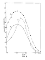
- traces B and C a collection efficiency spectra generally characterising the spectral photo-response of prior art PIN devices illuminated from the P-side. Shown in contrast thereto is spectrum A of an improved PIN device constructed in accordance with the present invention, exhibiting substantially increased photo-response in the whole wavelength region.
Landscapes
- Photovoltaic Devices (AREA)
Applications Claiming Priority (2)
| Application Number | Priority Date | Filing Date | Title |
|---|---|---|---|
| US06/311,546 US4407710A (en) | 1981-10-15 | 1981-10-15 | Hybrid method of making an amorphous silicon P-I-N semiconductor device |
| US311546 | 1981-10-15 |
Publications (2)
| Publication Number | Publication Date |
|---|---|
| EP0077601A2 true EP0077601A2 (de) | 1983-04-27 |
| EP0077601A3 EP0077601A3 (de) | 1984-10-03 |
Family
ID=23207390
Family Applications (1)
| Application Number | Title | Priority Date | Filing Date |
|---|---|---|---|
| EP82303096A Withdrawn EP0077601A3 (de) | 1981-10-15 | 1982-06-15 | Photovoltaische Halbleitereinrichtung |
Country Status (5)
| Country | Link |
|---|---|
| US (1) | US4407710A (de) |
| EP (1) | EP0077601A3 (de) |
| JP (1) | JPS5873169A (de) |
| AU (1) | AU548005B2 (de) |
| CA (1) | CA1187588A (de) |
Families Citing this family (9)
| Publication number | Priority date | Publication date | Assignee | Title |
|---|---|---|---|---|
| US4527179A (en) * | 1981-02-09 | 1985-07-02 | Semiconductor Energy Laboratory Co., Ltd. | Non-single-crystal light emitting semiconductor device |
| JPS59108370A (ja) * | 1982-12-14 | 1984-06-22 | Kanegafuchi Chem Ind Co Ltd | 光起電力装置 |
| GB2137810B (en) * | 1983-03-08 | 1986-10-22 | Agency Ind Science Techn | A solar cell of amorphous silicon |
| US4529619A (en) * | 1984-07-16 | 1985-07-16 | Xerox Corporation | Ohmic contacts for hydrogenated amorphous silicon |
| US5273919A (en) * | 1985-06-20 | 1993-12-28 | Canon Kabushiki Kaisha | Method of producing a thin film field effect transistor |
| EP0275446A1 (de) * | 1986-12-19 | 1988-07-27 | Heimann GmbH | Röntgenstrahlendetektor |
| JP2907128B2 (ja) * | 1996-07-01 | 1999-06-21 | 日本電気株式会社 | 電界効果型トランジスタ及びその製造方法 |
| JP5857237B2 (ja) * | 2010-11-29 | 2016-02-10 | パナソニックIpマネジメント株式会社 | 太陽電池セル及び太陽電池モジュール |
| US9112103B1 (en) | 2013-03-11 | 2015-08-18 | Rayvio Corporation | Backside transparent substrate roughening for UV light emitting diode |
Family Cites Families (5)
| Publication number | Priority date | Publication date | Assignee | Title |
|---|---|---|---|---|
| US4064521A (en) * | 1975-07-28 | 1977-12-20 | Rca Corporation | Semiconductor device having a body of amorphous silicon |
| US4342044A (en) * | 1978-03-08 | 1982-07-27 | Energy Conversion Devices, Inc. | Method for optimizing photoresponsive amorphous alloys and devices |
| FR2461763A1 (fr) * | 1979-07-20 | 1981-02-06 | Commissariat Energie Atomique | Procede d'elaboration de couches de silicium amorphe fluore par la methode de pulverisation cathodique |
| US4339470A (en) * | 1981-02-13 | 1982-07-13 | Rca Corporation | Fabricating amorphous silicon solar cells by varying the temperature _of the substrate during deposition of the amorphous silicon layer |
| US4417092A (en) * | 1981-03-16 | 1983-11-22 | Exxon Research And Engineering Co. | Sputtered pin amorphous silicon semi-conductor device and method therefor |
-
1981
- 1981-10-15 US US06/311,546 patent/US4407710A/en not_active Expired - Fee Related
-
1982
- 1982-06-08 AU AU84667/82A patent/AU548005B2/en not_active Ceased
- 1982-06-15 EP EP82303096A patent/EP0077601A3/de not_active Withdrawn
- 1982-06-15 JP JP57101530A patent/JPS5873169A/ja active Pending
- 1982-06-17 CA CA000405405A patent/CA1187588A/en not_active Expired
Also Published As
| Publication number | Publication date |
|---|---|
| AU548005B2 (en) | 1985-11-14 |
| CA1187588A (en) | 1985-05-21 |
| AU8466782A (en) | 1983-04-21 |
| US4407710A (en) | 1983-10-04 |
| JPS5873169A (ja) | 1983-05-02 |
| EP0077601A3 (de) | 1984-10-03 |
Similar Documents
| Publication | Publication Date | Title |
|---|---|---|
| EP0523919B1 (de) | Photovoltische Vorrichtung mit mehreren Übergängen und Herstellungsverfahren | |
| JP2695585B2 (ja) | 光起電力素子及びその製造方法、並びにそれを用いた発電装置 | |
| EP1271661B1 (de) | Photovoltaische Vorrichtung | |
| US7879644B2 (en) | Hybrid window layer for photovoltaic cells | |
| US5032884A (en) | Semiconductor pin device with interlayer or dopant gradient | |
| EP0111247B1 (de) | Fotovoltaische Anordnung | |
| AU734676B2 (en) | Photovoltaic element and method of producing same | |
| US4528082A (en) | Method for sputtering a PIN amorphous silicon semi-conductor device having partially crystallized P and N-layers | |
| EP0831538A2 (de) | Photovoltaisches Bauelement mit einer spezifisch dotierten Schicht | |
| US4398054A (en) | Compensated amorphous silicon solar cell incorporating an insulating layer | |
| JP2006080557A (ja) | 高水素希釈低温プラズマ蒸着によって製造されるアモルファスシリコン系素子の向上せしめられた安定化特性 | |
| GB2124826A (en) | Amorphous semiconductor materials | |
| EP1372198A2 (de) | Photovoltaische Vorrichtung | |
| US4528418A (en) | Photoresponsive semiconductor device having a double layer anti-reflective coating | |
| US5769963A (en) | Photovoltaic device | |
| US4396793A (en) | Compensated amorphous silicon solar cell | |
| EP0500067B1 (de) | Photovoltaische Vorrichtung mit einer Germanium enthaltenden Schichtzone | |
| EP0077601A2 (de) | Photovoltaische Halbleitereinrichtung | |
| US5104455A (en) | Amorphous semiconductor solar cell | |
| EP0437767A1 (de) | Erhöhung des Kurzschlussstroms durch Benutzung einer n-Schicht mit grosser Bandlücke in p-i-n photovoltaischen Zellen aus amorphem Silizium | |
| CN118476039A (zh) | 太阳能电池及其形成方法 | |
| KR810001314B1 (ko) | 비결정 실리콘 활성영역을 갖는 반도체 장치 | |
| JP2545066B2 (ja) | 半導体装置 | |
| TWI453929B (zh) | 太陽能模組及製造具有並聯半導體層堆疊之太陽能模組之方法 | |
| JPH0799777B2 (ja) | 非晶質半導体素子 |
Legal Events
| Date | Code | Title | Description |
|---|---|---|---|
| PUAI | Public reference made under article 153(3) epc to a published international application that has entered the european phase |
Free format text: ORIGINAL CODE: 0009012 |
|
| AK | Designated contracting states |
Designated state(s): DE FR GB IT |
|
| PUAL | Search report despatched |
Free format text: ORIGINAL CODE: 0009013 |
|
| AK | Designated contracting states |
Designated state(s): DE FR GB IT |
|
| 17P | Request for examination filed |
Effective date: 19850306 |
|
| 17Q | First examination report despatched |
Effective date: 19860610 |
|
| STAA | Information on the status of an ep patent application or granted ep patent |
Free format text: STATUS: THE APPLICATION IS DEEMED TO BE WITHDRAWN |
|
| 18D | Application deemed to be withdrawn |
Effective date: 19861223 |
|
| RIN1 | Information on inventor provided before grant (corrected) |
Inventor name: ABELES, BENJAMIN Inventor name: MOREL, DON LOUIS Inventor name: MOUSTAKAS, THEODORE DEMETRI |