EP0077900B1 - Dispositif enregistreur de données sur un support - Google Patents
Dispositif enregistreur de données sur un support Download PDFInfo
- Publication number
- EP0077900B1 EP0077900B1 EP82107876A EP82107876A EP0077900B1 EP 0077900 B1 EP0077900 B1 EP 0077900B1 EP 82107876 A EP82107876 A EP 82107876A EP 82107876 A EP82107876 A EP 82107876A EP 0077900 B1 EP0077900 B1 EP 0077900B1
- Authority
- EP
- European Patent Office
- Prior art keywords
- electrodes
- writing
- contact
- comb
- current supply
- Prior art date
- Legal status (The legal status is an assumption and is not a legal conclusion. Google has not performed a legal analysis and makes no representation as to the accuracy of the status listed.)
- Expired
Links
- 239000000853 adhesive Substances 0.000 claims description 8
- 238000000034 method Methods 0.000 claims description 7
- 230000001070 adhesive effect Effects 0.000 claims description 6
- 239000004020 conductor Substances 0.000 claims description 5
- 238000004519 manufacturing process Methods 0.000 claims description 5
- 230000005855 radiation Effects 0.000 claims description 4
- 238000005299 abrasion Methods 0.000 claims description 2
- 239000011248 coating agent Substances 0.000 claims description 2
- 238000000576 coating method Methods 0.000 claims description 2
- 239000011888 foil Substances 0.000 claims description 2
- 239000011159 matrix material Substances 0.000 claims description 2
- 239000011241 protective layer Substances 0.000 claims description 2
- 238000007650 screen-printing Methods 0.000 claims description 2
- 239000002184 metal Substances 0.000 claims 1
- 238000001465 metallisation Methods 0.000 claims 1
- 238000001771 vacuum deposition Methods 0.000 claims 1
- 238000004804 winding Methods 0.000 description 6
- 238000009413 insulation Methods 0.000 description 5
- 238000003466 welding Methods 0.000 description 4
- 239000011810 insulating material Substances 0.000 description 3
- 230000006978 adaptation Effects 0.000 description 2
- 230000001427 coherent effect Effects 0.000 description 2
- 238000005516 engineering process Methods 0.000 description 2
- 239000010410 layer Substances 0.000 description 2
- 238000005452 bending Methods 0.000 description 1
- 238000005266 casting Methods 0.000 description 1
- 230000001419 dependent effect Effects 0.000 description 1
- 238000011161 development Methods 0.000 description 1
- 230000018109 developmental process Effects 0.000 description 1
- 238000000454 electroless metal deposition Methods 0.000 description 1
- 238000010894 electron beam technology Methods 0.000 description 1
- 230000003628 erosive effect Effects 0.000 description 1
- 239000011347 resin Substances 0.000 description 1
- 229920005989 resin Polymers 0.000 description 1
- 229910052709 silver Inorganic materials 0.000 description 1
- 239000004332 silver Substances 0.000 description 1
- 229920001169 thermoplastic Polymers 0.000 description 1
- 239000004416 thermosoftening plastic Substances 0.000 description 1
- 238000007738 vacuum evaporation Methods 0.000 description 1
Images

Classifications
-
- B—PERFORMING OPERATIONS; TRANSPORTING
- B41—PRINTING; LINING MACHINES; TYPEWRITERS; STAMPS
- B41J—TYPEWRITERS; SELECTIVE PRINTING MECHANISMS, i.e. MECHANISMS PRINTING OTHERWISE THAN FROM A FORME; CORRECTION OF TYPOGRAPHICAL ERRORS
- B41J2/00—Typewriters or selective printing mechanisms characterised by the printing or marking process for which they are designed
- B41J2/385—Typewriters or selective printing mechanisms characterised by the printing or marking process for which they are designed characterised by selective supply of electric current or selective application of magnetism to a printing or impression-transfer material
- B41J2/39—Typewriters or selective printing mechanisms characterised by the printing or marking process for which they are designed characterised by selective supply of electric current or selective application of magnetism to a printing or impression-transfer material using multi-stylus heads
- B41J2/395—Structure of multi-stylus heads
Definitions
- the invention relates to a device for recording information on a record carrier according to the preamble of claim 1.
- One end of the adjacent wire electrodes are pressed between two opposite plates and thus form the write head.
- the other ends of the write electrodes of the film are divided into several groups for connection to a drive circuit.
- the electrodes of each group are connected to a circuit card.
- the circuit cards with the respective wire sections are rotated and bent so that they can be plugged into a control circuit. With this type of contact, the electrodes themselves can be damaged by twisting and bending the groups of electrodes. In addition, a larger space is required to accommodate the circuit cards.
- a method for manufacturing a write head in which the electrode wire is placed at a defined distance on an insulating plate.
- the insulating material plate has staggered outward connecting wires which are contacted by spot welding, resistance welding, laser beam welding or electron beam welding with the electrode wire at mutually offset locations.
- the arrangement is cast in casting resin, the ends of the electrode wire protruding from the encapsulated insulating material body and the connecting wires protruding from the encapsulated insulating material body approximately as perpendicular to the axis of the writing electrodes as plug pins.
- a write head produced according to this method has the disadvantage that a defined distance between the electrodes is necessary so that contact of only one electrode wire with the respective connecting wire is ensured.
- the distance between the electrodes depends on the width of the connector pins. In this known arrangement, it is therefore not possible to make the distance between the writing electrodes as narrow as possible.
- the object of the invention is therefore to provide a device for recording information on a record carrier in a compact design, in which to increase the resolution, the distance between the electrodes of the writing comb can be reduced to the thickness of their insulation, regardless of the contacting, and in which any number of electrodes can be arranged side by side without the space requirement is increased significantly due to the contact.
- any narrowly arranged writing electrodes and any number of writing electrodes arranged side by side can be contacted.
- the dimensions of the contact areas forming a grid-shaped contact field are not dependent on the thickness of an electrode or the distance between the electrodes, since they can extend over several electrodes.
- the manufacturing process for the contact surfaces is therefore based on wide tolerances.
- control circuit in a plane above the write comb achieves a compact design, the contact surfaces of the write comb being connected to the control circuit via releasable contacts, for example contact springs.
- This compact structure can be further reduced if the drive circuit, which is preferably built in integrated or hybrid technology, is connected to the write comb via fixed contacts, so that a very small, coherent unit of write comb drive circuit results.
- the resilient arrangement of the electrodes in the direction of the recording medium enables adaptation to unevenness in the recording medium and adaptation to the erosion of the electrodes.
- a constant accuracy of the recording is achieved by fixing the electrodes across the recording medium with the help of the highly flexible tape.
- the current By supplying current via electrodes which are located on the actual write head and are mechanically identical to the write electrodes, the current can be applied to the recording medium over a large area, so that the current supply electrodes do not mark on the recording medium.
- the power supply electrodes are subject to wear similar to that of the writing electrodes and can be replaced at the same time.
- the design of the electrodes as a coaxial conductor, in which the inner conductor forms the writing electrode and the current is supplied via the outer conductor, ensures an exact limitation of the writing point and the interference radiation generated by the writing spark is fully shielded.
- the control of the electrodes by Kon Constant current which limits the electrode current to a fixed value, increases the life of the electrodes. In addition, the entire control circuit is protected against incorrect operation.
- the writing comb can also be used for a thermal writing head. It is advantageous that all writing points are movable and can compensate for unevenness.
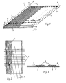
- FIG. 1 shows a writing comb 1 as used for a device for recording information.
- a large number of insulated wires 3 lying next to one another are fastened on a film 2, which can be designed, for example, as a Pertinax film, with the aid of an adhesive.
- the manufacture of such a wire-foil arrangement can be pushed using a winding device.
- a winding drum is used, which carries the film 2 provided with the adhesive.
- the insulated wire is continuously wound onto the film 2 by a rotating roller via a wire guide device which moves parallel to the axis of the winding drum during the winding process, a wire cylinder being formed.
- This wire cylinder is then cut open and processed into a writing comb 1 corresponding to FIG. 1.
- the adjacent wires 3 form the electrodes 4.
- a grid-shaped contact field is provided on the electrodes 4, which is formed by a multiplicity of contact surfaces 5.
- Fig. 2 shows the arrangement of the grid-shaped contact field.
- rows 6 parallel to the electrodes 4 and columns 7 parallel to the elongated electrodes 4 are provided somewhat obliquely.
- the contact areas 5 are formed at the crossing points of the row and column lines.
- the contact field thus has a multiplicity of parallel contact surface lines arranged transversely to the writing electrodes 4, the contact surfaces 5 of one contact surface line being somewhat offset from the contact surfaces of the previous line.
- contact surfaces 5 and electrodes 4 The contacting between contact surfaces 5 and electrodes 4 is shown with reference to FIG. 3. Each contact area 5 extends over several electrodes 4, of which only one electrode 8 is stripped. When stripping, the insulation of the very close-lying cable must not be damaged. Therefore, the wire 3 for the electrodes 4 is stripped in the winding process described above at the points at which the electrodes 4 are to be conductively connected to the contact surfaces 5.
- the stripping process is controlled by a computer.
- the contact surfaces 5 consist for example of conductive silver or conductive adhesive. They are applied, for example, by screen printing, galvanic or electroless metal deposition or vacuum evaporation.
- the electrodes 4 project at one end 9 beyond the film 2 (FIG. 1).
- the electrodes 4 are kinked in their writing area 10 so that they lie approximately perpendicularly on the recording medium (not shown) during the writing process.
- the direction of movement of the record carrier is indicated by arrow 11.
- the electrodes 4 are fixed transversely to the recording medium with a highly flexible but low-stretch tape 12, for example with a thermoplastic layer. As a result, the electrodes 4 cannot move laterally, so that a constant accuracy of the recording is achieved.
- the electrodes 4 are individually movable and resilient in the direction of the recording medium. This enables them to adapt to unevenness in the record carrier and to possible burn-off.
- the electrodes 4 are provided with a wear coating.
- a register paper with a metallic surface is provided as the recording medium.
- a current is supplied to the metallic surface of the paper via current supply electrodes and is removed via these electrodes in accordance with the control of the individual electrodes.
- the current flow creates a burnout on the metallic surface. So that burnout occurs due to the point contact of the writing electrode with the metallic surface due to current flow, the current must be supplied to the electrically conductive surface as far as possible.
- the current is supplied in a writing comb 1 according to FIG. 1 via current supply electrodes 13 which are arranged to the left and right of the writing electrodes 4.
- the power supply electrodes 13 are mechanically identical to the writing electrodes 4 and, like these, rest on the metallic surface of the recording paper.
- the power supply electrodes 13 are connected to the left and right of the write electrodes 4 via a contact point 14.
- the write comb 1 shows the write comb 1 in connection with a control circuit 20 in section.
- the control circuit 20, which is designed as a printed circuit, lies in one plane above the writing comb.
- An insulation plate 21, which has holes 22, is arranged between the control circuit 20 and the writing comb 1.
- the control takes place via a transistor matrix, which is indicated by the schematically illustrated transistors 23.
- a transistor 23 is assigned to each write electrode 4.
- the electrical connection between the transistors and the respective writing electrodes 4 takes place via contact springs 24, which are arranged under voltage between the contact surfaces 5 and the connections of the transistors 23 in the holes 22 of the insulating plate 21.
- the underside of the comb 1 is provided with a metallic plate 25 to shield the interference radiation caused by the write spark. Accordingly, a metallic plate 26, which is arranged above the writing area, serves to shield and to limit and protect the deflection of the electrodes.
- the writing comb 1 is firmly connected via the contact points 5 to the control circuit 20, which is located in a plane above the writing comb. Electronic components are indicated at 27.
- the control circuit 20 would then also have to be replaced.
- the type of connection is particularly suitable for control circuits 20 which are constructed using integrated or hybrid technology, since this results in a very small and coherent unit of write-control control circuit. For example, such an arrangement could be cast as a unit.
- the current is supplied or discharged via the current supply electrodes 13 which are located laterally to the writing electrodes 4.
- the write electrodes 4 and the write feed electrodes 13 can be arranged alternately next to one another.
- the electrical connection of all current supply electrodes can take place via contact strips which lie transversely to the electrodes 4, 13 and in whose areas only the current supply electrodes 13 are stripped.
- Another possibility for supplying current is an arrangement in which the supply electrodes 13 are in front of the writing electrodes 4 in the writing direction.
- the current supply electrodes 13 can be arranged on the film 2 below the writing electrodes 4.
- a further possibility for supplying current is that the electrodes 20 which do not currently act as write electrodes are always switched as supply electrodes via the control circuit 20.
- This arrangement can be varied in such a way that, depending on the frequency of driving the write electrodes, only certain write electrodes are switched as current supply electrodes.
- the electrodes consist of a conductive electrode core which is surrounded by insulation. But it is also conceivable that the electrodes are designed as coaxial electrodes.
- the current can be supplied via the electrically conductive outer jacket of all electrodes of a writing comb. With this arrangement, the interference radiation generated by the write spark is perfectly shielded.
- the contacting of the inner cores of the coaxial electrode serving as writing electrodes with the contact surfaces 5 is carried out in accordance with the exemplary embodiment according to FIG. 1. However, the respective outer jacket must be removed before contacting.
- the coaxial electrode 30 has a conductive outer jacket 31, an insulation layer 32 and a conductive core 33.
- a resistance element 34 is located at the end of the electrode 30.
- the resistance element 34 is provided with an abrasion-resistant protective layer 35. When current is passed, the resistance element 34 is heated and forms a writing point on the recording medium, which is designed as heat-sensitive paper.
- the arrangement of the electrodes and their contacting corresponds to a writing comb from FIG. 1.
- the control of the writing electrodes 4 is carried out by constant current, that is, the electrode current is limited to a fixed value. This measure avoids the high inrush current, for example.
- the type of contacting corresponding to the grid-shaped contact field is only seen in connection with a writing comb 1 of a device for recording information in the exemplary embodiments described.
- this type of contacting can be transferred to any type of information lines lying in parallel, a plug unit or a detachable plug connection not being provided in a line but on a surface.
Landscapes
- Electronic Switches (AREA)
Claims (24)
Applications Claiming Priority (2)
| Application Number | Priority Date | Filing Date | Title |
|---|---|---|---|
| DE3143135 | 1981-10-28 | ||
| DE3143135A DE3143135C2 (de) | 1981-10-28 | 1981-10-28 | Vielfachelektroden-Schreibkopf zum Aufzeichnen von Informationen auf einen Aufzeichnungsträger und Verfahren zur Herstellung eines Schreibkammes |
Publications (3)
| Publication Number | Publication Date |
|---|---|
| EP0077900A2 EP0077900A2 (fr) | 1983-05-04 |
| EP0077900A3 EP0077900A3 (en) | 1984-04-04 |
| EP0077900B1 true EP0077900B1 (fr) | 1986-05-28 |
Family
ID=6145241
Family Applications (1)
| Application Number | Title | Priority Date | Filing Date |
|---|---|---|---|
| EP82107876A Expired EP0077900B1 (fr) | 1981-10-28 | 1982-08-27 | Dispositif enregistreur de données sur un support |
Country Status (3)
| Country | Link |
|---|---|
| US (1) | US4502062A (fr) |
| EP (1) | EP0077900B1 (fr) |
| DE (1) | DE3143135C2 (fr) |
Families Citing this family (4)
| Publication number | Priority date | Publication date | Assignee | Title |
|---|---|---|---|---|
| US5237347A (en) * | 1987-01-09 | 1993-08-17 | Fuji Xerox Co., Ltd. | Latent electrostatic image optical writing apparatus |
| DE19537161C1 (de) * | 1995-10-06 | 1996-12-19 | Francotyp Postalia Gmbh | Anordnung zur Überwachung der Funktion eines Tintendruckkopfes |
| JP3826013B2 (ja) * | 2001-02-28 | 2006-09-27 | キヤノン株式会社 | 画像形成装置 |
| WO2011070671A1 (fr) * | 2009-12-10 | 2011-06-16 | キヤノン株式会社 | Tête d'impression et procédé de production pour celle-ci |
Family Cites Families (10)
| Publication number | Priority date | Publication date | Assignee | Title |
|---|---|---|---|---|
| GB1362844A (en) * | 1970-07-29 | 1974-08-07 | Varian Associates | Method of making an electrostatic wire stylus recording head and lead wires therefor |
| DE2126043A1 (de) * | 1971-05-26 | 1972-11-30 | Bosch Gmbh Robert | Verfahren zur Herstellung eines Schreibkopfes für eine Vorrichtung zum Aufzeichnen von Informationen auf einen Aufzeichnungsträger |
| US3718936A (en) * | 1971-06-16 | 1973-02-27 | American Express Invest | Electrostatic matrix head construction |
| BE788880A (fr) * | 1971-10-06 | 1973-03-15 | Xerox Corp | Perfectionnements aux stylets pour telecopieurs |
| DE2314506B2 (de) * | 1973-03-23 | 1980-02-28 | Philips Patentverwaltung Gmbh, 2000 Hamburg | Schreibeinrichtung fur elektrosensitive Aufzeichnungsträger |
| FR2394399A1 (fr) * | 1977-06-13 | 1979-01-12 | Cit Alcatel | Barrette d'impression d'une image |
| US4189736A (en) * | 1977-08-29 | 1980-02-19 | Exxon Research & Engineering Co. | Facsimile stylus assembly |
| FR2456626A1 (fr) * | 1979-05-14 | 1980-12-12 | Jaouannet Alain | Tete d'impression pour imprimante electrostatique par points a tete fixe |
| GB2100196B (en) * | 1981-04-15 | 1986-03-12 | Tokyo Shibaura Electric Co | Electrostatic recording head a method for manufacturing the same and an apparatus for practising this method |
| US4399447A (en) * | 1981-05-04 | 1983-08-16 | Honeywell Information Systems Inc. | Wear resistant electrode head for electrographic printers |
-
1981
- 1981-10-28 DE DE3143135A patent/DE3143135C2/de not_active Expired
-
1982
- 1982-08-27 EP EP82107876A patent/EP0077900B1/fr not_active Expired
- 1982-09-13 US US06/417,393 patent/US4502062A/en not_active Expired - Fee Related
Also Published As
| Publication number | Publication date |
|---|---|
| DE3143135C2 (de) | 1984-04-05 |
| DE3143135A1 (de) | 1983-05-26 |
| EP0077900A2 (fr) | 1983-05-04 |
| US4502062A (en) | 1985-02-26 |
| EP0077900A3 (en) | 1984-04-04 |
Similar Documents
| Publication | Publication Date | Title |
|---|---|---|
| DE3008487C2 (fr) | ||
| DE2524437C3 (de) | Schalttafelstruktur einer kapazitiv gekoppelten Tastatur | |
| DE2703320C2 (de) | Tröpfchenstrahlen-Aufzeichnungsvorrichtung | |
| DE2463083C2 (de) | Thermodruckkopf | |
| DE2450594C2 (de) | Thermodruckkopf | |
| DE2615354C2 (de) | Einrichtung zum Unterdrücken von statischer Elektrizität und Verfahren zum Herstellen derselben | |
| DE3149641A1 (de) | "eleketrische schaltungsplatte und verfahren zu ihrer herstellung" | |
| DE2629995C3 (de) | Ladeelektrode | |
| DE3027911C2 (de) | Druckkopf für eine Druckvorrichtung | |
| DE2838241B2 (de) | Mehrfachschreibkopf-Vorrichtung und Verfahren zu ihrer Herstellung | |
| EP0077900B1 (fr) | Dispositif enregistreur de données sur un support | |
| DE3302993C2 (de) | Flexible Schaltungsträgerplatte oder -bahn | |
| DE3138967C2 (de) | "Mehrlagige Flüssigkristall-Anzeigetafel mit Matrix-Struktur" | |
| EP4012856B1 (fr) | Agencement d'électrode pour un dispositif d'ionisation | |
| DE2353182A1 (de) | Verfahren zur herstellung von schreibkoepfen mit raster- oder matrixartig angeordneten schreibelektroden | |
| DE2715103C2 (de) | Magnet-Druckkopf einer Druckvorrichtung | |
| EP0195467B1 (fr) | Dispositif de sondes à induction comprenant plusieurs sondes | |
| DE3213765C2 (fr) | ||
| EP0177633A1 (fr) | Enregistreur sur feuilles électrothermique | |
| DE2852352C2 (de) | Elektrostatischer Druckkopf | |
| DE2703451A1 (de) | Elektrographischer aufzeichnungskopf | |
| DE3103357C2 (de) | Ultraschallwandler | |
| DE69305398T2 (de) | Geteilter Thermo-Druckkopf | |
| DE2640048A1 (de) | Aufzeichnungskopf fuer elektrographische aufzeichnungen | |
| DE2309763B2 (de) | Ablenkelektrodenanordnung und Verfahren zu ihrer Herstellung |
Legal Events
| Date | Code | Title | Description |
|---|---|---|---|
| PUAI | Public reference made under article 153(3) epc to a published international application that has entered the european phase |
Free format text: ORIGINAL CODE: 0009012 |
|
| AK | Designated contracting states |
Designated state(s): CH FR GB IT LI |
|
| RBV | Designated contracting states (corrected) |
Designated state(s): CH FR GB IT LI |
|
| PUAL | Search report despatched |
Free format text: ORIGINAL CODE: 0009013 |
|
| AK | Designated contracting states |
Designated state(s): CH FR GB IT LI |
|
| 17P | Request for examination filed |
Effective date: 19840911 |
|
| GRAA | (expected) grant |
Free format text: ORIGINAL CODE: 0009210 |
|
| AK | Designated contracting states |
Kind code of ref document: B1 Designated state(s): CH FR GB IT LI |
|
| ITF | It: translation for a ep patent filed | ||
| ET | Fr: translation filed | ||
| PLBE | No opposition filed within time limit |
Free format text: ORIGINAL CODE: 0009261 |
|
| STAA | Information on the status of an ep patent application or granted ep patent |
Free format text: STATUS: NO OPPOSITION FILED WITHIN TIME LIMIT |
|
| 26N | No opposition filed | ||
| PGFP | Annual fee paid to national office [announced via postgrant information from national office to epo] |
Ref country code: FR Payment date: 19930809 Year of fee payment: 12 |
|
| PGFP | Annual fee paid to national office [announced via postgrant information from national office to epo] |
Ref country code: GB Payment date: 19930810 Year of fee payment: 12 |
|
| PGFP | Annual fee paid to national office [announced via postgrant information from national office to epo] |
Ref country code: CH Payment date: 19930827 Year of fee payment: 12 |
|
| ITTA | It: last paid annual fee | ||
| PG25 | Lapsed in a contracting state [announced via postgrant information from national office to epo] |
Ref country code: GB Effective date: 19940827 |
|
| PG25 | Lapsed in a contracting state [announced via postgrant information from national office to epo] |
Ref country code: LI Effective date: 19940831 Ref country code: CH Effective date: 19940831 |
|
| GBPC | Gb: european patent ceased through non-payment of renewal fee |
Effective date: 19940827 |
|
| PG25 | Lapsed in a contracting state [announced via postgrant information from national office to epo] |
Ref country code: FR Effective date: 19950428 |
|
| REG | Reference to a national code |
Ref country code: CH Ref legal event code: PL |
|
| REG | Reference to a national code |
Ref country code: FR Ref legal event code: ST |