EP0077930A2 - Thyristor à blocage par la gâchette - Google Patents
Thyristor à blocage par la gâchette Download PDFInfo
- Publication number
- EP0077930A2 EP0077930A2 EP82108973A EP82108973A EP0077930A2 EP 0077930 A2 EP0077930 A2 EP 0077930A2 EP 82108973 A EP82108973 A EP 82108973A EP 82108973 A EP82108973 A EP 82108973A EP 0077930 A2 EP0077930 A2 EP 0077930A2
- Authority
- EP
- European Patent Office
- Prior art keywords
- gate
- thyristor
- current
- cathode
- turn
- Prior art date
- Legal status (The legal status is an assumption and is not a legal conclusion. Google has not performed a legal analysis and makes no representation as to the accuracy of the status listed.)
- Granted
Links
Images


Classifications
-
- H—ELECTRICITY
- H10—SEMICONDUCTOR DEVICES; ELECTRIC SOLID-STATE DEVICES NOT OTHERWISE PROVIDED FOR
- H10D—INORGANIC ELECTRIC SEMICONDUCTOR DEVICES
- H10D18/00—Thyristors
- H10D18/60—Gate-turn-off devices
-
- H—ELECTRICITY
- H10—SEMICONDUCTOR DEVICES; ELECTRIC SOLID-STATE DEVICES NOT OTHERWISE PROVIDED FOR
- H10D—INORGANIC ELECTRIC SEMICONDUCTOR DEVICES
- H10D18/00—Thyristors
-
- H—ELECTRICITY
- H10—SEMICONDUCTOR DEVICES; ELECTRIC SOLID-STATE DEVICES NOT OTHERWISE PROVIDED FOR
- H10D—INORGANIC ELECTRIC SEMICONDUCTOR DEVICES
- H10D64/00—Electrodes of devices having potential barriers
- H10D64/20—Electrodes characterised by their shapes, relative sizes or dispositions
- H10D64/23—Electrodes carrying the current to be rectified, amplified, oscillated or switched, e.g. sources, drains, anodes or cathodes
- H10D64/233—Cathode or anode electrodes for thyristors
-
- H—ELECTRICITY
- H10—SEMICONDUCTOR DEVICES; ELECTRIC SOLID-STATE DEVICES NOT OTHERWISE PROVIDED FOR
- H10D—INORGANIC ELECTRIC SEMICONDUCTOR DEVICES
- H10D64/00—Electrodes of devices having potential barriers
- H10D64/20—Electrodes characterised by their shapes, relative sizes or dispositions
- H10D64/27—Electrodes not carrying the current to be rectified, amplified, oscillated or switched, e.g. gates
- H10D64/291—Gate electrodes for thyristors
Definitions
- the present invention relates to a gate turn-off thyristor and, more particularly, to a gate turn-off thyristor with a reduced gate turn-off loss.
- the gate turn-off thyristor (to be referred to as a GTO thyristor for brevity hereinafter), when a positive voltage is applied across the anode and the cathode of the thyristor, if a positive potential is applied to the gate thereof to cause a gate current to flow, then the anode-cathode path is conductive to allow an anode current to flow therethrough.
- the anode current flows in the thyristor, if a negative potential is applied to the gate electrode, the anode current is pulled out of the gate electrode, so that the thyristor is turned off.
- a gate-turn-off time Time required for the GTO thyristor to be switched from an ON state to an OFF state, that is, a gate-turn-off time, limits service frequencies of apparatuses using GTO thyristors. For this reason, the gate turn-off time is one of the important electric properties of GTO thyristors.
- Fig. 1 is a plan view of a prior GTO thyristor as viewed from the cathode electrode side and Fig. 2 shows a cross section taken on line A-A' in Fig. 1.
- the GTO thyristor contains four continuous layers, a p-type first emitter layer 10, an n-type first base layer 12, a p-type second base layer 14, and an n-type second emitter layer 16 (16 1 to 16n).
- the second emitter layer 16 is divided into a plurality of layers (n layers, -for example).
- Cathode electrodes 18 1 to 18n are provided on the second emitter layers 16 1 to 16n, respectively.
- the gate electrode 20 is formed on the second base layer 14, so as to surround the cathode area.
- An anode electrode 22 made of tungsten, for example, is provided on the first emitter layer 10. Two circles as indicated by dotted lines schematically indicate that the cathode electrodes 18 1 to 18n are arranged circularly.
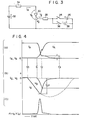
- Fig. 3 is a circuit diagram for explaining the operation of the GTO thyristor.
- a closed circuit consisting of an on-gate power source 26, a switch 24, a circuit impedance 28 and a GTO thyristor 30 has an on-gate current circulating therein.
- the GTO thyristor 30 is triggered by the on-gate current and rendered conductive. The result is that a main current flows in a closed circuit consisting of a main power source 32, a load 34, and the GTO thyristor 30, in other words, the anode current IA of the GTO thyristor 30.
- the switch 36 of an off-gate circuit is turned on. Then, a gate current ig having a direction opposite to that occurring when the GTO thyristor is gate turned on, flows in a closed circuit consisting of an off-gate power source 38, the switch 36, the circuit impedance 28, and the GTO thyristor 30. The gate current ig turns off the GTO thyristor 30.
- Figs. 4A, 4 B and 4C show waveforms for explaining the operation of the GTO thyristor 30 when it is gate turned off.
- the GTO thyristor 30 When the GTO thyristor 30 is conductive, if the gate turn-off switch 36 is closed at time t0, the off-gate current ig increases toward the negative (Fig. 4B). At time tl, the anode current IA starts to decrease and at the same time the voltage VA across the anode and the cathode also starts to increase (Fig. 4A).
- the junction between the gate and the cathode is restored, and the gate-cathode voltage vg reaches a negative maximum.
- the gate current ig reaches a negative maximum before the gate-cathode voltage vg reaches the negative peak value, and the gate current ig then sharply reduces toward the positive (Fig. 4B).
- the anode current IA has a current value based on the residual charge in the GTO thyristor.
- the current with an initial value It and flowing after time t2 is called a tail current (Fig. 4A).
- the anode current IA flowing after time t2 continues to flow until time t3 when the stored charge in the GTO thyristor disappears (Fig. 4A).
- Fig. 4B when the voltage EG of the off-gate power source 38 is lower than the gate-cathode reverse breakdown voltage V S1 of the GTO thyristor (EG ⁇ V S1 ), the gate current ig reaches its negative peak and decreases as indicated by a solid line.
- the gate current ig when the voltage EG of the off-gate power source 38 is larger than the gate-cathode breakdown voltage V J1 (EG > V J1 ), the gate current ig further increases toward the negative and than decreases as indicated by a broken line.
- the same relationship is illustrated with parameters A to D of an off-gate current rising rate (dig/dt).
- the parameters are in the order of A ⁇ B ⁇ C ⁇ D.
- Q G changes linearly with respect to IA and this is little influenced by the off-gate current rising rate (dig/dt). This implies that to turn off an anode current, a substantially constant off-gate charge quantity Q G is required irrespective of the rising rate of the off-gate current.
- Fig. 6 shows a relationship of the turn-off time toff with respect to an off-gate charge quantity discharged'per unit time when the anode current is constant. As seen from the graph, to shorten the turn-off time toff, the off-gate charge quantity Q G discharged per unit time must be increased.
- the circuit impedance 28 in the off-gate circuit has only a negligible amount of DC resistance, and a rising rate dig/dt ( ⁇ E G/ L) of the off-gate current is determined by the inductance L. Therefore, the off-gate charge Q G is given approximately as:
- an object of the present invention is to provide a gate turn-off thyristor with reduced power loss.
- Another object of the present invention is to provide a gate turn-off thyristor which may shorten a gate turn-off time without increasing the latching current and the forward voltage drop.
- a plurality of gate electrodes are provided on the second base layer.
- Each of the gate electrodes surrounds at least one cathode electrode.
- a current of Ik/m which is obtained by dividing the cathode current Ik by the number of the gate electrodes m, flows as the cathode current into each cathode electrode surrounded by a corresponding gate electrode.
- the cathode current Ik is substantially equal to the anode current IA, if the current Ik becomes smaller, the off-gate charge Q G also becomes smaller, as seen from Fig. 5. Accordingly, the equation (1) shows that if the gate turn-off time toff is equal to that of the prior thyristor, the off-gate voltage EG may be smaller. Further, by making the EG smaller, the tail current becomes smaller, so that the power loss P at the time of turn-off may be reduced. Further, with the smaller EG, the Zener current flowing after the turn off may be prevented, improving the reliability of the GTO thyristor.
- the gate turn-off time toff may be reduced, as seen from the equation (1).
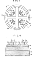
- the gate electrode 40 consists of four gate electrodes 40a, 40b, 40c and 40d.
- the number of the gate electrodes may properly be selected, for example, at more or less than 4.
- the GTO thyristor is equivalent to m number of thyristors each having 1/m volume of the GTO thyristor arranged in parallel.
- each cathode electrode surrounded by the corresponding gate electrode 40a, 40b, 40c or 40d is 1/4 of the cathode current of the whole thyristor.
- dig/dt E G/ L for each gate electrode 40a to 40d where the gate power source voltage is EG and the total inductance of the gate circuit is L.
- An off-gate charge quantity Q G per gate is also given, like the equation (1),
- the Q G pulled out by each gate electrode is smaller than that of the prior GTO not with a plurality of gate electrodes.
- the Eg when the same turn-off time toff as that of the prior GTO thyristor is employed, the Eg may be smaller than the prior one.
- the smaller Eg may lessen a probability that the Zener current flows after the turn off. This improves the reliability of the GTO thyristor.
- the toff may be made smaller. Therefore, unlike the prior art, there is no need for the heavy metal doping or the special structure. Therefore, the latching current and the forward voltage drop are never increased.
- the GTO thyristor with such a structure may be realized by the same fabricating process steps as those of the prior art. Specifically, the cathode electrodes 18 1 to 18n shown in Figs. 7 and 8 and the gate electrodes 40a to 40d are formed in a manner such that soft metal, e.g., aluminum is uniformly deposited over the main surfaces of the cathode and the gate of the semiconductor, and unnecessary soft metal portions are etched away using a resist mask having gate electrode patterns. Therefore, no additional cost is required for reducing the invention to practice.
- soft metal e.g., aluminum
- a sheet resistance of the second base layer 14 is normally several tens n/0, and hence the gate electrodes are electrically separated to a satisfactory extent, thus attaining the effect by this invention.
- the present invention is not limited to the above-mentioned embodiment any way.
- the present invention is applicable for the GTO thyristor with a structure such that a part of the first base layer is exposed to the main surface of the anode surface and the first emitter layer and the first base layer are shorted by the anode electrode.
Landscapes
- Thyristors (AREA)
Applications Claiming Priority (2)
| Application Number | Priority Date | Filing Date | Title |
|---|---|---|---|
| JP56169889A JPS5871657A (ja) | 1981-10-23 | 1981-10-23 | ゲ−トタ−ンオフサイリスタ |
| JP169889/81 | 1981-10-23 |
Publications (3)
| Publication Number | Publication Date |
|---|---|
| EP0077930A2 true EP0077930A2 (fr) | 1983-05-04 |
| EP0077930A3 EP0077930A3 (en) | 1984-10-24 |
| EP0077930B1 EP0077930B1 (fr) | 1987-05-06 |
Family
ID=15894831
Family Applications (1)
| Application Number | Title | Priority Date | Filing Date |
|---|---|---|---|
| EP82108973A Expired EP0077930B1 (fr) | 1981-10-23 | 1982-09-28 | Thyristor à blocage par la gâchette |
Country Status (3)
| Country | Link |
|---|---|
| EP (1) | EP0077930B1 (fr) |
| JP (1) | JPS5871657A (fr) |
| DE (1) | DE3276286D1 (fr) |
Cited By (5)
| Publication number | Priority date | Publication date | Assignee | Title |
|---|---|---|---|---|
| US4559697A (en) * | 1984-02-23 | 1985-12-24 | Mitsubishi Denki Kabushiki Kaisha | Method of fixing insertion electrode panel in compression-bonded semiconductor device |
| EP0220469A1 (fr) * | 1985-10-15 | 1987-05-06 | Siemens Aktiengesellschaft | Thyristor de puissance |
| EP0146928A3 (en) * | 1983-12-21 | 1987-08-26 | Kabushiki Kaisha Toshiba | Power semiconductor device with mesa type structure |
| DE3723150A1 (de) * | 1986-07-14 | 1988-01-21 | Hitachi Ltd | Gto-thyristor |
| US4929856A (en) * | 1988-01-26 | 1990-05-29 | Asea Brown Boveri Ag | Heavy-duty circuit breaker |
Family Cites Families (8)
| Publication number | Priority date | Publication date | Assignee | Title |
|---|---|---|---|---|
| BE755356A (fr) * | 1969-08-27 | 1971-03-01 | Westinghouse Electric Corp | Interrupteur a semi conducteur a grille de commande pour courant eleve |
| JPS513384A (en) * | 1974-06-28 | 1976-01-12 | Yamato Shokaki Kk | Hatsuhoseinoshukueki |
| US4127863A (en) * | 1975-10-01 | 1978-11-28 | Tokyo Shibaura Electric Co., Ltd. | Gate turn-off type thyristor with separate semiconductor resistive wafer providing emitter ballast |
| JPS6040190B2 (ja) * | 1976-07-21 | 1985-09-10 | 日本インタ−ナシヨナル整流器株式会社 | 半導体制御整流素子 |
| FR2377095A1 (fr) * | 1977-01-10 | 1978-08-04 | Alsthom Atlantique | Thyristor a amplificateur de declenchement et a ouverture commandee par la gachette |
| JPS54136186A (en) * | 1978-04-14 | 1979-10-23 | Hitachi Ltd | Semiconductor device |
| JPS6019147B2 (ja) * | 1979-01-24 | 1985-05-14 | 株式会社日立製作所 | ゲ−ト・タ−ン・オフ・サイリスタ |
| JPS6043668B2 (ja) * | 1979-07-06 | 1985-09-30 | 株式会社日立製作所 | 半導体装置 |
-
1981
- 1981-10-23 JP JP56169889A patent/JPS5871657A/ja active Pending
-
1982
- 1982-09-28 DE DE8282108973T patent/DE3276286D1/de not_active Expired
- 1982-09-28 EP EP82108973A patent/EP0077930B1/fr not_active Expired
Cited By (7)
| Publication number | Priority date | Publication date | Assignee | Title |
|---|---|---|---|---|
| EP0146928A3 (en) * | 1983-12-21 | 1987-08-26 | Kabushiki Kaisha Toshiba | Power semiconductor device with mesa type structure |
| US4559697A (en) * | 1984-02-23 | 1985-12-24 | Mitsubishi Denki Kabushiki Kaisha | Method of fixing insertion electrode panel in compression-bonded semiconductor device |
| EP0220469A1 (fr) * | 1985-10-15 | 1987-05-06 | Siemens Aktiengesellschaft | Thyristor de puissance |
| US4868636A (en) * | 1985-10-15 | 1989-09-19 | Siemens Aktiengesellschaft | Power thyristor |
| DE3723150A1 (de) * | 1986-07-14 | 1988-01-21 | Hitachi Ltd | Gto-thyristor |
| US5021855A (en) * | 1986-07-14 | 1991-06-04 | Hitachi, Ltd. | Gate turn-off thyristor |
| US4929856A (en) * | 1988-01-26 | 1990-05-29 | Asea Brown Boveri Ag | Heavy-duty circuit breaker |
Also Published As
| Publication number | Publication date |
|---|---|
| EP0077930B1 (fr) | 1987-05-06 |
| DE3276286D1 (en) | 1987-06-11 |
| JPS5871657A (ja) | 1983-04-28 |
| EP0077930A3 (en) | 1984-10-24 |
Similar Documents
| Publication | Publication Date | Title |
|---|---|---|
| EP0794578B1 (fr) | Diode et appareil convertisseur de puissance | |
| EP0022355B1 (fr) | Thyristor à blocage par la gâchette | |
| EP0154082B1 (fr) | Thyristor à blocage par la gâchette | |
| US5747841A (en) | Circuit arrangement, and junction field effect transistor suitable for use in such a circuit arrangement | |
| US5463344A (en) | Fast turn on switch circuit with parallel MOS controlled thyristor and silicon controlled rectifier | |
| US3526815A (en) | Controllable semi-conductor devices comprising main and auxiliary thyristors having all except one emitter-layer in common | |
| US3622845A (en) | Scr with amplified emitter gate | |
| US5144400A (en) | Power semiconductor device with switch-off facility | |
| JPH11274482A (ja) | 半導体装置 | |
| US6664591B2 (en) | Insulated gate semiconductor device | |
| EP0064231A2 (fr) | Dispositif semiconducteur à compression | |
| EP0077930A2 (fr) | Thyristor à blocage par la gâchette | |
| US4315274A (en) | Thyristor with switchable capacitor between auxiliary thyristor cathode and main thyristor gate regions | |
| US3474303A (en) | Semiconductor element having separated cathode zones | |
| US3409811A (en) | Four-zone semiconductor rectifier with spaced regions in one outer zone | |
| JP2687163B2 (ja) | ターンオフ可能なサイリスタ | |
| US4581626A (en) | Thyristor cathode and transistor emitter structures with insulator islands | |
| US4063277A (en) | Semiconductor thyristor devices having breakover protection | |
| EP0128268B1 (fr) | Dispositif à semi-conducteur ayant une électrode de commande | |
| US3836994A (en) | Thyristor overvoltage protective element | |
| JP2001223354A (ja) | 逆導通機能を有する半導体装置 | |
| JPS6248392B2 (fr) | ||
| US5017992A (en) | High blocking-capacity semiconductor component | |
| US4825270A (en) | Gate turn-off thyristor | |
| US5010384A (en) | Gate turn-off thyristor with resistance layers |
Legal Events
| Date | Code | Title | Description |
|---|---|---|---|
| PUAI | Public reference made under article 153(3) epc to a published international application that has entered the european phase |
Free format text: ORIGINAL CODE: 0009012 |
|
| 17P | Request for examination filed |
Effective date: 19820928 |
|
| AK | Designated contracting states |
Designated state(s): DE FR GB SE |
|
| PUAL | Search report despatched |
Free format text: ORIGINAL CODE: 0009013 |
|
| RAP1 | Party data changed (applicant data changed or rights of an application transferred) |
Owner name: KABUSHIKI KAISHA TOSHIBA |
|
| AK | Designated contracting states |
Designated state(s): DE FR GB SE |
|
| 17Q | First examination report despatched |
Effective date: 19860206 |
|
| GRAA | (expected) grant |
Free format text: ORIGINAL CODE: 0009210 |
|
| AK | Designated contracting states |
Kind code of ref document: B1 Designated state(s): DE SE |
|
| REF | Corresponds to: |
Ref document number: 3276286 Country of ref document: DE Date of ref document: 19870611 |
|
| PLBE | No opposition filed within time limit |
Free format text: ORIGINAL CODE: 0009261 |
|
| STAA | Information on the status of an ep patent application or granted ep patent |
Free format text: STATUS: NO OPPOSITION FILED WITHIN TIME LIMIT |
|
| 26N | No opposition filed | ||
| PGFP | Annual fee paid to national office [announced via postgrant information from national office to epo] |
Ref country code: SE Payment date: 19930917 Year of fee payment: 12 |
|
| PGFP | Annual fee paid to national office [announced via postgrant information from national office to epo] |
Ref country code: DE Payment date: 19930922 Year of fee payment: 12 |
|
| PG25 | Lapsed in a contracting state [announced via postgrant information from national office to epo] |
Ref country code: SE Effective date: 19940929 |
|
| EAL | Se: european patent in force in sweden |
Ref document number: 82108973.7 |
|
| PG25 | Lapsed in a contracting state [announced via postgrant information from national office to epo] |
Ref country code: DE Effective date: 19950601 |
|
| EUG | Se: european patent has lapsed |
Ref document number: 82108973.7 |