EP0078117A2 - Circuit onduleur - Google Patents
Circuit onduleur Download PDFInfo
- Publication number
- EP0078117A2 EP0078117A2 EP82305332A EP82305332A EP0078117A2 EP 0078117 A2 EP0078117 A2 EP 0078117A2 EP 82305332 A EP82305332 A EP 82305332A EP 82305332 A EP82305332 A EP 82305332A EP 0078117 A2 EP0078117 A2 EP 0078117A2
- Authority
- EP
- European Patent Office
- Prior art keywords
- capacitor
- diodes
- voltage
- inverter
- switching means
- Prior art date
- Legal status (The legal status is an assumption and is not a legal conclusion. Google has not performed a legal analysis and makes no representation as to the accuracy of the status listed.)
- Granted
Links
Images
Classifications
-
- H—ELECTRICITY
- H02—GENERATION; CONVERSION OR DISTRIBUTION OF ELECTRIC POWER
- H02M—APPARATUS FOR CONVERSION BETWEEN AC AND AC, BETWEEN AC AND DC, OR BETWEEN DC AND DC, AND FOR USE WITH MAINS OR SIMILAR POWER SUPPLY SYSTEMS; CONVERSION OF DC OR AC INPUT POWER INTO SURGE OUTPUT POWER; CONTROL OR REGULATION THEREOF
- H02M7/00—Conversion of AC power input into DC power output; Conversion of DC power input into AC power output
- H02M7/42—Conversion of DC power input into AC power output without possibility of reversal
- H02M7/44—Conversion of DC power input into AC power output without possibility of reversal by static converters
- H02M7/48—Conversion of DC power input into AC power output without possibility of reversal by static converters using discharge tubes with control electrode or semiconductor devices with control electrode
- H02M7/53—Conversion of DC power input into AC power output without possibility of reversal by static converters using discharge tubes with control electrode or semiconductor devices with control electrode using devices of a triode or transistor type requiring continuous application of a control signal
- H02M7/537—Conversion of DC power input into AC power output without possibility of reversal by static converters using discharge tubes with control electrode or semiconductor devices with control electrode using devices of a triode or transistor type requiring continuous application of a control signal using semiconductor devices only, e.g. single switched pulse inverters
-
- H—ELECTRICITY
- H02—GENERATION; CONVERSION OR DISTRIBUTION OF ELECTRIC POWER
- H02M—APPARATUS FOR CONVERSION BETWEEN AC AND AC, BETWEEN AC AND DC, OR BETWEEN DC AND DC, AND FOR USE WITH MAINS OR SIMILAR POWER SUPPLY SYSTEMS; CONVERSION OF DC OR AC INPUT POWER INTO SURGE OUTPUT POWER; CONTROL OR REGULATION THEREOF
- H02M5/00—Conversion of AC power input into AC power output, e.g. for change of voltage, for change of frequency, for change of number of phases
- H02M5/40—Conversion of AC power input into AC power output, e.g. for change of voltage, for change of frequency, for change of number of phases with intermediate conversion into DC
- H02M5/42—Conversion of AC power input into AC power output, e.g. for change of voltage, for change of frequency, for change of number of phases with intermediate conversion into DC by static converters
- H02M5/44—Conversion of AC power input into AC power output, e.g. for change of voltage, for change of frequency, for change of number of phases with intermediate conversion into DC by static converters using discharge tubes or semiconductor devices to convert the intermediate DC into AC
- H02M5/453—Conversion of AC power input into AC power output, e.g. for change of voltage, for change of frequency, for change of number of phases with intermediate conversion into DC by static converters using discharge tubes or semiconductor devices to convert the intermediate DC into AC using devices of a triode or transistor type requiring continuous application of a control signal
- H02M5/458—Conversion of AC power input into AC power output, e.g. for change of voltage, for change of frequency, for change of number of phases with intermediate conversion into DC by static converters using discharge tubes or semiconductor devices to convert the intermediate DC into AC using devices of a triode or transistor type requiring continuous application of a control signal using semiconductor devices only
Definitions
- This invention relates to an inverter circuit /particularly but not exclusively, /to improvements in an inverter circuit for driving an AC motor.
- inverter It has become possible to control the speed of recently developed AC motors in simple fashion by varying the frequency of an alternating current delivered from the output side of an may be inverter.
- the type of inverter involved / composed of switching elements such as a plurality of transistors or thyristors connected in the form of a bridge, and converts a direct current applied to its input side into an alternating current owing to the switching action of the switching elements.
- the switching elements in the inverter produce sharp electrical spikes which are a source of noise and . reduce or which may even damage the elements.
- a so-called snubber circuit comprising a capacitor, resistor and diode in parallel is connected across both ends of each switching element so that the spikes produced by the switching elements may be absorbed within the snubber circuits.
- Such an arrangement is disadvantageous, however, in that providing each switching element with a snubber circuit complicates the overall proposed circuitry.
- An improvement has been /to employ circuitry wherein a capacitor of large capacitance is connected to the inverter input circuit for the purpose of absorbing spikes produced by the inverter.
- a contactor may be provided on the inverter input side.
- a large momentary current flows into the spike absorbing capacitor from the source of direct current, requiring that the source, such as a rectifying circuit, be large enough in size to withstand the large momentary current. This is a requirement that, because of cost, results in poor economy.
- Another shortcoming is that a large rush current flows into the spike absorbing capacitor, thereby shortening its life, each time the machine tool is actuated.
- an inverter circuit having a bridge circuit composed of a plurality of switching elements connected in the form of a bridge for converting, into alternating current, a DC.voltage which is produced by a DC voltage generating unit and which is received through first switching means, said inverter circuit comprising a pair of diodes and a spike absorbing capacitor, said diodes and spike absorbing capacitor constituting a series network wherein said diodes are connected so as to be forward biased with respect to the DC voltage and said spike absorbing capacitor is connected between said diodes, said series network being connected in parallel with said bridge circuit across the input terminals thereof and having both ends thereof connected to the DC voltage generating unit through said first switching means, said spike absorbing capacitor being connected to a DC charging means operable to precharge the spike absorbing capacitor prior to said DC voltage being applied to the bridge circuit.
- An embodiment of the present invention may provide an inverter circuit wherein it is possible to absorb the spikes that are produced during the on/off switching action of the switching elements such as transistors or thyristors constituting the inverter.
- An embodiment of the present invention may provide an inverter circuit so designed that a large rush current will not flow into a spike absorbing capacitor or into the diodes constituting a rectifying circuit whenever a DC voltage is impressed upon the inverter by the action of a contactor.
- An embodiment of the present invention may provide an inverter circuit in which it is unnecessary to employ diodes of large size for constructing a rectifying circuit.
- An embodiment of the present invention may provide an inverter circuit which, through a simple circuit arrangement, makes it possible to absorb spikes without causing large rush currents to flow.
- spike pulses produced by the switching elements constituting the inverter are completely or at least partially absorbed by the capacitor through the diodes.
- the spike absorbing capacitor may be constantly charged by connection to a source of DC current, so that large rush currents do not flow into the capacitor whenever a voltage is impressed upon the inverter.
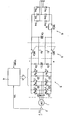
- the Figure shows an operational control device for controlling the speed of an AC motor, specifically a three-phase induction motor, through the use of an inverter.
- Numeral 1 denotes a three-phase induction motor, the rotational.speed whereof is sensed by a tachogenerator 2.
- the induction motor 1 is driven by an inverter 3, including six bridge-connected transistors TR1 through TR6, to the output side of which the induction motor 1 is connected as a load.
- the inverter 3 also includes freewheel diodes ID.
- a diode Dl, a spike absorbing capacitor Cl and a diode D2 are serially connected, in the order mentioned, across the DC input terminals to the inverter 3.
- a speed control circuit 4 is provided and, though not shown, includes circuitry for controlling the switching of transistors TR1 through TR6 in the inverter 3 in accordance with a deviation between a commanded speed and the actual speed of the motor l.
- the speed control circuit 4 controls the switching of the transistors TR1 through TR6 on the basis of an externally applied speed command signal VCMD, whereby the inverter 3 produces a three-phase alternating current, of a prescribed effective voltage and frequency, which is impressed upon the three-phase induction motor 1 to rotate the motor.
- the tachogenerator 2 As the motor rotates, the tachogenerator 2 generates a voltage VR which conforms to the actual rotational speed of the motor.
- the speed control circuit 4 controls the on/off switching action of the transistors TR1 through TR6 so as to bring the actual motor speed into agreement with the commanded speed.
- An example of the speed control circuit 4 is disclosed in the specification of U.S.P. 4,327,315.
- Numeral 5 denotes a contactor portion having two contactors MC1, MC2 opened or closed simultaneously for cutting off the DC voltage from or applying it to the inverter 3, respectively.
- the three-phase induction motor 1 is being employed as the spindle motor of a machine tool.
- three-phase alternating current from the three-phase AC source R, S, T flows into the bridge circuit constituting the rectifying circuit 6, which proceeds to produce a DC voltage that appears on its output side.
- the contactor MC3 will initially be open, the direct current slowly charges the capacitors Cl, C2 through the resistor R.
- Contactor MC3 is closed at the point that the capacitors Cl and C2 become fully charged. When this occurs, the three-phase induction motor 1 is ready to operate.
- the first step is to provide the speed control circuit 4 with a speed command signal VCMD of the desired analog value, so that the control circuit 4 may produce control signals for controlling the transistors TRl through T R6 that constitute the inverter 3.
- the contactors MCl, MC2 are closed simultaneously. This applies the.direct current from the rectifying circuit 6 to the inverter 3, but since the capacitor Cl is already storing a charge, no rush current flows into the capacitor Cl through the diodes Dl; D2.
- the inverter 3 Upon receiving the direct current, the inverter 3 produces three-phase alternating current of a predetermined frequency from its outputs U, V, W, the current being applied to the three-phase induction motor 1 to drive the motor into rotation.
- the rotational speed of the motor is sensed by the tachogenerator 2, which responds by applying the voltage VR, indicative of actual rotational speed, to the speed control circuit 4.
- the latter responds by regulating the control signals applied to the inverter 3 in such a manner that the rotational speed of the motor 1 is made to approach the rotational speed specified by the speed command signal VCMD. Since electrical spike pulses generated when the transistors TR1 through TR6 turn on or off are absorbed by the capacitor Cl through the diodes Dl, D2, the spikes do not leak out toward the three-phase AC power source R, S, T through the contactor portion 5 and rectifying circuit 6.
- the first step is to set the speed command signal VCMD to zero, so that the speed control circuit 4 will issue control signals for decelerating and finally stopping the motor.
- Contactors MC1, MC2 of the contactor portion 5 are opened after the motor 1 stops. Note that capacitor Cl still receives voltage from the rectifying circuit 6, and therefore remains charged, even when the contactor portion 5 is opened. Since the diodes Dl, D2 become reversely biased, moreover, the inverter 3 is isolated from the rectifying circuit 6.
- capacitor Cl While it is preferred that the voltage charged in capacitor Cl be approximately equivalent to the DC voltage impressed upon the inverter 3, a somewhat lower voltage is sufficient. It also does not matter whether the capacitor Cl is charged by the rectifying circuit 6, as in the preferred embodiment, or by another suitably arranged circuit.
- the diodes Dl, D2 are connected across the input terminals to the inverter 3 in such fashion as to be forward biased with respect to the power source, and the spike absorbing capacitor Cl is inserted between the diodes Dl, D2 and connected in series therewith.
- the spike absorbing capacitor Cl is inserted between the diodes Dl, D2 and connected in series therewith.
Landscapes
- Engineering & Computer Science (AREA)
- Power Engineering (AREA)
- Inverter Devices (AREA)
- Power Conversion In General (AREA)
Applications Claiming Priority (2)
| Application Number | Priority Date | Filing Date | Title |
|---|---|---|---|
| JP56161239A JPS5863082A (ja) | 1981-10-09 | 1981-10-09 | インバータ装置 |
| JP161239/81 | 1981-10-09 |
Publications (3)
| Publication Number | Publication Date |
|---|---|
| EP0078117A2 true EP0078117A2 (fr) | 1983-05-04 |
| EP0078117A3 EP0078117A3 (en) | 1983-12-07 |
| EP0078117B1 EP0078117B1 (fr) | 1986-03-05 |
Family
ID=15731282
Family Applications (1)
| Application Number | Title | Priority Date | Filing Date |
|---|---|---|---|
| EP82305332A Expired EP0078117B1 (fr) | 1981-10-09 | 1982-10-07 | Circuit onduleur |
Country Status (4)
| Country | Link |
|---|---|
| US (1) | US4482854A (fr) |
| EP (1) | EP0078117B1 (fr) |
| JP (1) | JPS5863082A (fr) |
| DE (1) | DE3269662D1 (fr) |
Cited By (1)
| Publication number | Priority date | Publication date | Assignee | Title |
|---|---|---|---|---|
| DE102008007658A1 (de) * | 2008-02-06 | 2009-08-13 | Siemens Aktiengesellschaft | Statischer Umformer |
Families Citing this family (12)
| Publication number | Priority date | Publication date | Assignee | Title |
|---|---|---|---|---|
| JPS59165970A (ja) * | 1983-03-11 | 1984-09-19 | Meidensha Electric Mfg Co Ltd | 電流形gtoインバ−タの電圧クランプ回路 |
| WO1987003928A1 (fr) * | 1985-12-23 | 1987-07-02 | Sundstrand Corporation | Convertisseur de puissance pour un entrainement a vitesse constante compense electriquement |
| US4695776A (en) * | 1985-12-23 | 1987-09-22 | Sunstrand Corporation | Power converter for an electrically-compensated constant speed drive |
| IN172421B (fr) * | 1989-03-14 | 1993-07-24 | Kone Elevator Gmbh | |
| JP3196416B2 (ja) * | 1993-04-21 | 2001-08-06 | 松下電器産業株式会社 | 自動車用空調装置 |
| JP3191481B2 (ja) * | 1993-04-21 | 2001-07-23 | 松下電器産業株式会社 | 自動車用空調装置 |
| JP3734236B2 (ja) * | 1997-12-10 | 2006-01-11 | サンデン株式会社 | 電気自動車用空調装置の電源入力回路 |
| EP2113999A3 (fr) * | 2001-09-25 | 2010-01-06 | Daikin Industries, Ltd. | Appareil de détection de courant de phase |
| FR2928058B1 (fr) * | 2008-02-21 | 2010-02-19 | Schneider Toshiba Inverter | Variateur de vitesse incluant un dispositif de protection contre les surintensites et les surtensions. |
| JP2013069859A (ja) * | 2011-09-22 | 2013-04-18 | Toshiba Corp | 半導体装置 |
| US8724266B2 (en) * | 2012-08-02 | 2014-05-13 | Renewable Power Conversion, Inc. | Photovoltaic switchgear with sacrificial fuse |
| US10050572B2 (en) | 2014-12-19 | 2018-08-14 | Black & Decker Inc. | Power tool with electric motor and auxiliary switch path |
Family Cites Families (11)
| Publication number | Priority date | Publication date | Assignee | Title |
|---|---|---|---|---|
| AT224738B (de) * | 1959-04-02 | 1962-12-10 | Int Standard Electric Corp | Schutzschaltung für Silizium-Gleichrichter |
| US3047746A (en) * | 1959-12-08 | 1962-07-31 | Bell Telephone Labor Inc | Surge suppression for power supplies |
| DE1956145C3 (de) * | 1969-11-07 | 1978-06-15 | Siemens Ag | Schaltungsanordnung zum Schutz von induktiv belasteten Schalttransistoren gegen Überspannungen |
| US3793535A (en) * | 1972-12-06 | 1974-02-19 | Gen Electric | Circuit for protecting semiconductors against transient voltages |
| DE2451578A1 (de) * | 1974-10-30 | 1976-05-13 | Siemens Ag | Schaltung zur ueberspannungsbegrenzung in gleichstrom-verteilsystemen |
| JPS5154224A (fr) * | 1974-11-08 | 1976-05-13 | Hitachi Ltd | |
| JPS5271654A (en) * | 1975-12-12 | 1977-06-15 | Hitachi Ltd | Over-voltage protector for inverter |
| US4095163A (en) * | 1976-06-01 | 1978-06-13 | Control Concepts Corporation | Transient voltage suppression circuit |
| SU718876A1 (ru) * | 1976-09-20 | 1980-02-29 | Рижский Ордена Трудового Красного Знамени Политехнический Институт | Сглаживающий фильтр мостового выпр мител |
| JPS5931286B2 (ja) * | 1978-10-11 | 1984-08-01 | 関西電力株式会社 | 系統連系方法 |
| US4327405A (en) * | 1980-05-16 | 1982-04-27 | Sperry Corporation | Voltage suppression circuit for a DC-to-DC voltage converter circuit |
-
1981
- 1981-10-09 JP JP56161239A patent/JPS5863082A/ja active Granted
-
1982
- 1982-10-06 US US06/433,103 patent/US4482854A/en not_active Expired - Fee Related
- 1982-10-07 EP EP82305332A patent/EP0078117B1/fr not_active Expired
- 1982-10-07 DE DE8282305332T patent/DE3269662D1/de not_active Expired
Cited By (2)
| Publication number | Priority date | Publication date | Assignee | Title |
|---|---|---|---|---|
| DE102008007658A1 (de) * | 2008-02-06 | 2009-08-13 | Siemens Aktiengesellschaft | Statischer Umformer |
| US8054657B2 (en) | 2008-02-06 | 2011-11-08 | Siemens Aktiengesellschaft | Static converter |
Also Published As
| Publication number | Publication date |
|---|---|
| JPH0363313B2 (fr) | 1991-09-30 |
| JPS5863082A (ja) | 1983-04-14 |
| US4482854A (en) | 1984-11-13 |
| EP0078117A3 (en) | 1983-12-07 |
| EP0078117B1 (fr) | 1986-03-05 |
| DE3269662D1 (en) | 1986-04-10 |
Similar Documents
| Publication | Publication Date | Title |
|---|---|---|
| US4959602A (en) | Ac motor drive with improved voltage-source inverter | |
| AU589803B2 (en) | Alternating current motor control apparatus | |
| EP0078117B1 (fr) | Circuit onduleur | |
| US4573113A (en) | Surge protection system for a d-c power supply during power-up | |
| US4375612A (en) | Controlled regenerative d-c power supply | |
| JPS62107647A (ja) | フライホイ−ル電源装置 | |
| JPH0575669B2 (fr) | ||
| JPH06105405A (ja) | 電気自動車の制動制御装置 | |
| JPH0348754B2 (fr) | ||
| EP0026038B1 (fr) | Dispositif pour contrôler la marche de moteurs à courant alternatif | |
| GB2203301A (en) | Soft-start rectifier circuit | |
| US3866098A (en) | Electrical motor drive system with field control operable in motoring and braking modes | |
| JPH0340787A (ja) | 電動機の制御装置 | |
| JP2976714B2 (ja) | モータ駆動装置 | |
| JPH07289766A (ja) | 工業用ミシン駆動装置 | |
| US4415846A (en) | Wound rotor motor apparatus | |
| JPH06225458A (ja) | 電力変換装置及び制御方法 | |
| JPS6322156B2 (fr) | ||
| GB2059192A (en) | Controlled regenerative D-C power supply | |
| JPH0669316B2 (ja) | 電力変換装置の電力回生制御回路 | |
| JPH0127436Y2 (fr) | ||
| KR830002573Y1 (ko) | 제어 재생식 직류전원 | |
| JPS59165987A (ja) | 誘導電動機制御装置 | |
| JPH0746073Y2 (ja) | 電力変換器 | |
| KR920006435Y1 (ko) | 전력변환회로 |
Legal Events
| Date | Code | Title | Description |
|---|---|---|---|
| PUAI | Public reference made under article 153(3) epc to a published international application that has entered the european phase |
Free format text: ORIGINAL CODE: 0009012 |
|
| AK | Designated contracting states |
Designated state(s): DE FR GB |
|
| PUAL | Search report despatched |
Free format text: ORIGINAL CODE: 0009013 |
|
| RHK1 | Main classification (correction) |
Ipc: H02M 1/14 |
|
| AK | Designated contracting states |
Designated state(s): DE FR GB |
|
| 17P | Request for examination filed |
Effective date: 19840522 |
|
| GRAA | (expected) grant |
Free format text: ORIGINAL CODE: 0009210 |
|
| AK | Designated contracting states |
Kind code of ref document: B1 Designated state(s): DE FR GB |
|
| REF | Corresponds to: |
Ref document number: 3269662 Country of ref document: DE Date of ref document: 19860410 |
|
| ET | Fr: translation filed | ||
| PLBE | No opposition filed within time limit |
Free format text: ORIGINAL CODE: 0009261 |
|
| STAA | Information on the status of an ep patent application or granted ep patent |
Free format text: STATUS: NO OPPOSITION FILED WITHIN TIME LIMIT |
|
| 26N | No opposition filed | ||
| PGFP | Annual fee paid to national office [announced via postgrant information from national office to epo] |
Ref country code: FR Payment date: 19910918 Year of fee payment: 10 |
|
| PGFP | Annual fee paid to national office [announced via postgrant information from national office to epo] |
Ref country code: GB Payment date: 19910924 Year of fee payment: 10 |
|
| PG25 | Lapsed in a contracting state [announced via postgrant information from national office to epo] |
Ref country code: GB Effective date: 19921007 |
|
| GBPC | Gb: european patent ceased through non-payment of renewal fee |
Effective date: 19921007 |
|
| PG25 | Lapsed in a contracting state [announced via postgrant information from national office to epo] |
Ref country code: FR Effective date: 19930630 |
|
| REG | Reference to a national code |
Ref country code: FR Ref legal event code: ST |
|
| PGFP | Annual fee paid to national office [announced via postgrant information from national office to epo] |
Ref country code: DE Payment date: 19931011 Year of fee payment: 12 |
|
| PG25 | Lapsed in a contracting state [announced via postgrant information from national office to epo] |
Ref country code: DE Effective date: 19950701 |