EP0078687A2 - Analog-Digital-Wandler - Google Patents
Analog-Digital-Wandler Download PDFInfo
- Publication number
- EP0078687A2 EP0078687A2 EP82305778A EP82305778A EP0078687A2 EP 0078687 A2 EP0078687 A2 EP 0078687A2 EP 82305778 A EP82305778 A EP 82305778A EP 82305778 A EP82305778 A EP 82305778A EP 0078687 A2 EP0078687 A2 EP 0078687A2
- Authority
- EP
- European Patent Office
- Prior art keywords
- converter
- analog
- digital
- signal
- bits
- Prior art date
- Legal status (The legal status is an assumption and is not a legal conclusion. Google has not performed a legal analysis and makes no representation as to the accuracy of the status listed.)
- Granted
Links
Images
Classifications
-
- H—ELECTRICITY
- H03—ELECTRONIC CIRCUITRY
- H03M—CODING; DECODING; CODE CONVERSION IN GENERAL
- H03M1/00—Analogue/digital conversion; Digital/analogue conversion
- H03M1/12—Analogue/digital converters
- H03M1/34—Analogue value compared with reference values
- H03M1/38—Analogue value compared with reference values sequentially only, e.g. successive approximation type
Definitions
- the present invention relates generally to an analog to digital converter.
- A/D analog to digital
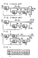
- the prior art A/D converter shown in Figure 1 is used to carry out 8-bit A/D conversion.
- an analog input voltage V in is applied to an A/D converter 1 of, for example, 3-bits from which digital outputs D 7 to D 5 constituting the upper 3 bits of the resulting digital word are obtained.
- These 3-bit digital output D 7 to D 5 are supplied to a digital to analog (hereinbelow referred simply to as D/A) converter 2 and then converted thereby to an analog voltage V m .
- This difference voltage V s is applied to a 5 bit A/D converter 4 from which digital outputs D 4 to D 0 constituting the lower 5 bits of the digital word are derived.
- the digital outputs D 7 to D 5 and those D 4 to D 0 are delivered through a latch 5 as an A/D converted output of 8 bits.
- the upper bit converter 1 needs to have an accuracy the same as that of the lower bit converter 4. The reason is as follows.
- a converter such as that shown in Figure 2 which compensates for the accuracy of the converter 1.
- the converter 4 is provided with a redundant bit so as to be 6-bits, and 6-bit outputs D 5 to D 0 therefrom and the outputs D 7 to D 5 from the converter 1 are added in an adding circuit 6 so as to make the D 5 bits coincident with each other.
- an analog to digital converter comprising: a first analog to digital converter for converting a first analog signal to a first digital signal; a code converter for converting said first digital signal to a second digital signal; a digital to analog converter for converting said second digital signal to a second analog signal; a subtractor for subtracting said second analog signal from said first analog signal; a second analog to digital converter for converting an output signal of said subtractor to a third digital signal; and an adder for adding said second digital signal and said third digital signal.
- the analog input voltage V in is applied to an A/D converter 11 of, for example, 3-bits to be thereby converted to a digital value Q 11 of 3-bits.
- the conversion accuracy (scattering upon conversion) of the converter 11 is within +2 LSB (least significant bit) of the final digital outputs D 7 to DO and the value "28" of the lower 5 bits D 4 to D 0 is taken as to correspond to "1" of the signal Q 11 .
- the signal Q11 is supplied to a code-converter 17 formed of, for example, a ROM (read only memory) and then converted to a digital value Q 17 (which is 8 bits) 28 times the value Q11 as shown in Figure 4.
- This signal Q17 is supplied to a D/A converter 12 and then converted to an analog voltage V 12 .
- the voltage V 13 is applied to an A/D converter 14 of, for example, 5-bits and converted to a digital value Q 14 of 5-bits.
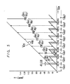
- the output signal Q 16 is as follows:
- this signal Q 16 is the A/D converted output of the input voltage V in .
- the output signal Q 11 from the A/D converter 11 always includes the scattering of + 2 LSB so that for the signal Q 11 to be shifted to the preceding or succeeding value completely, a width of 4 LSB is required. If the input voltage V in exists within this width or an interval of 4 LSB, it is uncertain whether the value of the signal Q11 becomes the preceding or succeeding value.
- the output signal is not affected thereby. Further, the redundant bit required in the prior art A/D converter shown in Figure 2 is unnecessary in the A/D converter of this invention, so that the A/D converter has excellent efficiency.
- the dynamic range becomes as follows; under the condition that there is existing an uncertainty of width + 2 LSB at the step-difference portions.
- T is equivalent to the multiplication factor of code converter (17).
- the multiplication factor of the code converter (17) is expressed as T
- T is given by subtracting the width of the 4 LSB uncertanty from the total number of steps 32 in the second analog to digital converter. From the above reason, the value of T is not arbitrary, but must be determined on basis of the number of bits in the first and second analog to digital converters and the uncertainty widths of the first analog to digital converter. This means that if the product T is selected it will be possible to operate the present analog to digital converter efficiently and exactly. Thus, the dynamic range of the converter becomes narrower than the maximum of 256 steps for 8-bits.
- the luminance signal is A/D converted
- a further narrower dynamic range is enough.
- the above 228 steps are sufficient. If, however, 256 steps are required, it is sufficient that an A/D converter having an over-range output is used as the A/D converter 11.
Landscapes
- Engineering & Computer Science (AREA)
- Theoretical Computer Science (AREA)
- Analogue/Digital Conversion (AREA)
- Control Of Motors That Do Not Use Commutators (AREA)
Priority Applications (1)
| Application Number | Priority Date | Filing Date | Title |
|---|---|---|---|
| AT82305778T ATE30286T1 (de) | 1981-10-30 | 1982-10-29 | Analog-digital-wandler. |
Applications Claiming Priority (2)
| Application Number | Priority Date | Filing Date | Title |
|---|---|---|---|
| JP56174167A JPS5875920A (ja) | 1981-10-30 | 1981-10-30 | A/dコンバ−タ回路 |
| JP174167/81 | 1981-10-30 |
Publications (3)
| Publication Number | Publication Date |
|---|---|
| EP0078687A2 true EP0078687A2 (de) | 1983-05-11 |
| EP0078687A3 EP0078687A3 (en) | 1984-08-01 |
| EP0078687B1 EP0078687B1 (de) | 1987-10-14 |
Family
ID=15973871
Family Applications (1)
| Application Number | Title | Priority Date | Filing Date |
|---|---|---|---|
| EP82305778A Expired EP0078687B1 (de) | 1981-10-30 | 1982-10-29 | Analog-Digital-Wandler |
Country Status (7)
| Country | Link |
|---|---|
| US (1) | US4559523A (de) |
| EP (1) | EP0078687B1 (de) |
| JP (1) | JPS5875920A (de) |
| AT (1) | ATE30286T1 (de) |
| AU (1) | AU563148B2 (de) |
| CA (1) | CA1222826A (de) |
| DE (1) | DE3277490D1 (de) |
Cited By (2)
| Publication number | Priority date | Publication date | Assignee | Title |
|---|---|---|---|---|
| EP0189291A3 (de) * | 1985-01-23 | 1988-06-01 | Tektronix, Inc. | Verfahren und System zur Erweiterung der Genauigkeit von Analog-Digital-Wandlern |
| GB2202702A (en) * | 1987-03-27 | 1988-09-28 | Philips Electronic Associated | Analogue to digital converter |
Families Citing this family (18)
| Publication number | Priority date | Publication date | Assignee | Title |
|---|---|---|---|---|
| DE3504762A1 (de) * | 1985-02-13 | 1986-08-14 | Robert Bosch Gmbh, 7000 Stuttgart | Verfahren und schaltungsanordnung zur unterdrueckung von quantisierungsunsicherheiten |
| US4804939A (en) * | 1986-08-28 | 1989-02-14 | Lecroy Corporation | Coarse/fine A-D converter using ramp waveform to generate fine digital signal |
| JP2690905B2 (ja) * | 1987-08-28 | 1997-12-17 | 株式会社日立製作所 | 直並列形ad変換器 |
| US4903024A (en) * | 1987-10-23 | 1990-02-20 | Westinghouse Electric Corp. | A/D converter system with error correction and calibration apparatus and method |
| US4862171A (en) * | 1987-10-23 | 1989-08-29 | Westinghouse Electric Corp. | Architecture for high speed analog to digital converters |
| US4860312A (en) * | 1988-04-12 | 1989-08-22 | Motorola, Inc. | Quality improvement for a digitally transmitted information signal |
| JP2775774B2 (ja) * | 1988-11-04 | 1998-07-16 | ソニー株式会社 | Ad変換回路 |
| JP2689689B2 (ja) * | 1990-05-22 | 1997-12-10 | 日本電気株式会社 | 直並列型アナログ/ディジタル変換器 |
| US5053771A (en) * | 1990-07-16 | 1991-10-01 | Eastman Kodak Company | Adaptive dual range analog to digital converter |
| US5272627A (en) * | 1991-03-27 | 1993-12-21 | Gulton Industries, Inc. | Data converter for CT data acquisition system |
| US5164726A (en) * | 1991-06-12 | 1992-11-17 | Eastman Kodak Company | Self calibrating dual range a/d converter |
| DE69833178D1 (de) * | 1998-10-20 | 2006-04-06 | St Microelectronics Srl | Anordnung zum Lesen von nichtflüchtigen Speicherzellen, insbesondere Flash-Analogspeicherzellen |
| US6310518B1 (en) | 1999-10-22 | 2001-10-30 | Eric J. Swanson | Programmable gain preamplifier |
| US6369740B1 (en) | 1999-10-22 | 2002-04-09 | Eric J. Swanson | Programmable gain preamplifier coupled to an analog to digital converter |
| US6414619B1 (en) | 1999-10-22 | 2002-07-02 | Eric J. Swanson | Autoranging analog to digital conversion circuitry |
| US6590517B1 (en) | 1999-10-22 | 2003-07-08 | Eric J. Swanson | Analog to digital conversion circuitry including backup conversion circuitry |
| US6748344B2 (en) * | 2002-04-29 | 2004-06-08 | Eaton Corporation | Method and apparatus employing a scaling factor for measuring and displaying an electrical parameter of an electrical system |
| US7356424B2 (en) * | 2003-09-26 | 2008-04-08 | Texas Instruments Incorporated | Diagnostic compiler for pipeline analog-to-digital converter, method of compiling and test system employing the same |
Family Cites Families (9)
| Publication number | Priority date | Publication date | Assignee | Title |
|---|---|---|---|---|
| US3581304A (en) * | 1967-05-16 | 1971-05-25 | Singer General Precision | Analog-to-digital cyclic forward feed successive approximation conversion equipment |
| US3789389A (en) * | 1972-07-31 | 1974-01-29 | Westinghouse Electric Corp | Method and circuit for combining digital and analog signals |
| FR2264432B1 (de) * | 1974-03-15 | 1976-12-17 | Thomson Csf | |
| DE2419642C3 (de) * | 1974-04-24 | 1981-01-15 | British Broadcasting Corp., London | Analog-Digital-Umsetzer |
| GB1504528A (en) * | 1974-06-11 | 1978-03-22 | Plessey Co Ltd | Pulse code modulation encoders |
| JPS558052B2 (de) * | 1975-01-23 | 1980-03-01 | ||
| JPS51117862A (en) * | 1975-04-10 | 1976-10-16 | Nippon Hoso Kyokai <Nhk> | Vertically connected a/d converter |
| JPS5948569B2 (ja) * | 1975-05-01 | 1984-11-27 | ソニー株式会社 | 高速アナログデジタル変換装置 |
| JPS6014535B2 (ja) * | 1975-09-16 | 1985-04-13 | ソニー株式会社 | アナログ−デイジタル変換器 |
-
1981
- 1981-10-30 JP JP56174167A patent/JPS5875920A/ja active Pending
-
1982
- 1982-10-26 AU AU89803/82A patent/AU563148B2/en not_active Ceased
- 1982-10-28 US US06/437,213 patent/US4559523A/en not_active Expired - Fee Related
- 1982-10-29 EP EP82305778A patent/EP0078687B1/de not_active Expired
- 1982-10-29 DE DE8282305778T patent/DE3277490D1/de not_active Expired
- 1982-10-29 AT AT82305778T patent/ATE30286T1/de not_active IP Right Cessation
- 1982-10-29 CA CA000414471A patent/CA1222826A/en not_active Expired
Cited By (2)
| Publication number | Priority date | Publication date | Assignee | Title |
|---|---|---|---|---|
| EP0189291A3 (de) * | 1985-01-23 | 1988-06-01 | Tektronix, Inc. | Verfahren und System zur Erweiterung der Genauigkeit von Analog-Digital-Wandlern |
| GB2202702A (en) * | 1987-03-27 | 1988-09-28 | Philips Electronic Associated | Analogue to digital converter |
Also Published As
| Publication number | Publication date |
|---|---|
| ATE30286T1 (de) | 1987-10-15 |
| US4559523A (en) | 1985-12-17 |
| JPS5875920A (ja) | 1983-05-07 |
| EP0078687B1 (de) | 1987-10-14 |
| CA1222826A (en) | 1987-06-09 |
| AU563148B2 (en) | 1987-07-02 |
| EP0078687A3 (en) | 1984-08-01 |
| AU8980382A (en) | 1983-05-05 |
| DE3277490D1 (en) | 1987-11-19 |
Similar Documents
| Publication | Publication Date | Title |
|---|---|---|
| EP0078687B1 (de) | Analog-Digital-Wandler | |
| US4903023A (en) | Subranging analog-to-digital converter with digital error correction | |
| US4316178A (en) | Digital-to-analog conversion system with compensation circuit | |
| US4999628A (en) | Analog-to-digital converting unit with broad dynamic range | |
| EP0070175B1 (de) | Analog-Digital Umwandler | |
| EP0077470B1 (de) | Analog-Digital-Wandler mit in Kaskade geschalteten Vergleichern | |
| US5243348A (en) | Partitioned digital encoder and method for encoding bit groups in parallel | |
| US4450433A (en) | D/A Converting circuit having two D/A converters for decoding and converting a digital signal into an analog signal | |
| US5353027A (en) | Multistep analog-to-digital converter with error correction | |
| US5973632A (en) | Sub-range flash analog-to-digital converter | |
| US5017920A (en) | High-speed modified successive approximation analog to digital converter | |
| JPS5871726A (ja) | アナログ−デジタル変換器 | |
| US4975698A (en) | Modified quasi-gray digital encoding technique | |
| US4973976A (en) | Multiplexing parallel analog-digital converter | |
| US6259392B1 (en) | Multiplying digital-to-analog converters and methods that selectively connect unit and feedback capacitors to reference voltages and feedback voltages | |
| US4990917A (en) | Parallel analog-to-digital converter | |
| GB2089606A (en) | Analog-to-digital converter circuits | |
| US4763108A (en) | Digital-to-analog conversion system | |
| US6023234A (en) | EFM encoder and DSV calculator | |
| EP0200970B1 (de) | Digital/Analogwandler | |
| US4131885A (en) | Parallel-serial analog to digital converters | |
| EP0063485A2 (de) | Kompander für digitale Daten | |
| US4866443A (en) | A/D converter having multiplication function | |
| US4947173A (en) | Semiconductor integrated circuit | |
| US4918453A (en) | A/D converter having multiplication function |
Legal Events
| Date | Code | Title | Description |
|---|---|---|---|
| PUAI | Public reference made under article 153(3) epc to a published international application that has entered the european phase |
Free format text: ORIGINAL CODE: 0009012 |
|
| AK | Designated contracting states |
Designated state(s): AT DE FR GB NL |
|
| 17P | Request for examination filed |
Effective date: 19831213 |
|
| PUAL | Search report despatched |
Free format text: ORIGINAL CODE: 0009013 |
|
| AK | Designated contracting states |
Designated state(s): AT DE FR GB NL |
|
| GRAA | (expected) grant |
Free format text: ORIGINAL CODE: 0009210 |
|
| AK | Designated contracting states |
Kind code of ref document: B1 Designated state(s): AT DE FR GB NL |
|
| REF | Corresponds to: |
Ref document number: 30286 Country of ref document: AT Date of ref document: 19871015 Kind code of ref document: T |
|
| ET | Fr: translation filed | ||
| REF | Corresponds to: |
Ref document number: 3277490 Country of ref document: DE Date of ref document: 19871119 |
|
| PLBE | No opposition filed within time limit |
Free format text: ORIGINAL CODE: 0009261 |
|
| STAA | Information on the status of an ep patent application or granted ep patent |
Free format text: STATUS: NO OPPOSITION FILED WITHIN TIME LIMIT |
|
| 26N | No opposition filed | ||
| PGFP | Annual fee paid to national office [announced via postgrant information from national office to epo] |
Ref country code: AT Payment date: 19921028 Year of fee payment: 11 |
|
| PG25 | Lapsed in a contracting state [announced via postgrant information from national office to epo] |
Ref country code: AT Effective date: 19931029 |
|
| PGFP | Annual fee paid to national office [announced via postgrant information from national office to epo] |
Ref country code: GB Payment date: 19961021 Year of fee payment: 15 |
|
| PGFP | Annual fee paid to national office [announced via postgrant information from national office to epo] |
Ref country code: NL Payment date: 19961029 Year of fee payment: 15 |
|
| PG25 | Lapsed in a contracting state [announced via postgrant information from national office to epo] |
Ref country code: GB Free format text: LAPSE BECAUSE OF NON-PAYMENT OF DUE FEES Effective date: 19971029 |
|
| PG25 | Lapsed in a contracting state [announced via postgrant information from national office to epo] |
Ref country code: NL Free format text: LAPSE BECAUSE OF NON-PAYMENT OF DUE FEES Effective date: 19980501 |
|
| GBPC | Gb: european patent ceased through non-payment of renewal fee |
Effective date: 19971029 |
|
| NLV4 | Nl: lapsed or anulled due to non-payment of the annual fee |
Effective date: 19980501 |
|
| PGFP | Annual fee paid to national office [announced via postgrant information from national office to epo] |
Ref country code: FR Payment date: 20011010 Year of fee payment: 20 |
|
| PGFP | Annual fee paid to national office [announced via postgrant information from national office to epo] |
Ref country code: DE Payment date: 20011112 Year of fee payment: 20 |