EP0079204B1 - Entzerrerkreis für Nachrichteneinheit - Google Patents
Entzerrerkreis für Nachrichteneinheit Download PDFInfo
- Publication number
- EP0079204B1 EP0079204B1 EP82305871A EP82305871A EP0079204B1 EP 0079204 B1 EP0079204 B1 EP 0079204B1 EP 82305871 A EP82305871 A EP 82305871A EP 82305871 A EP82305871 A EP 82305871A EP 0079204 B1 EP0079204 B1 EP 0079204B1
- Authority
- EP
- European Patent Office
- Prior art keywords
- signal
- amplitude
- variable
- signals
- group delay
- Prior art date
- Legal status (The legal status is an assumption and is not a legal conclusion. Google has not performed a legal analysis and makes no representation as to the accuracy of the status listed.)
- Expired
Links
Images



Classifications
-
- H—ELECTRICITY
- H04—ELECTRIC COMMUNICATION TECHNIQUE
- H04L—TRANSMISSION OF DIGITAL INFORMATION, e.g. TELEGRAPHIC COMMUNICATION
- H04L25/00—Baseband systems
- H04L25/02—Details ; arrangements for supplying electrical power along data transmission lines
- H04L25/03—Shaping networks in transmitter or receiver, e.g. adaptive shaping networks
- H04L25/03006—Arrangements for removing intersymbol interference
- H04L25/03012—Arrangements for removing intersymbol interference operating in the time domain
- H04L25/03114—Arrangements for removing intersymbol interference operating in the time domain non-adaptive, i.e. not adjustable, manually adjustable, or adjustable only during the reception of special signals
- H04L25/03133—Arrangements for removing intersymbol interference operating in the time domain non-adaptive, i.e. not adjustable, manually adjustable, or adjustable only during the reception of special signals with a non-recursive structure
Definitions
- the present invention relates to an equalizer circuit for use in a communication unit. More particularly, the present invention relates to an equalizer circuit for use in a TDMA communication system, for example, and for equalizing an amplitude distortion and/or group delay distortion caused in a transmit-receive system, as defined in the pre-characterizing part of either claim 1 or claim 15.
- Fig. 1 is a conceptual drawing showing an example of a TDMA communication system which is the background to the present invention.
- the TDMA communication system is used for a satellite communication system, for example, which comprises a plurality of earth stations ES, ES', ..., and a common communication satellite CS.
- the earth station ES comprises a transmitting apparatus TRA and a receiving apparatus REA.
- a signal modulated by a modulator MOD included in the transmitting apparatus TRA is sent through an equalizer EQL and a transmitter TR to an antenna AE and is then transmitted to an antenna AS of the communication satellite CS.
- the signal is frequency converted and the frequency converted signal is sent to other earth station ES'.
- signal from other earth station ES' is received by the antenna AE of the earth station ES through the communication satellite CS and the received signal is provided to the receiving apparatus REA.
- the received signal passes through a receiver RE and an equalizer EQL and is demodulated by a demodulator DEM.
- a high power amplifier included in the communication satellite CS is used in a relatively saturated state due to size, price and stability thereof.
- Such a phase variation becomes a group delay distortion.
- the amplitude distortion and group delay distortion are, respectively, equalized by the amplitude frequency response and group delay frequency response of the equalizer EQL included in the transmitting apparatus TRA and the equalizer EQL included in the receiving apparatus REA.
- such an equalizer EQL is generally structured to include a fixed amplitude equalizer FAE, a fixed group delay equalizer FDE and a variable equalizer ME, as shown in Fig. 3. Either of the fixed amplitude equalizer FAE and the fixed group delay equalizer FDE or both of them may be omitted depending on the amount of the actual amplitude distortion or group delay distortion.
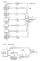
- Fig. 4 is a circuit diagram showing an example of a conventional variable equalizer which forms a part of the background to the present invention.
- An input signal input to an input terminal 1 branches through a branch circuit 2.
- One branch of the input signal is applied to an attenuation setting circuit 4 having a coefficient -an and the remaining signal is input to the next branch circuit 2 through a delay line 3 having a delay amount T.
- the respective branched signals from a succession of branch circuits 2 are applied to respective attenuation setting circuits having respective attenuation amounts.
- the signals from the attenuation setting circuits 4, 4, ..., are all applied to an adder 5 and the resultant signal is output from the adder 5 to an output terminal 6.
- variable equalizer ME by varying the amplitude frequency response and group delay frequency response while detecting the bit error rate (BER).
- BER bit error rate
- the bit error rate is more greatly affected by the group delay distortion than by the amplitude distortion and thus an operation for seeking such an optimum point is easily made if an optimum equalization amount for the group delay distortion can be set.
- a conventional variable equalizer has not been able to vary, for example, only the amplitude or only the group delay since the attenuation amounts of the attenuation setting circuits 4, 4, ..., are arbitrarily set. Accordingly, this means that it is difficult to seek an optimum point with a conventional variable equalizer in a TDMA communication system in which the influence of the group delay frequency response is greater than that of the amplitude frequency response.
- the attenuation amounts of a conventional variable equalizer determine the amplitude frequency response and group delay frequency response, respectively, the amount by which these frequency response characteristics vary when a single attenuation amount varies could not be known without a large amount of simulation data since such variation differs depending on other coefficients. For this reason, it cannot easily be confirmed how the amplitude and group delay are equalized.
- FIG. 5 Another variable equalizer as shown in Figure 5 has been already proposed by the present applicant, for example.
- an input signal applied from an input terminal 1 is distributed by a distributor 7.
- the signal distributor 7 divides a signal into three signals of the same level.
- a delay line 3 having a delay amount T is interposed in one path for one of the three signals
- a delay line 31 having a delay amount 2T is interposed in another path
- a polarity inverter 8 is interposed in the remaining path.
- the polarity inverter 8 is structured by a known transformer or transistor and the like and shifts the phase of an applied signal by 180°.
- the signal from the delay line 31 and the signal from the polarity inverter 8 are combined by an adder 9 and then applied to a variable attenuation setting circuit 10.
- the variable attenuation setting circuit 10 has a reverse polarity output.
- the output signal therefrom is combined with the output signal from the delay line 3 by an adder 11.
- the response characteristic G o ( ⁇ ) of the amplitude with respect to the frequency of the output signal B(w) and the response characteristic TB ( W ) of the delay amount with respect to the frequency of the output signal B(w) are provided the following equatinos (2) and (3), respectively.
- w is the angular frequency
- w 2nf wherein f is the frequency.
- Variation with frequency of the amplitude frequency response characteristic G o ( ⁇ ) and the group delay frequency response characteristic ⁇ B ( ⁇ ) where the coefficient I is larger than 0 (I>0) are shown in the Fig. 6.
- Fig. 6(A) shows the amplitude frequency response
- Fig. 6(B) shows the group delay frequency response, wherein the amplitude and delay amount varies in the direction of the arrow when the coefficient I is increased.
- the delay amount varies if the coefficient I is varied in the attenuation setting circuit 10.
- the amplitude as well as the delay amount varies with variation of the coefficient I and thus it is extremely difficult to utilize the Fig. 5, example as a variable equalizer in the TDMA communication system.
- a principal object of the present invention is to provide a variable group delay equalizer in which the variation in the amplitude when the delay amount is changed is very small, so that the equalizer can be effectively utilized in a TDMA communication system.
- the signals of each pair are combined, in one case with identical phase and in the other case with the signal of lead T inverted.
- Each combined signal is individually weighted and then combined with each other and the main signal and finally given a common weighting.
- the combined signal from the combination in the same phase is combined with an inverted signal divided from the main signal before it is individually weighted, but after having been halved in amplitude.
- the output signal from the filter is described by the following equation:
- the weights W i , W 2 and W 3 are to be individually and independently variable, since it appears (from the approximate transfer function given in the Abstract; W( ⁇ ) ⁇ W 1 [1+W 2 ⁇ +W 3 ⁇ 2 ]) that one will be used essentially to vary the amplitude distortion while another will be used essentially to vary the group delay and the third has overall effect. It should also be noted that the weights are complex quantities, including in-phase and quadrature components.
- a variable group delay equalizer in which a signal input is distributed into at least a main signal and first to fourth signals which are eventually recombined in an output signal, the said signals being subject to a pattern of delays whereby, relative to the absolute delay applied to the main signal, the first and second signals have respectively a time lead and a time lag of a first predetermined time period and the third and fourth signals have respectively a time lead and a time lag of a second predetermined time period, when recombined in the output signal, the equaliser having:
- the correction signal can reduce the amplitude distortion which would otherwise be present, and thus a variable group delay equalizer which is capable of varying a group delay frequency response without varying an amplitude frequency response can be obtained. If a plurality of variable signal attenuation means are adapted to be ganged with each other, it is easy to adjust such delay amounts. As seen in an embodiment, if simiJar variable signal attenuation means are ganged with each other, a variable group delay equalizer with a very simple circuit structure, but with a very high accuracy can be obtained at low cost.
- a preferred embodiment of the present invention is directed to an equalizer circuit for use in a transmitting apparatus and/or a receiving apparatus to an amplitude distortion and group delay distortion caused in a transmit/receive system, and which further comprises
- amplitude distortion and group delay distortion can be equalized independently and continuously and thus the group delay distortions which principally affect the bit error rate in a TDMA communication system, for example, can easily be equalized.
- the amplitude frequency response and group delay frequency response can be independently adjusted, it can easily be confirmed in what conditions the amplitude distortion and group delay distortion are equalized and thus reproducible data can easily be obtained without a large number of simulations.
- the present invention provides an equalizer comprising:
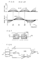
- Fig. 7 is a block diagram showing an equalizer circuit embodying the present invention for use in a TDMA communication system.
- a signal from an input terminal 101 is applied to an output terminal 102 through a variable amplitude equalizer VAE and a variable group delay equalizer VDE which are included in an equalizer circuit EQL. If and when the equalizer EQL is used, for example, in a TDMA communication system as shown in Fig.
- the input terminal 101 is connected to a modulator and the output terminal 102 is connected to a transmitter when the equalizer EQL is to be included in a transmitting system, and the input terminal 101 is connected to a receiver and the output terminal 102 is connected to a demodulator when the equalizer EQL is included in a receiving system.
- the variable amplitude equalizer VAE can vary the amplitude frequency response only, without varying the group delay frequency response
- the variable group delay equalizer VDE can vary the group delay frequency response only, without varying the amplitude frequency response.
- a fixed equalizer may also be used as necessary.
- Fig. 8 is a circuit diagram showing one example of a variable amplitude equalizer.
- the Fig. 8 embodiment is largely the same as the Fig. 5 arrangement except that a polarity inverter is omitted as compared with the variable equalizer as shown in Fig. 5. More particularly, an input signal from an input terminal 101 is distributed by a distributor 7. A signal which passes through a delay line 31 is combined with a signal which does not pass through the delay line by an adder 9 and the thus combined signal is applied to an adder 11 through a variable attenuation setting circuit 10 having an attenuation amount or coefficient k. In such a way, the adder 11 combines a main signal passing through the delay line 3 and a subsignal passing through a variable attenuation setting circuit 10 and outputs the combined signal to an output terminal 101'.
- the group delay frequency response characteristic TA ( W ) is flat.
- the variation of the amplitude frequency response characteristic G A (w) with the coefficient k is shown in Fig. 9. If the coefficient k is made larger, the amplitude varies in the direction of the arrow. More particularly, in the Fig. 8 embodiment, a variable amplitude equalizer VAE can be obtained which is capable of varying the amplitude frequency response without varying the group delay frequency response, by varying the coefficient k of the variable attenuation setting circuit 10.
- a variable attenuation setting circuit 10 includes a double balanced mixer DBM and a voltage generator VG for applying a control voltage thereto.
- the double balanced mixer DBM includes an input terminal LO, an output terminal RF and a control terminal IF.
- the double balanced mixer DBM comprises a transformer connected to the input terminal LO and a transformer connected to the output terminal RF, and four diodes D1 to D4 connected in a bridge manner between the two transformers.
- the control voltage generator VG comprises a variable resistor VR and a transistor Q1 to the base of which is applied a voltage from the variable resistor VR.
- the collector of the transistor Q1 and one end of the variable resistor VR are connected to a power supply +V and the emitter of the transistor Q1 and the other end of the variable resistor VR are connected to a power supply -V.
- the value of the resistance of the variable resistance VR is changed so that the control current Ic flows from the emitter of the transistor Q1 towards the control terminal IF.
- An output signal from the adder 9, for example, is applied to the input terminal LO of the double balanced mixer DBM and the output terminal RF is connected to an input of the adder 11.
- An emitter voltage Ve of the transistor Q1 is set within the range from +Ve to -Ve by adjusting the variable resistor VR.
- the voltage Ve causes a control current Ic to flow into the double balanced mixer DBM through the terminal IF, the direction of the current Ic depending on the polarity of the voltage Ve. If and when the polarity of the voltage Ve is plus, the diodes D1 and D3 become conductive and the diodes D2 and D4 are cutoff.
- variable attenuation setting circuit as shown in Fig. 10 can invert the polarity of a signal passing therethrough as well as vary the amplitude thereof.
- Fig. 12 is a circuit diagram showing an example of a variable group delay equalizer embodying the present invention.
- the variable group delay equalizer VDE comprises an input terminal 102' and an output terminal 102, the input terminal 102' being connected to, for example, an output terminal 101' as shown in Fig. 8.
- the output terminal 102 is connected to, for example, the transmitter TR or the demodulator DEM (Fig. 1).
- Theinput terminal 102' is connected to a distributor 7 and thus an input signal is distributed by the distributor 7 into the necessary number of signals (in this embodiment, the number is 5). Two of these five signals are applied to a delay circuit 12 and another two signals are applied to a correcting circuit 13. The remaining signal is applied to an adder 21 through a delay line 301 having a delay amount 2T.
- the two signals applied to the delay circuit 12 are delayed, respectively, by the delay lines 302 and 303 having delay amounts 3T and T, respectively, so that a signal of time lead of T and a signal of time delay of Tare obtained with respect to the reference which is the absolute delay amount (2T, in this example) of a main signal circuit, that is, the delay line 301, the output signal from the delay line 302 is a signal of time delay T with respect to the main signal and the output signal from the delay line 303 is a signal of time lead T with respect to the main signal.
- the output signal from the delay line 303 is applied to an adder 15 through a known polarity inverter 14, together with the output signal from the delay line 302.
- signals of a predetermined time lead T and time delay T with respect to the reference of the absolute delay amount of the main signal are combined at the same level but different polarity and the synthesized signal is applied to an adder 19.
- one of two signals from the distributor 7 to the correcting circuit 13 is directly applied to an adder 16 and the other is applied to the adder 16 through a delay line 304 having a delay amount 4T. Accordingly, in the correcting circuit 13, signals of a predetermined time lead 2T and time delay 2T with respect to the reference of the absolute delay amount of the main signal, are combined at the same level by the adder 16.
- variable attenuation setting circuit 18 An output signal from the adder 16 is applied to a variable attenuation setting circuit 18 through a known fixed attenuator 17.
- the variable attenuating setting circuit 18 has an attenuation amount or coefficient I, an output signal from the circuit 18 being applied to the adder 19.
- the adder 19 combines the output signal from the delay circuit 12 and the output signal from the correcting circuit 13 and applies the combined output to the adder 21 of the final stage through a variable attenuation setting circuit 20.
- the variable attenuation setting circuit 20 is ganged with the above described variable attenuation setting circuit 18. More specifically, these variable attenuation setting circuits 18 and 20 each comprise a double balanced mixer as shown in Fig. 10 and are controlled by the same voltage Ve from the voltage generator VG (Fig. 10). Therefore, in this embodiment, it is possible to vary the coefficients I of two attenuation setting circuits 18 and 20 in a ganged manner simply by varying the resistance of the variable resistor VR (Fig. 10
- the main signal circuit and the amplitude correcting circuit 13 are the same as in the variable amplitude equalizer VAE as shown in Fig. 8 and, assuming that the delay circuit 12 is not provided, only the amplitude frequency response varies, without variation of the group delay frequency response, when the coefficient I of the variable attenuation setting circuit 18 is varied.
- the period of repetition of amplitude variation in the correcting circuit 13 is 1/2T.
- the main signal circuit and the delay circuit have a period of repetition of amplitude variation of 1/2T.
- the period of the repetition of amplitude frequency response of the correcting circuit 13 and that in the delay circuit 12 are the same so that the amplitude variation in the delay circuit 12 can be cancelled by the output signal from the correcting circuit 13, which results in an extremely small amplitude variation.
- variable attenuation setting circuits 18 and 20 are ganged with each other and have the same coefficient I. Let it be assumed that the fixed attenuator 17 has an attenuator amount 6 dB, that is, the coefficient 0.5, the whole coefficient k is given in the following equation (8).
- Fig. 13(A) indicates the amplitude frequency response characteristic
- Fig. 13(B) indicates the group delay frequency response characteristic.
- the coefficient I of both variable attenuation setting circuits 18 and 20 are made larger, the amplitude and the delay amount vary, respectively, in the direction of the arrow.
- the group delay frequency response can be varied by varying the coefficient I while the variation of amplitude with frequency remains very small irrespective of variation of the coefficient I..
- the graph of Fig. 13 shows the amplitude variation and a delay amount variation when the coefficient 1>0. If the coefficient 1 ⁇ 0, the sign of the above described equation (10) is reversed and thus the lead and the lag of the delay amount with respect to the reference are reversed. However, the above described equation (9) is not reversed if the absolute value of the coefficient I is maintained even if the coefficient 1 ⁇ 0. More particularly, if and when the coefficient changes from plus to minus, the delay amount reverses and changes as shown in Fig. 14, but the amplitude simply repeats the variation shown in Fig. 13(A). Thus it will be understood that the Fig. 12 embodiment can vary the group delay frequency response only, without any amplitude variation.
- variable group delay equalizer VDE is employed as a variable equalizer in a TDMA communication system
- deterioration of a bit error rate due to group delay distortions only can be equalized independently.
- an operation for seeking an optimum point is readily performed as compared with a conventional case where an amplitude frequency response and a group delay frequency response change together.
- the respective amounts of equalization for the amplitude distortion and the delay distortion can be ascertained with certainty and thus reproducible data can be obtained, without a number of simulations, by using such a variable group delay equalizer and variable amplitude equalizer.
- Fig. 15 is a circuit diagram showing another embodiment of the present invention.
- the position of the variable attenuation setting circuit 20 is changed and correspondingly, the coefficient of the variable attenuation setting circuit 18' is changed.
- the variable attenuation setting circuit 20 is connected as a subsequent stage to the adder 19, but the variable attenuation setting circuit 20 can be interposed between the adders 15 and 19, as shown in Fig. 15, if the coefficient of the variable attenuation setting circuit 18' is squared to become I 2 .
- variable attenuation setting circuits may be ganged with each other so that the amplitude of the output signal from the correcting circuit 13 is multiplied by the square of the multiplication factor applied to the amplitude of the output signal from the delay circuit 12, that is, it is attenuated by twice as much on a decibel scale.
- Fig. 16 is a circuit diagram showing another embodiment of the present invention.
- the Fig. 16 embodiment is the same as the Fig. 12 embodiment except that a combination of conventional branch circuits and delay lines as shown in Fig. 4 is used as a signal withdrawing means.
- Fig. 17 is a circuit diagram showing a further embodiment of the present invention.
- the Fig. 17 embodiment is structured such that the delay circuit and the correcting circuit comprise a plurality of sets of signal paths, respectively.
- the delay circuit 12' has adders 15 and 15'which are combined by adder 24, and in a corresponding manner the correcting circuit 13' has adders 16 and 16' which are combined by adder 25.
- the output signal of the adder 15' is attenuated by a fixed attenuator 22 and the output signal from the adder 16' is attenuated by a fixed attenuator 22'.
- the fixed attenuators 22 and 22' have coefficients m and m 2 , respectively.
- the amplitude variation of a signal passing through the adder 15' is cancelled by an amplitude variation of a signal passing through the adder 16', by setting the coefficients of fixed attenuators 22 and 22' at m and m 2 , and consequently, the delay amount only of the signal obtained at the output terminal 102 can be changed by varying the coefficients I of the variable attenuation setting circuits 18 and 20 in a ganged manner.
- variable attenuation-setting circuit In the above described embodiments, a double balanced mixer is used as one example of a variable attenuation-setting circuit. However, it will be readily understood by those skilled in the art that such a variable attenuation setting circuit can be achieved by other circuit structures.
- a 180° phase shifter is used as the polarity inverters 14,14'.
- a 180° combiner or a 90° distributor may be used as such a polarity inverter.
- the two signals applied to the adder 15 must ultimately have inverse polarities from each other.
- variable attenuation setting circuits 18 (or 18') and 20 may be used with the variable attenuation setting circuits 18 (or 18') and 20, which would not themselves reverse the polarity.
- the circuits 18 (18') and 20 must be ganged with each other so that the respective amplitudes of the output signal from the delay circuit 12 and the output signal from the correcting circuit 13 are attenuated in effect in a constant log ratio, but the position in which they are inserted and the coefficients may be arbitrarily selected as long as this requirement is satisfied.
- variable attenuation setting circuits having a predetermined coefficient or attenuation amount may be ganged with each other and disposed in the respective signal paths provided in the delay circuit 12 and the correcting circuit 13.
- variable group delay equalizer can, of course, be used in an FDM communication system and the like.
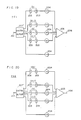
- Fig. 18 is a circuit diagram showing a preferred example of a group delay equalizer which can be used in one embodiment of the present invention.
- an input signal input to an input terminal 201 is applied to a distributor 207.
- the distributor 207 is comprised of a combination of hybrid circuits 208, 208, ..., which divide a signal into two signals at the same signal level.
- the input signal is applied to the necessary number of signal lines by the distributor 207.
- 0 to 2n delay lines, each having a delay amount T, respectively are interposed in the respective signals lines.
- attenuation setting circuits 204, 204, ..., having coefficients a o , +a, and -a,, ..., +an and -an are interposed.
- the distributor 207 since the distributor 207 has the structure of a stack of hybrid circuits 208, the signals applied to the attenuation setting circuit 204 having a coefficient +a, and the attenuation setting circuit 204 having a coefficient -a i can have the same signal level as each other. Similarly, the signals applied to the attenuation setting circuit 204 having a coefficient +an and the attenuation setting circuit 204 having the coefficient -an can have the same signal level as each other.
- a circuit having the same characteristic as a known group delay equalizer can be obtained by properly setting coefficients a o to an in the attenuation setting circuits 204, 204, ....
- the delay characteristic T ( W ) can be changed by varying the coefficient I.
- the equivalent conventional equalizer as shown in Fig. 4 required a correcting means since the signal levels of the different signals input to the attenuation setting circuit are different.
- the structure of the circuit of such an equalizer is large and expensive as well as complicated.
- such correcting means can be omitted because the distribution ratio in the distributor 207 can be set adequately.
- the distributor 207 provides signals having the same signal level to both members of any pair of lines having attenuators +a and -a, and total delays +T and -T, relative to the absolute delay on the a o line.
- the influence of the amplitude frequency characteristic can be greatly reduced. More particularly, in a conventional apparatus in Fig.
- a main signal that is, a signal passing through the attenuation setting circuit having a coefficient a o , comes to have an amplitude frequency characteristic depending on the frequency characteristics of the branch circuits through which the signal passes thereto.
- the level of the main signal is the largest as compared with the other signals and consequently, such an amplitude frequency characteristic of the branch circuits has a large effect on the frequency response characteristic of an output signal output from -the output terminal 6.
- Fig. 19 is a circuit diagram showing another example of a group delay equalizer embodying the present invention.
- a signal distributor 207' divides an applied input signal into signals of the same level.
- a combination of hybrid circuits as shown in Fig. 18 can be used as the distributor 207', other structures may be used.
- all of the distributed output levels of the distributor 207' can be made to be the same and thus correcting means which was required in the prior art is not required.
- Fig. 20 is a circuit diagram showing an amplitude equalizer as another embodiment of the present invention. Since, as described in the foregoing, an amplitude equalizer is different from a group delay equalizer only in the polarity of some of the signals, the detailed description may be omitted here. Even in the Fig. 20 embodiment, the level correcting means can be eliminated, just as in the Fig. 19 embodiment.
- variable group delay equalizer or a variable amplitude equalizer can be obtained, respectively, by making each attenuation setting circuit variable.
- a known double balanced mixer is available as such a variable attenuation setting circuit.
- means for correcting a difference in levels due to an insertion loss, which was conventionally required, can be omitted, since the signal level to each branch signal line can be arbitrarily set by a signal distributor means.
Landscapes
- Engineering & Computer Science (AREA)
- Power Engineering (AREA)
- Computer Networks & Wireless Communication (AREA)
- Signal Processing (AREA)
- Cable Transmission Systems, Equalization Of Radio And Reduction Of Echo (AREA)
- Filters And Equalizers (AREA)
Claims (17)
Applications Claiming Priority (6)
| Application Number | Priority Date | Filing Date | Title |
|---|---|---|---|
| JP178552/81 | 1981-11-05 | ||
| JP178567/81 | 1981-11-05 | ||
| JP17855181A JPS5879321A (ja) | 1981-11-05 | 1981-11-05 | 等化器 |
| JP178551/81 | 1981-11-05 | ||
| JP17855281A JPS5879322A (ja) | 1981-11-05 | 1981-11-05 | 可変遅延等化器 |
| JP17856781A JPS5879323A (ja) | 1981-11-05 | 1981-11-05 | 通信装置の等化回路 |
Publications (2)
| Publication Number | Publication Date |
|---|---|
| EP0079204A1 EP0079204A1 (de) | 1983-05-18 |
| EP0079204B1 true EP0079204B1 (de) | 1987-01-28 |
Family
ID=27324601
Family Applications (1)
| Application Number | Title | Priority Date | Filing Date |
|---|---|---|---|
| EP82305871A Expired EP0079204B1 (de) | 1981-11-05 | 1982-11-04 | Entzerrerkreis für Nachrichteneinheit |
Country Status (3)
| Country | Link |
|---|---|
| US (1) | US4491808A (de) |
| EP (1) | EP0079204B1 (de) |
| DE (1) | DE3275341D1 (de) |
Families Citing this family (13)
| Publication number | Priority date | Publication date | Assignee | Title |
|---|---|---|---|---|
| AU568117B2 (en) * | 1983-02-25 | 1987-12-17 | Mitsubishi Denki Kabushiki Kaisha | Variable group delay equalizer |
| JPH0721843B2 (ja) * | 1983-12-26 | 1995-03-08 | 株式会社日立製作所 | 波形等化器 |
| CA1275710C (en) * | 1986-08-18 | 1990-10-30 | Toshiaki Suzuki | Amplitude equalizer |
| JP2840155B2 (ja) * | 1992-03-19 | 1998-12-24 | 富士通株式会社 | 等化方法 |
| US5291156A (en) * | 1993-02-10 | 1994-03-01 | At&T Bell Laboratories | Method and apparatus for imparting positive phase slope to a narrowband signal |
| DE19707675A1 (de) * | 1997-02-26 | 1998-08-27 | Bosch Gmbh Robert | Anordnung zur Entzerrung eines Frequenzsignals, insbesondere für eine Satellitenkommunikationsanlage |
| US6317013B1 (en) | 1999-08-16 | 2001-11-13 | K & L Microwave Incorporated | Delay line filter |
| US6664869B2 (en) | 2001-03-30 | 2003-12-16 | Delaware Capital Formation | Delay line filters using multiple in-line four-input couplers |
| US6600388B2 (en) | 2001-03-30 | 2003-07-29 | Delaware Capital Formation, Inc. | Electronic variable delay line filters using two in-line varactor-controlled four-input couplers allowing variable delay |
| US20030093809A1 (en) * | 2001-09-28 | 2003-05-15 | Zhengjin Shu | Channel equalization |
| US6801098B2 (en) * | 2002-01-31 | 2004-10-05 | Remec, Inc | Group delay equalizer integrated with a wideband distributed amplifier monolithic microwave integrated circuit |
| US7359680B2 (en) * | 2004-09-14 | 2008-04-15 | Telefonaktiebolaget Lm Ericsson (Publ) | Delay calibration in polar modulation transmitters |
| CN111179804B (zh) * | 2020-01-13 | 2023-04-18 | 合肥鑫晟光电科技有限公司 | 一种时序控制器、显示装置、信号调整方法 |
Family Cites Families (8)
| Publication number | Priority date | Publication date | Assignee | Title |
|---|---|---|---|---|
| DE1085922B (de) * | 1958-09-12 | 1960-07-28 | Siemens Ag | Echoentzerrer fuer Breitband-uebertragungssysteme |
| BE637477A (de) * | 1962-09-17 | |||
| SE375671B (de) * | 1967-03-16 | 1975-04-21 | Fujitsu Ltd | |
| US3609599A (en) * | 1970-03-18 | 1971-09-28 | Bell Telephone Labor Inc | Time delay equalizer utilizing a plurality of cascaded directional filters |
| US3737808A (en) * | 1971-12-29 | 1973-06-05 | Honeywell Inf Systems | Pulse shaping network |
| DE2512752C3 (de) * | 1975-03-22 | 1982-01-28 | Licentia Patent-Verwaltungs-Gmbh, 6000 Frankfurt | Schaltungsanordnung zur Entzerrung von Laufzeiten in Empfängern von Richtfunkanlagen |
| US4071782A (en) * | 1976-06-28 | 1978-01-31 | International Video Corporation | Phaseless equalizer |
| US4064422A (en) * | 1976-08-31 | 1977-12-20 | The United States Of America As Represented By The Secretary Of The Air Force | Weight multiplier for use in an adapter processor |
-
1982
- 1982-09-14 US US06/418,164 patent/US4491808A/en not_active Expired - Lifetime
- 1982-11-04 DE DE8282305871T patent/DE3275341D1/de not_active Expired
- 1982-11-04 EP EP82305871A patent/EP0079204B1/de not_active Expired
Also Published As
| Publication number | Publication date |
|---|---|
| US4491808A (en) | 1985-01-01 |
| DE3275341D1 (en) | 1987-03-05 |
| EP0079204A1 (de) | 1983-05-18 |
Similar Documents
| Publication | Publication Date | Title |
|---|---|---|
| US3781722A (en) | Digitally variable delay time system | |
| US8792545B2 (en) | Balancing amplitude and phase | |
| US5862455A (en) | Fading simulator | |
| US4491808A (en) | Equalizer circuit for use in communication unit | |
| GB1105958A (en) | Correction of distortion in transversal equilizers | |
| JPS60236529A (ja) | 複数伝搬路による干渉の擬似試験方法および装置 | |
| US4373207A (en) | Space diversity signal combiner | |
| US4258340A (en) | Amplitude equalizer | |
| US4333063A (en) | Amplitude equalizer | |
| RU2001128744A (ru) | Система и способ для оценки мощности | |
| US4298983A (en) | Automatic equalization system in FM communication circuit | |
| US4607377A (en) | Transversal type equalizer apparatus | |
| US4730342A (en) | Equalizer circuit for use in communication unit | |
| US3553606A (en) | System for providing adjusting signals to a transversal filter equalizer | |
| EP0257526B1 (de) | Amplitudentzerrer | |
| US4013960A (en) | Quadraphase modulator | |
| US5506549A (en) | Cable equalizer | |
| US5025453A (en) | Method of measuring the signature of digital transmission equipment, and apparatus for implementing such a method | |
| US3268836A (en) | Transversal filter for correcting or synthesizing echoes accompanying unidirectionalprincipal pulse, including automatic means preventing unidirectional bias of output transformer core | |
| KR950012821B1 (ko) | 디지탈 비순환형 필터 형태의 등화기를 갖는 vhf카 라디오 | |
| US3660785A (en) | Transversal equalizer | |
| US4837780A (en) | Transmit line buildout circuits | |
| JPS6349929B2 (de) | ||
| JPS6232870B2 (de) | ||
| US4607241A (en) | Transversal filter equalizer with minimally interactive adjustments |
Legal Events
| Date | Code | Title | Description |
|---|---|---|---|
| PUAI | Public reference made under article 153(3) epc to a published international application that has entered the european phase |
Free format text: ORIGINAL CODE: 0009012 |
|
| AK | Designated contracting states |
Designated state(s): DE FR GB |
|
| 17P | Request for examination filed |
Effective date: 19831105 |
|
| GRAA | (expected) grant |
Free format text: ORIGINAL CODE: 0009210 |
|
| AK | Designated contracting states |
Kind code of ref document: B1 Designated state(s): DE FR GB |
|
| REF | Corresponds to: |
Ref document number: 3275341 Country of ref document: DE Date of ref document: 19870305 |
|
| ET | Fr: translation filed | ||
| PLBE | No opposition filed within time limit |
Free format text: ORIGINAL CODE: 0009261 |
|
| STAA | Information on the status of an ep patent application or granted ep patent |
Free format text: STATUS: NO OPPOSITION FILED WITHIN TIME LIMIT |
|
| 26N | No opposition filed | ||
| REG | Reference to a national code |
Ref country code: GB Ref legal event code: 746 Effective date: 19951026 |
|
| REG | Reference to a national code |
Ref country code: FR Ref legal event code: D6 |
|
| PGFP | Annual fee paid to national office [announced via postgrant information from national office to epo] |
Ref country code: DE Payment date: 20001025 Year of fee payment: 19 |
|
| PGFP | Annual fee paid to national office [announced via postgrant information from national office to epo] |
Ref country code: GB Payment date: 20001101 Year of fee payment: 19 |
|
| PGFP | Annual fee paid to national office [announced via postgrant information from national office to epo] |
Ref country code: FR Payment date: 20001110 Year of fee payment: 19 |
|
| PG25 | Lapsed in a contracting state [announced via postgrant information from national office to epo] |
Ref country code: GB Free format text: LAPSE BECAUSE OF NON-PAYMENT OF DUE FEES Effective date: 20011104 |
|
| REG | Reference to a national code |
Ref country code: GB Ref legal event code: IF02 |
|
| GBPC | Gb: european patent ceased through non-payment of renewal fee |
Effective date: 20011104 |
|
| PG25 | Lapsed in a contracting state [announced via postgrant information from national office to epo] |
Ref country code: DE Free format text: LAPSE BECAUSE OF NON-PAYMENT OF DUE FEES Effective date: 20020702 |
|
| PG25 | Lapsed in a contracting state [announced via postgrant information from national office to epo] |
Ref country code: FR Free format text: LAPSE BECAUSE OF NON-PAYMENT OF DUE FEES Effective date: 20020730 |
|
| REG | Reference to a national code |
Ref country code: FR Ref legal event code: ST |
|
| REG | Reference to a national code |
Ref country code: FR Ref legal event code: ST |