EP0081956A1 - Lasers à injection avec guides d'ondes intégrés - Google Patents
Lasers à injection avec guides d'ondes intégrés Download PDFInfo
- Publication number
- EP0081956A1 EP0081956A1 EP82306438A EP82306438A EP0081956A1 EP 0081956 A1 EP0081956 A1 EP 0081956A1 EP 82306438 A EP82306438 A EP 82306438A EP 82306438 A EP82306438 A EP 82306438A EP 0081956 A1 EP0081956 A1 EP 0081956A1
- Authority
- EP
- European Patent Office
- Prior art keywords
- laser
- active region
- active layer
- regions
- active
- Prior art date
- Legal status (The legal status is an assumption and is not a legal conclusion. Google has not performed a legal analysis and makes no representation as to the accuracy of the status listed.)
- Granted
Links
- 238000002347 injection Methods 0.000 title claims abstract description 22
- 239000007924 injection Substances 0.000 title claims abstract description 22
- 230000006798 recombination Effects 0.000 claims abstract description 10
- 238000005215 recombination Methods 0.000 claims abstract description 10
- 238000013139 quantization Methods 0.000 claims abstract description 3
- 230000005855 radiation Effects 0.000 claims description 20
- 230000001902 propagating effect Effects 0.000 claims description 9
- 238000005253 cladding Methods 0.000 claims description 7
- 239000000758 substrate Substances 0.000 claims description 4
- 239000004065 semiconductor Substances 0.000 claims description 3
- 230000005476 size effect Effects 0.000 abstract description 4
- 239000010410 layer Substances 0.000 description 68
- 229910001218 Gallium arsenide Inorganic materials 0.000 description 19
- 230000008878 coupling Effects 0.000 description 6
- 238000010168 coupling process Methods 0.000 description 6
- 238000005859 coupling reaction Methods 0.000 description 6
- 238000000034 method Methods 0.000 description 6
- 239000000969 carrier Substances 0.000 description 5
- 230000003287 optical effect Effects 0.000 description 5
- 239000000463 material Substances 0.000 description 4
- 230000008859 change Effects 0.000 description 3
- 239000000203 mixture Substances 0.000 description 3
- 238000001451 molecular beam epitaxy Methods 0.000 description 3
- 230000007704 transition Effects 0.000 description 3
- 238000010521 absorption reaction Methods 0.000 description 2
- 229910045601 alloy Inorganic materials 0.000 description 2
- 239000000956 alloy Substances 0.000 description 2
- 229910052782 aluminium Inorganic materials 0.000 description 2
- XAGFODPZIPBFFR-UHFFFAOYSA-N aluminium Chemical compound [Al] XAGFODPZIPBFFR-UHFFFAOYSA-N 0.000 description 2
- 230000004888 barrier function Effects 0.000 description 2
- 230000015556 catabolic process Effects 0.000 description 2
- 238000005229 chemical vapour deposition Methods 0.000 description 2
- 238000006731 degradation reaction Methods 0.000 description 2
- 238000000151 deposition Methods 0.000 description 2
- 230000008021 deposition Effects 0.000 description 2
- 230000000694 effects Effects 0.000 description 2
- 230000006870 function Effects 0.000 description 2
- 230000007246 mechanism Effects 0.000 description 2
- 229910052751 metal Inorganic materials 0.000 description 2
- 239000002184 metal Substances 0.000 description 2
- 230000008569 process Effects 0.000 description 2
- 230000009471 action Effects 0.000 description 1
- 238000003491 array Methods 0.000 description 1
- QVGXLLKOCUKJST-UHFFFAOYSA-N atomic oxygen Chemical compound [O] QVGXLLKOCUKJST-UHFFFAOYSA-N 0.000 description 1
- 230000008901 benefit Effects 0.000 description 1
- 238000011109 contamination Methods 0.000 description 1
- 239000013078 crystal Substances 0.000 description 1
- 230000007547 defect Effects 0.000 description 1
- 238000005530 etching Methods 0.000 description 1
- 230000005284 excitation Effects 0.000 description 1
- 229910052733 gallium Inorganic materials 0.000 description 1
- 230000010354 integration Effects 0.000 description 1
- 230000000873 masking effect Effects 0.000 description 1
- 229910052760 oxygen Inorganic materials 0.000 description 1
- 239000001301 oxygen Substances 0.000 description 1
- 230000000737 periodic effect Effects 0.000 description 1
- 238000005036 potential barrier Methods 0.000 description 1
- 239000002356 single layer Substances 0.000 description 1
- 230000007480 spreading Effects 0.000 description 1
Images


Classifications
-
- H—ELECTRICITY
- H01—ELECTRIC ELEMENTS
- H01S—DEVICES USING THE PROCESS OF LIGHT AMPLIFICATION BY STIMULATED EMISSION OF RADIATION [LASER] TO AMPLIFY OR GENERATE LIGHT; DEVICES USING STIMULATED EMISSION OF ELECTROMAGNETIC RADIATION IN WAVE RANGES OTHER THAN OPTICAL
- H01S5/00—Semiconductor lasers
- H01S5/10—Construction or shape of the optical resonator, e.g. extended or external cavity, coupled cavities, bent-guide, varying width, thickness or composition of the active region
- H01S5/16—Window-type lasers, i.e. with a region of non-absorbing material between the active region and the reflecting surface
-
- H—ELECTRICITY
- H01—ELECTRIC ELEMENTS
- H01S—DEVICES USING THE PROCESS OF LIGHT AMPLIFICATION BY STIMULATED EMISSION OF RADIATION [LASER] TO AMPLIFY OR GENERATE LIGHT; DEVICES USING STIMULATED EMISSION OF ELECTROMAGNETIC RADIATION IN WAVE RANGES OTHER THAN OPTICAL
- H01S5/00—Semiconductor lasers
- H01S5/10—Construction or shape of the optical resonator, e.g. extended or external cavity, coupled cavities, bent-guide, varying width, thickness or composition of the active region
-
- H—ELECTRICITY
- H01—ELECTRIC ELEMENTS
- H01S—DEVICES USING THE PROCESS OF LIGHT AMPLIFICATION BY STIMULATED EMISSION OF RADIATION [LASER] TO AMPLIFY OR GENERATE LIGHT; DEVICES USING STIMULATED EMISSION OF ELECTROMAGNETIC RADIATION IN WAVE RANGES OTHER THAN OPTICAL
- H01S5/00—Semiconductor lasers
- H01S5/02—Structural details or components not essential to laser action
- H01S5/026—Monolithically integrated components, e.g. waveguides, monitoring photo-detectors, drivers
-
- H—ELECTRICITY
- H01—ELECTRIC ELEMENTS
- H01S—DEVICES USING THE PROCESS OF LIGHT AMPLIFICATION BY STIMULATED EMISSION OF RADIATION [LASER] TO AMPLIFY OR GENERATE LIGHT; DEVICES USING STIMULATED EMISSION OF ELECTROMAGNETIC RADIATION IN WAVE RANGES OTHER THAN OPTICAL
- H01S5/00—Semiconductor lasers
- H01S5/10—Construction or shape of the optical resonator, e.g. extended or external cavity, coupled cavities, bent-guide, varying width, thickness or composition of the active region
- H01S5/1053—Comprising an active region having a varying composition or cross-section in a specific direction
- H01S5/106—Comprising an active region having a varying composition or cross-section in a specific direction varying thickness along the optical axis
-
- H—ELECTRICITY
- H01—ELECTRIC ELEMENTS
- H01S—DEVICES USING THE PROCESS OF LIGHT AMPLIFICATION BY STIMULATED EMISSION OF RADIATION [LASER] TO AMPLIFY OR GENERATE LIGHT; DEVICES USING STIMULATED EMISSION OF ELECTROMAGNETIC RADIATION IN WAVE RANGES OTHER THAN OPTICAL
- H01S5/00—Semiconductor lasers
- H01S5/10—Construction or shape of the optical resonator, e.g. extended or external cavity, coupled cavities, bent-guide, varying width, thickness or composition of the active region
- H01S5/16—Window-type lasers, i.e. with a region of non-absorbing material between the active region and the reflecting surface
- H01S5/164—Window-type lasers, i.e. with a region of non-absorbing material between the active region and the reflecting surface with window regions comprising semiconductor material with a wider bandgap than the active layer
-
- H—ELECTRICITY
- H01—ELECTRIC ELEMENTS
- H01S—DEVICES USING THE PROCESS OF LIGHT AMPLIFICATION BY STIMULATED EMISSION OF RADIATION [LASER] TO AMPLIFY OR GENERATE LIGHT; DEVICES USING STIMULATED EMISSION OF ELECTROMAGNETIC RADIATION IN WAVE RANGES OTHER THAN OPTICAL
- H01S5/00—Semiconductor lasers
- H01S5/20—Structure or shape of the semiconductor body to guide the optical wave ; Confining structures perpendicular to the optical axis, e.g. index or gain guiding, stripe geometry, broad area lasers, gain tailoring, transverse or lateral reflectors, special cladding structures, MQW barrier reflection layers
- H01S5/2004—Confining in the direction perpendicular to the layer structure
-
- H—ELECTRICITY
- H01—ELECTRIC ELEMENTS
- H01S—DEVICES USING THE PROCESS OF LIGHT AMPLIFICATION BY STIMULATED EMISSION OF RADIATION [LASER] TO AMPLIFY OR GENERATE LIGHT; DEVICES USING STIMULATED EMISSION OF ELECTROMAGNETIC RADIATION IN WAVE RANGES OTHER THAN OPTICAL
- H01S5/00—Semiconductor lasers
- H01S5/30—Structure or shape of the active region; Materials used for the active region
- H01S5/305—Structure or shape of the active region; Materials used for the active region characterised by the doping materials used in the laser structure
-
- H—ELECTRICITY
- H01—ELECTRIC ELEMENTS
- H01S—DEVICES USING THE PROCESS OF LIGHT AMPLIFICATION BY STIMULATED EMISSION OF RADIATION [LASER] TO AMPLIFY OR GENERATE LIGHT; DEVICES USING STIMULATED EMISSION OF ELECTROMAGNETIC RADIATION IN WAVE RANGES OTHER THAN OPTICAL
- H01S5/00—Semiconductor lasers
- H01S5/30—Structure or shape of the active region; Materials used for the active region
- H01S5/32—Structure or shape of the active region; Materials used for the active region comprising PN junctions, e.g. hetero- or double- heterostructures
- H01S5/3211—Structure or shape of the active region; Materials used for the active region comprising PN junctions, e.g. hetero- or double- heterostructures characterised by special cladding layers, e.g. details on band-discontinuities
-
- H—ELECTRICITY
- H01—ELECTRIC ELEMENTS
- H01S—DEVICES USING THE PROCESS OF LIGHT AMPLIFICATION BY STIMULATED EMISSION OF RADIATION [LASER] TO AMPLIFY OR GENERATE LIGHT; DEVICES USING STIMULATED EMISSION OF ELECTROMAGNETIC RADIATION IN WAVE RANGES OTHER THAN OPTICAL
- H01S5/00—Semiconductor lasers
- H01S5/30—Structure or shape of the active region; Materials used for the active region
- H01S5/32—Structure or shape of the active region; Materials used for the active region comprising PN junctions, e.g. hetero- or double- heterostructures
- H01S5/3211—Structure or shape of the active region; Materials used for the active region comprising PN junctions, e.g. hetero- or double- heterostructures characterised by special cladding layers, e.g. details on band-discontinuities
- H01S5/3216—Structure or shape of the active region; Materials used for the active region comprising PN junctions, e.g. hetero- or double- heterostructures characterised by special cladding layers, e.g. details on band-discontinuities quantum well or superlattice cladding layers
-
- H—ELECTRICITY
- H01—ELECTRIC ELEMENTS
- H01S—DEVICES USING THE PROCESS OF LIGHT AMPLIFICATION BY STIMULATED EMISSION OF RADIATION [LASER] TO AMPLIFY OR GENERATE LIGHT; DEVICES USING STIMULATED EMISSION OF ELECTROMAGNETIC RADIATION IN WAVE RANGES OTHER THAN OPTICAL
- H01S5/00—Semiconductor lasers
- H01S5/30—Structure or shape of the active region; Materials used for the active region
- H01S5/34—Structure or shape of the active region; Materials used for the active region comprising quantum well or superlattice structures, e.g. single quantum well [SQW] lasers, multiple quantum well [MQW] lasers or graded index separate confinement heterostructure [GRINSCH] lasers
- H01S5/3428—Structure or shape of the active region; Materials used for the active region comprising quantum well or superlattice structures, e.g. single quantum well [SQW] lasers, multiple quantum well [MQW] lasers or graded index separate confinement heterostructure [GRINSCH] lasers layer orientation perpendicular to the substrate
Definitions
- This invention relates to injection semiconductor lasers and in particular to such lasers with integral quantum size effect transparent waveguiding in the active layer.
- These lasers may be of the quantum well type.
- Quantum well heterostructure (QWH) lasers have attracted a large amount of interest in recent years because of the belief that quantum effects in the active regions of these lasers will provide improved operating characteristics in these lasers over the conventional double heterostructure injection lasers.
- a QWH laser basically comprises a heterostructure device with an active region comprising a single layer or multiple layers comprising a series of very thin heterostructure alternating layers of materials having different bandgapsand refractive indices.
- the quantum well active region comprises multiple alternate layers of Al x Ga l-x As and GaAs.
- the Al x Ga l-x As layers where x may be approximately 0.3 to 1.0) forms coupling barriers in the active region whereas the GaAs layers form wells.
- the size or thickness, L s , of the barriers may be about 1 to 5nm while the size or thickness, L z , of the wells may be about 3 to 5 nm where L B and L Z are generally equal to or less than 5 nm but may be greater or less compared to one another.
- quantum well lasers by confining the carriers (holes and electrons) to very thin active layers, the energy level of the lowest energy states will be modified and raised to one or more steps above the band edge, i.e., will shift the lowest confined carrier transitions E, more above the energy gap Eg.
- phonon, (LO) assistance is present in this state transition so that carriers have additional states to transfer to before recombining and producing radiation. These additional lower energy states are believed to be important in the radiation recombination emission from the QWH laser. Said in simpler terms, a phonon (LO) transition can assist in the recombination mechanism to make an indirect bandgap situation due to material difference function more like a direct bandgap phenomenon.
- Q WH mechanism provides phonon assisted radiative recombination to scatter carriers (electrons) to lower energies before recombining to provide photons and stimulated lasing action.
- Dupuis et al "Continuous 300 K Laser Operation of Single-Quantum-Well Al x Ga l-x As-GaAs Heterostructure Diodes Grown by Metalorganic Chemical Vapor Deposition", Vol. 34, No. 4 pp. 265-267 (February 15, 1979); N. Holonyak et al, “Phonon-Sideband MO-CVD Quantum-Well Al x Ga l-x As-GaAs Heterostructure Laser", Applied Physics Letters Vol. 34, No. 8, pp. 502-505 (April 15, 1979); N.
- the conventional taper coupler is shown in the above-mentioned Xerox Disclosure Journal.
- the active region of p-GaAs may be formed on the transparent waveguide layer of n-Ga .9 Al .1 As by masking techniques
- the n-type Ga .9 Al .1 As layer is a wider gap material than the p-type active region to serve as an efficient transparent waveguide and has some doping concentration in order to supply current to the active region, free carrier absorption in these transparent regions could be minimized if this waveguide layer were undoped or doped very lightly.
- the n-type transparent waveguide layer does not confine the injected carriers (holes) as desired because of the reduced potential barrier height As a result, the laser current threshold will vary more rapidly with temperature variations.
- the laser structures disclosed herein reduce or eliminate these disadvantages in the conventional tapered coupler heterostructure injection laser.
- the wider bandgap transparent waveguide layer may be eliminated from conventional tapered coupler heterostructure lasers and providing an active layer in the -regions where transparency is desired having an extremely small thickness (e.g., below 50 nm so that quantized electron states are produced in the conduction and hole states in the valence band.
- the active region of the active layer is thicker and is coupled into the thin active layer regions.
- the active region permits carrier recombination under lasing conditions for supporting propagation in an optical cavity that includes the very thin active layer regions that appear transparent to the propagating radiation.
- the transparency occurs because the active layer in these regions is so thin that the band structure is changed because of the quantum size effect.
- the electron states are quantized, radiation produced in the thicker active region will not be absorbed in the thinner active layer because of band structure change.
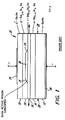
- Figure 1 discloses a conventional tapered coupler heterostructure injection laser 10 previously referenced and known in the art.
- Laser 10 comprises a plurality of consecutively deposited semiconductor layers, for example, of GaAs and GaAlAs of varying doping levels, thicknesses and composition.
- Substrate 12 may be n-GaAs.
- the tapered couplers 19 couple radiation produced in the active region 18 into the wider bandgap waveguide layer 16.
- the metal contact 24 on layer 22 only covers the region to be pumped, i.e., the active region 18.
- the bottom equalization 26 comprises the other electrode. No radiative recombination will occur due to current injection in the regions of the waveguide layer 16 beyond the active region 28 thereby reducing undesirable erosion- and degradation at the end facet 28.
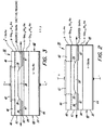
- the heterostructure injection laser 30 comprises the substrate 32 upon which is consecutively deposited by a selected fabricating process (e.g., MBE or MO-CVD) the cladding layer 34 ⁇ of n-Ga l-x Al y As, the active layer 36 with the active region 38 of undoped or very slightly doped (e.g., 3x10 17 ) quality, the cladding layer 41 of p-Ga l-x Al x As and the contact layer 40 of P +- GaAs.
- the appropriate metal contacts 42 and 44 are provided for forward biasing laser 30.
- Ion or proton implanted regions 46 may be provided for current confinement enhancement.
- carrier recombination occurs in active region 38 and radiation induced in this region is taper coupled at 39 into the thin active layer regions 47 of the active layer 36.
- an optical cavity is established between end facets 48 for the propagating radiation.
- the primary difference between injection laser 30 and injection laser 10 is that the active regions 47 are extremely thin, i.e., they are sufficiently thin to provide the quantization of electron states so that radiative recombination cannot occur.
- the thin regions 47 form a quantum well. They raise the effective band edge of the crystal so that an electron is not peimitted to transfer to the bottom of the well but can only stay in some higher energy state.
- the radiation produced in the active region will couple into the thin regions 47 because, even though this coupling may be somewhat weak, regions 47 are still the highest bandgap regions of the laser, next to region 38.
- the coupled radiation in regions 47 experiences transparency due to band structure change caused by the quantum size effect.
- the preferred thickness of the active region 38 may be approximately 50 to 10,00. nm while the thickness of the quantum well regions 47 may be approximately o. 5 to 5C nm preferably about 5 to 20 nm
- the molar fraction, x for example, may be approximately 0.3 . to 1.0.
- the active layer 36 may be two-dimensional i.e., regions 38 and 47 extend for the full width of the laser device, or three: - dimensional i.e., regions 38 and 47 comprise a strip completely confined on all sides by wider bandgap material.
- the epitaxial growth procedure for laser 30, as well as other lasers to be discussed, is as follows for the two-dimensional version .Epitaxial growth proceeds up to and including a very thin active layer. For example, in MO-CVD processing, and after deposition of layer 34, a very thin layer of about 5 nm of undoped GaAs is deposited on layer 34. Next, a mask having an elongated aperture is positioned on the thin active layer and the growth of layer 36 is continued.
- the mask is provided with an inner channel or chamber so that while the epitaxial deposition of region 38 proceeds, the tapered coupler regions 39 are formed due to the mask aperture geometry During the growth of layer 36, the aluminum-containing layer 34 is not contaminated because it is protected by previosuly deposited 5 nm thin GaAs layer.
- the epitaxial growth procedure may be followed.
- the thin initially grown active layer may have a thickness of about 40. nm Continued growth of the active layer is achieved as previously explained until an active region 38 of about 100 nm in thickness is produced.
- the active strip is formed by selective etching.
- Laser 50 in Figure 3 is identical to laser 30 in Figure 2 except for the additional transparent waveguide layer 52.
- Layer 52 is lightly doped (3x10 17 ) and may be comprised of n-Ga l- yAlyAs.
- Layer 52 functions also as a transparent waveguide to the propagating radiation.
- Layer 52 provides for taper coupling into a large transparent waveguide comprising the combination of regions 47 and layer 52 for enhanced waveguiding and low beam divergence.
- waveguiding layer 52 An alternative to the inclusion of waveguiding layer 52 would be to provide a transverse graded doping profile through cladding layer 34 so that the upper regions of this layer have a lighter doping profile as compared to its lower regions.
- the injection laser according to this invention may also have an active layer comprising of multiple quantum well passive regions.
- the laser 60 is identical to laser 30 in Figure 2 except for the quantum well structure in active layer 36 comprising alternating layers 36.1 of undoped GaAs/Ga l- yAlyAs. Layers 36.1 may, for example, be each about 4 to 5 nm thick. Regions 47 comprise multiquantum well unpumped regions while the. combination of active region 38 and the adjacent multiquantum well region 47.1 are pumped to provide carrier recombination under lasing conditions.
- the active region of laser 60 has been modified to comprise alternating layers 38.1 of undoped GaAs/GaAIAs, which together with region 47.1 form the active cavity region for laser 60.
- the quantum well layers 38 in the active region 38 preferably have a little larger thickness (e.g., 5 nm) compared to layers 36.1 (e.g., 4 nm ) to ensure that the waveguide regions 47 are more transparent to the propagating radiation.
- DFB or DBR laser structures may be incorporated.
- the thin active region/quantum well active layer may be incorporated in curved lasers or waveguides or in laser arrays formed on a single substrate. Additional wider bandgap layers may be added to both sides of the thin active region/quantum. well active layer to form a large optical cavity region.
- the large optical cavity region could be index graded so as to have a bandgap variation.
- the active region could be made very short.
- the periodic quantum well layers Figure 4 and 5 would be. designed with specific composition and layer thickness to optimize current threshold and longitudinal and fundamental transverse modes of operation.
- the current conducting stripe contact 42 could alternatively extend to the facets 48 of the laser rather than terminate over the active region as shown in the figures.
Landscapes
- Physics & Mathematics (AREA)
- Condensed Matter Physics & Semiconductors (AREA)
- General Physics & Mathematics (AREA)
- Electromagnetism (AREA)
- Optics & Photonics (AREA)
- Semiconductor Lasers (AREA)
Applications Claiming Priority (2)
| Application Number | Priority Date | Filing Date | Title |
|---|---|---|---|
| US32713681A | 1981-12-03 | 1981-12-03 | |
| US327136 | 1981-12-03 |
Publications (2)
| Publication Number | Publication Date |
|---|---|
| EP0081956A1 true EP0081956A1 (fr) | 1983-06-22 |
| EP0081956B1 EP0081956B1 (fr) | 1986-09-17 |
Family
ID=23275298
Family Applications (1)
| Application Number | Title | Priority Date | Filing Date |
|---|---|---|---|
| EP19820306438 Expired EP0081956B1 (fr) | 1981-12-03 | 1982-12-03 | Lasers à injection avec guides d'ondes intégrés |
Country Status (3)
| Country | Link |
|---|---|
| EP (1) | EP0081956B1 (fr) |
| JP (1) | JPS5898996A (fr) |
| DE (1) | DE3273383D1 (fr) |
Cited By (8)
| Publication number | Priority date | Publication date | Assignee | Title |
|---|---|---|---|---|
| GB2170044A (en) * | 1984-12-18 | 1986-07-23 | Canon Kk | Semiconductor laser |
| FR2596529A1 (fr) * | 1986-03-28 | 1987-10-02 | Thomson Csf | Guide d'onde optique en materiau semiconducteur, laser appliquant ce guide d'onde et procede de realisation |
| GB2188775A (en) * | 1986-02-13 | 1987-10-07 | Sharp Kk | A window semiconductor laser device and an epitaxial growth process for its production |
| DE4036000A1 (de) * | 1989-11-13 | 1991-05-16 | France Etat | Optischer verstaerker |
| NL9301195A (nl) * | 1992-07-09 | 1994-02-01 | Mitsubishi Electric Corp | Halfgeleiderlaser-inrichting. |
| EP0602579A1 (fr) * | 1992-12-15 | 1994-06-22 | Mitsubishi Denki Kabushiki Kaisha | Laser à semi-conducteur et méthode de fabrication |
| EP0641049A1 (fr) * | 1993-08-31 | 1995-03-01 | Fujitsu Limited | Dispositif optique à semi-conducteur et sa méthode de fabrication |
| US20240235163A9 (en) * | 2021-03-05 | 2024-07-11 | 3Sp Technologies | Semiconductor optoelectronic device |
Families Citing this family (3)
| Publication number | Priority date | Publication date | Assignee | Title |
|---|---|---|---|---|
| JP2836822B2 (ja) * | 1988-06-23 | 1998-12-14 | 日本電信電話株式会社 | 導波路型半導体光素子の製造方法 |
| CN103099171A (zh) * | 2012-12-06 | 2013-05-15 | 黄宵 | 一种卤肉配方 |
| CN103190591A (zh) * | 2012-12-13 | 2013-07-10 | 黄宵 | 一种浓香型香料 |
Citations (2)
| Publication number | Priority date | Publication date | Assignee | Title |
|---|---|---|---|---|
| US3978426A (en) * | 1975-03-11 | 1976-08-31 | Bell Telephone Laboratories, Incorporated | Heterostructure devices including tapered optical couplers |
| EP0031808A2 (fr) * | 1977-12-28 | 1981-07-08 | Western Electric Company, Incorporated | Procédé pour la croissance épitaxiale en phase liquide d'une deuxième couche d'un composé III-V sur une première couche d'un composé III-V comprenant de l'aluminium |
-
1982
- 1982-11-26 JP JP20749382A patent/JPS5898996A/ja active Granted
- 1982-12-03 DE DE8282306438T patent/DE3273383D1/de not_active Expired
- 1982-12-03 EP EP19820306438 patent/EP0081956B1/fr not_active Expired
Patent Citations (2)
| Publication number | Priority date | Publication date | Assignee | Title |
|---|---|---|---|---|
| US3978426A (en) * | 1975-03-11 | 1976-08-31 | Bell Telephone Laboratories, Incorporated | Heterostructure devices including tapered optical couplers |
| EP0031808A2 (fr) * | 1977-12-28 | 1981-07-08 | Western Electric Company, Incorporated | Procédé pour la croissance épitaxiale en phase liquide d'une deuxième couche d'un composé III-V sur une première couche d'un composé III-V comprenant de l'aluminium |
Non-Patent Citations (2)
| Title |
|---|
| PATENTS ABSTRACTS OF JAPAN, vol. 5, no. 103(E-64)[775], 3rd July 1981; & JP - A - 54 45 090 (NIPPON DENKI K.K.) (24-04-1981) * |
| XEROX DISCLOSURE JOURNAL, vol. 4, no. 5, September/October 1979, page 637, New York (USA); * |
Cited By (19)
| Publication number | Priority date | Publication date | Assignee | Title |
|---|---|---|---|---|
| GB2170044A (en) * | 1984-12-18 | 1986-07-23 | Canon Kk | Semiconductor laser |
| US4794611A (en) * | 1984-12-18 | 1988-12-27 | Canon Kabushiki Kaisha | Semiconductor laser having superlattice structure |
| GB2188775A (en) * | 1986-02-13 | 1987-10-07 | Sharp Kk | A window semiconductor laser device and an epitaxial growth process for its production |
| GB2188775B (en) * | 1986-02-13 | 1989-11-08 | Sharp Kk | A window semiconductor laser device and an epitaxial growth process for the production of the same |
| US5087587A (en) * | 1986-02-13 | 1992-02-11 | Sharp Kabushiki Kaisha | Epitaxial growth process for the production of a window semiconductor laser |
| FR2596529A1 (fr) * | 1986-03-28 | 1987-10-02 | Thomson Csf | Guide d'onde optique en materiau semiconducteur, laser appliquant ce guide d'onde et procede de realisation |
| EP0240400A1 (fr) * | 1986-03-28 | 1987-10-07 | Thomson-Csf | Guide d'onde optique en matériau semiconducteur, laser appliquant ce guide d'onde et procédé de réalisation |
| US4901321A (en) * | 1986-03-28 | 1990-02-13 | Thomson-Csf | Optical waveguide made solid state material laser applying this waveguide |
| FR2654523A1 (fr) * | 1989-11-13 | 1991-05-17 | France Etat | Amplificateur optique non resonnant a diode laser. |
| GB2238168A (en) * | 1989-11-13 | 1991-05-22 | Centre Nat Etd Telecomm | Laser diode optical amplifier |
| DE4036000A1 (de) * | 1989-11-13 | 1991-05-16 | France Etat | Optischer verstaerker |
| GB2238168B (en) * | 1989-11-13 | 1993-04-21 | Centre Nat Etd Telecomm | Laser diode optical amplifier |
| NL9301195A (nl) * | 1992-07-09 | 1994-02-01 | Mitsubishi Electric Corp | Halfgeleiderlaser-inrichting. |
| EP0602579A1 (fr) * | 1992-12-15 | 1994-06-22 | Mitsubishi Denki Kabushiki Kaisha | Laser à semi-conducteur et méthode de fabrication |
| US5486490A (en) * | 1992-12-15 | 1996-01-23 | Mitsubishi Denki Kabushiki Kaisha | Method of making semiconductor laser |
| EP0641049A1 (fr) * | 1993-08-31 | 1995-03-01 | Fujitsu Limited | Dispositif optique à semi-conducteur et sa méthode de fabrication |
| US5987046A (en) * | 1993-08-31 | 1999-11-16 | Fujitsu Limited | Optical semiconductor device and a method of manufacturing the same |
| US6238943B1 (en) | 1993-08-31 | 2001-05-29 | Fujitsu Limited | Optical semiconductor device and a method of manufacturing the same |
| US20240235163A9 (en) * | 2021-03-05 | 2024-07-11 | 3Sp Technologies | Semiconductor optoelectronic device |
Also Published As
| Publication number | Publication date |
|---|---|
| JPH0315356B2 (fr) | 1991-02-28 |
| DE3273383D1 (en) | 1986-10-23 |
| EP0081956B1 (fr) | 1986-09-17 |
| JPS5898996A (ja) | 1983-06-13 |
Similar Documents
| Publication | Publication Date | Title |
|---|---|---|
| US4546480A (en) | Injection lasers with quantum size effect transparent waveguiding | |
| US4731789A (en) | Clad superlattice semiconductor laser | |
| US4371966A (en) | Heterostructure lasers with combination active strip and passive waveguide strip | |
| US5208821A (en) | Buried heterostructure lasers using MOCVD growth over patterned substrates | |
| EP0661782A1 (fr) | Laser à semi-conducteur | |
| US4928285A (en) | Impurity-doped semiconductor laser device for single wavelength oscillation | |
| US8906721B2 (en) | Semiconductor light emitting device and method for manufacturing the same | |
| US4845725A (en) | Window laser with high power reduced divergence output | |
| JPH08107254A (ja) | マルチ波長レーザダイオードアレイ | |
| US4803691A (en) | Lateral superradiance suppressing diode laser bar | |
| US6470039B1 (en) | Semiconductor laser and production method thereof | |
| US5556804A (en) | Method of manufacturing semiconductor laser | |
| EP0081956B1 (fr) | Lasers à injection avec guides d'ondes intégrés | |
| JPH0656906B2 (ja) | 半導体レ−ザ装置 | |
| EP1081817B1 (fr) | Dispositif à semiconducteur | |
| JPH08222804A (ja) | 埋込ヘテロ構造半導体ダイオードレーザの製造方法 | |
| Zhukov et al. | Metamorphic lasers for 1.3-µm spectral range grown on GaAs substrates by MBE | |
| US5309465A (en) | Ridge waveguide semiconductor laser with thin active region | |
| EP1211766B1 (fr) | Laser à semi-conducteur en InGaAsP | |
| US5617437A (en) | Semiconductor laser | |
| JP2522021B2 (ja) | 半導体レ―ザ | |
| US5307361A (en) | Ridge waveguide laser diode with a depressed-index cladding layer | |
| JP3658048B2 (ja) | 半導体レーザ素子 | |
| JP2000114654A (ja) | 半導体レーザ装置 | |
| JP2001185809A (ja) | 半導体光デバイス装置及びその製造方法 |
Legal Events
| Date | Code | Title | Description |
|---|---|---|---|
| PUAI | Public reference made under article 153(3) epc to a published international application that has entered the european phase |
Free format text: ORIGINAL CODE: 0009012 |
|
| AK | Designated contracting states |
Designated state(s): DE FR GB |
|
| 17P | Request for examination filed |
Effective date: 19831103 |
|
| GRAA | (expected) grant |
Free format text: ORIGINAL CODE: 0009210 |
|
| AK | Designated contracting states |
Kind code of ref document: B1 Designated state(s): DE FR GB |
|
| REF | Corresponds to: |
Ref document number: 3273383 Country of ref document: DE Date of ref document: 19861023 |
|
| ET | Fr: translation filed | ||
| PLBE | No opposition filed within time limit |
Free format text: ORIGINAL CODE: 0009261 |
|
| STAA | Information on the status of an ep patent application or granted ep patent |
Free format text: STATUS: NO OPPOSITION FILED WITHIN TIME LIMIT |
|
| 26N | No opposition filed | ||
| PGFP | Annual fee paid to national office [announced via postgrant information from national office to epo] |
Ref country code: GB Payment date: 19991201 Year of fee payment: 18 |
|
| PGFP | Annual fee paid to national office [announced via postgrant information from national office to epo] |
Ref country code: DE Payment date: 19991207 Year of fee payment: 18 |
|
| PGFP | Annual fee paid to national office [announced via postgrant information from national office to epo] |
Ref country code: FR Payment date: 19991208 Year of fee payment: 18 |
|
| PG25 | Lapsed in a contracting state [announced via postgrant information from national office to epo] |
Ref country code: GB Free format text: LAPSE BECAUSE OF NON-PAYMENT OF DUE FEES Effective date: 20001203 |
|
| GBPC | Gb: european patent ceased through non-payment of renewal fee |
Effective date: 20001203 |
|
| PG25 | Lapsed in a contracting state [announced via postgrant information from national office to epo] |
Ref country code: FR Free format text: LAPSE BECAUSE OF NON-PAYMENT OF DUE FEES Effective date: 20010831 |
|
| REG | Reference to a national code |
Ref country code: FR Ref legal event code: ST |
|
| PG25 | Lapsed in a contracting state [announced via postgrant information from national office to epo] |
Ref country code: DE Free format text: LAPSE BECAUSE OF NON-PAYMENT OF DUE FEES Effective date: 20011002 |