EP0082405A2 - Dispositif à charges couplées en forme de serpentin - Google Patents
Dispositif à charges couplées en forme de serpentin Download PDFInfo
- Publication number
- EP0082405A2 EP0082405A2 EP82111335A EP82111335A EP0082405A2 EP 0082405 A2 EP0082405 A2 EP 0082405A2 EP 82111335 A EP82111335 A EP 82111335A EP 82111335 A EP82111335 A EP 82111335A EP 0082405 A2 EP0082405 A2 EP 0082405A2
- Authority
- EP
- European Patent Office
- Prior art keywords
- electrodes
- channel
- substrate
- extending
- charge
- Prior art date
- Legal status (The legal status is an assumption and is not a legal conclusion. Google has not performed a legal analysis and makes no representation as to the accuracy of the status listed.)
- Granted
Links
- WYTGDNHDOZPMIW-RCBQFDQVSA-N alstonine Natural products C1=CC2=C3C=CC=CC3=NC2=C2N1C[C@H]1[C@H](C)OC=C(C(=O)OC)[C@H]1C2 WYTGDNHDOZPMIW-RCBQFDQVSA-N 0.000 title abstract description 39
- 239000000758 substrate Substances 0.000 claims abstract description 43
- 230000000295 complement effect Effects 0.000 claims abstract description 16
- 230000010354 integration Effects 0.000 claims description 4
- 230000001360 synchronised effect Effects 0.000 claims description 2
- 238000005070 sampling Methods 0.000 abstract description 14
- 108091006146 Channels Proteins 0.000 description 45
- 238000010586 diagram Methods 0.000 description 5
- 229910021420 polycrystalline silicon Inorganic materials 0.000 description 5
- 230000003247 decreasing effect Effects 0.000 description 3
- 229920005591 polysilicon Polymers 0.000 description 3
- 102000004129 N-Type Calcium Channels Human genes 0.000 description 2
- 108090000699 N-Type Calcium Channels Proteins 0.000 description 2
- 230000015572 biosynthetic process Effects 0.000 description 2
- 230000001934 delay Effects 0.000 description 2
- 238000004519 manufacturing process Methods 0.000 description 2
- 238000005036 potential barrier Methods 0.000 description 2
- 210000000352 storage cell Anatomy 0.000 description 2
- XUIMIQQOPSSXEZ-UHFFFAOYSA-N Silicon Chemical compound [Si] XUIMIQQOPSSXEZ-UHFFFAOYSA-N 0.000 description 1
- 230000001154 acute effect Effects 0.000 description 1
- 210000004027 cell Anatomy 0.000 description 1
- 230000000694 effects Effects 0.000 description 1
- 230000001771 impaired effect Effects 0.000 description 1
- 230000003287 optical effect Effects 0.000 description 1
- 230000000063 preceeding effect Effects 0.000 description 1
- 239000004065 semiconductor Substances 0.000 description 1
- 229910052710 silicon Inorganic materials 0.000 description 1
- 239000010703 silicon Substances 0.000 description 1
Images




Classifications
-
- H—ELECTRICITY
- H10—SEMICONDUCTOR DEVICES; ELECTRIC SOLID-STATE DEVICES NOT OTHERWISE PROVIDED FOR
- H10F—INORGANIC SEMICONDUCTOR DEVICES SENSITIVE TO INFRARED RADIATION, LIGHT, ELECTROMAGNETIC RADIATION OF SHORTER WAVELENGTH OR CORPUSCULAR RADIATION
- H10F39/00—Integrated devices, or assemblies of multiple devices, comprising at least one element covered by group H10F30/00, e.g. radiation detectors comprising photodiode arrays
- H10F39/10—Integrated devices
- H10F39/12—Image sensors
- H10F39/15—Charge-coupled device [CCD] image sensors
- H10F39/153—Two-dimensional or three-dimensional array CCD image sensors
- H10F39/1538—Time-delay and integration
-
- H—ELECTRICITY
- H03—ELECTRONIC CIRCUITRY
- H03H—IMPEDANCE NETWORKS, e.g. RESONANT CIRCUITS; RESONATORS
- H03H15/00—Transversal filters
- H03H15/02—Transversal filters using analogue shift registers
- H03H15/023—Transversal filters using analogue shift registers with parallel-input configuration
-
- H—ELECTRICITY
- H10—SEMICONDUCTOR DEVICES; ELECTRIC SOLID-STATE DEVICES NOT OTHERWISE PROVIDED FOR
- H10D—INORGANIC ELECTRIC SEMICONDUCTOR DEVICES
- H10D62/00—Semiconductor bodies, or regions thereof, of devices having potential barriers
- H10D62/10—Shapes, relative sizes or dispositions of the regions of the semiconductor bodies; Shapes of the semiconductor bodies
- H10D62/17—Semiconductor regions connected to electrodes not carrying current to be rectified, amplified or switched, e.g. channel regions
- H10D62/213—Channel regions of field-effect devices
- H10D62/335—Channel regions of field-effect devices of charge-coupled devices
-
- H—ELECTRICITY
- H10—SEMICONDUCTOR DEVICES; ELECTRIC SOLID-STATE DEVICES NOT OTHERWISE PROVIDED FOR
- H10F—INORGANIC SEMICONDUCTOR DEVICES SENSITIVE TO INFRARED RADIATION, LIGHT, ELECTROMAGNETIC RADIATION OF SHORTER WAVELENGTH OR CORPUSCULAR RADIATION
- H10F39/00—Integrated devices, or assemblies of multiple devices, comprising at least one element covered by group H10F30/00, e.g. radiation detectors comprising photodiode arrays
- H10F39/10—Integrated devices
- H10F39/12—Image sensors
- H10F39/15—Charge-coupled device [CCD] image sensors
- H10F39/152—One-dimensional array CCD image sensors
Definitions
- This invention is related to charge coupled devices in which the linear density of charge packets in a serial register is increased by storing charge in a serpentine array.
- Charge coupled devices of the type disclosed in Sequin et al, Charge Transfer Devices, Academic Press, 1975 have a limited density of CCD charge packet storage cells or "buckets" within a given area. This has limited the performance of charge coupled image sensors such as those disclosed in the above-referenced Sequin publication at pages 142-200.
- Charge coupled image sensors using time delay and integration are disclosed by Erb et al, “Buried Channel Charge Coupled Devices for Infrared Applications," CCD Aplications Conference, Proceedings, September 18-20, 1973, San Diego, California.
- a field of view is scanned by a column of image detectors in synchronism with charge transfer in an adjacent output CCD serial register and the charge transfer in the CCD register occurs at the same rate that the adjacent detectors are scanned across the field of view.
- the sampling rate or the number of samples taken within a given area of the field of view, is limited by the density of buckets in the CCD serial register.
- the number of samples may be increased by crowding the image detectors together and increasing the density of the charge coupled device bits, such miniaturization has the effect of limiting the charge capacity of each bucket of the charge coupled device register, thus limiting the dynamic range of the image sensor.
- TDI time delay and integration
- CCD charge coupled device
- a serpentine charge coupled device for each charge packet or "bit" transferred in a first direction, a plurality of n bits are transferred in a second transverse direction simultaneously.
- the serpentine CCD is defined on a semiconductive substrate by two parallel channel stops extending in a first direction and defining the width of the serpentine CCD and a plurality of interlaced channel stop fingers extending parallel to one another in a second transverse direction, the interlaced channel stop fingers being connected alternately to the first two parallel channel stops.
- Charge transfer is accomplished under the control of a plurality of parallel electrodes extending in the first direction formed in a first level above the substrate and a second plurality of parallel electrodes formed in a second level above the substrate which extend in a third direction transverse to both the first and second directions and defining an acute angle therebetween.
- the number n of bits transferred in the second direction (for each bit transferred in the first direction) is determined by the number of the parallel electrodes extending in the first direction.
- the number n may be increased by simply increasing the number of the parallel electrodes overlying the substrate region between the two parallel channel stops, which number may be theoretically unlimited.
- the invention may be used with a TDI CCD focal plane array in which a plurality of detectors extends in the first direction along the length of the serpentine CCD and feeds output charge into the serpentine CCD.
- the advantage of this arrangement is that, as each bit of output charge from the array of detectors is transferred by one CCD cell or bucket along the first direction or length of the serpentine CCD, it is also transferred in the second transverse direction by n buckets. Accordingly, the rate of charge transfer in the serpentine CCD should be n times the rate at which the TDI CCD array of detectors is optically scanned in the first direction.
- the rate of charge transfer in the first direction equals the rate of optical scan in the first direction while the CCD clock frequency or sampling rate is increased by n. Because n is theoretically limited only by the available area on the CCD substrate, the invention represents a significant advance over the prior art in the image quality obtainable with TDI CCD imagers. Another advantage of the invention is that the increased width of the serpentine CCD register facilitates a more efficient use of space on the semiconductor substrate.
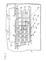
- a semiconductive substrate 10 such as silicon
- Two parallel elongate channel stops 11, 12 extend in a first direction and, in the present example, are highly doped regions of n-type conductivity formed in the top surface of the substrate 10.
- a first plurality of n-type channel stop fingers 14, 16, 18 extend in a second direction transverse to the first direction from the first channel stop 11 and are interlaced with and parallel to a second plurality of parallel n-type channel stop fingers 20, 22, 24 extending from the second channel stop 12.
- a first plurality of parallel elongate insulated electrodes 26, 28, 30, 32 extend in the first direction parallel to the channel stops 11, 12. The electrodes 26-32 are all formed at a first level above the top surface of the substrate 10.
- Charge transfer in the surface of the substrate 10 is effected in the serpentine path defined between the interlaced fingers 14-24 by means of a plurality of insulated electrode portions 34, 36, 38, 40, 42, 44, 46, 48, 50, 52, 54, 56 formed in a second level over the substrate 10.
- the first level electrodes 26-32 are formed in a lower level insulated polycrystalline silicon layer while the electrode portions 34-56 are formed in an upper level insulated polycrystalline silicon layer in a manner well known to those skilled in the art.
- Positive charge packets in the serpentine CCD of FIG. 1 are transferred sequentially beneath each of the electrode portions 34-56.
- a charge packet is first transferred beneath the electrode portion 34, secondly below the portion 36, then below the portion 38, etc., as indicated by the dashed-line arrows.
- alternate ones of the electrodes 26, 28, 30, 32 are connected to first and second complementary clock signals ⁇ 1, ⁇ 2 respectively, as indicated in FIG. 1.
- the electrode portions 34-56 are connected in alternate diagonal groups to the complementary clock signals ⁇ 1, ⁇ 2 by means of diagonally extending conductive portions 60, 62, 64, 66, 68, etc.
- the diagonal conductive portions 60-68 are each represented as a dashed line in FIG. 1 for simplicity.
- the diagonal group of electrode portions 34, 42, 50 is connected together by the conductive portion 64, the conductive portion 64 being connected to receive the clock signal ⁇ 2 .
- the conductive portion 64 is formed in the same upper level polysilicon layer that the electrode portions 34-56 are formed in.
- the diagonal group of electrode portions 44, 48, 52 is connected by means of the conductive portion 62 to receive the complementary clock signal ⁇ 1.
- the plurality of electrode portions 34-56 overlie the gaps between adjacent ones of the plurality of elongate parallel electrodes 26-32.
- Charge transfer occurs as follows. During a first time interval in which the clock signal ⁇ 1 is at a relatively low potential and the complementary clock signal ⁇ 2 is at a relatively high potential, the substrate surface potential beneath the electrode 26 is decreased so that a positive charge packet may be stored in the surface potential well (or "bucket") so formed beneath the electrode 26 between the two adjacent channel stop fingers 20, 22. Thereafter, the complementary clock signals ⁇ 1, ⁇ 2 change state and the clock signal ⁇ 2 is low while the clock signal ⁇ 1 is high so that the positive charge packet is attracted to flow beneath the electrode portion 34 and into an adjacent potential well formed beneath the electrode 28. The charge packet is now confined in the region beneath the electrode 28 between the adjacent channel stop fingers 14 and 22.
- the complementary clocks signals ⁇ 1, w 2 change state so that ⁇ 1 is now low. Accordingly, the positive charge packet is attracted from beneath the electrode 28 to flow under the electrode portion 36 to reside in a surface potential well formed beneath the electrode 30. The charge packet is still confined between the two channel stops 14, 22. Transfer of the positive charge packet continues beneath succeeding electrode portions 38, 40, 42, 44, etc., so that the charge packet follows the serpentine path indicated by the dashed-line arrows of FIG. 1.
- the direction of charge transfer is firmly established by the electrode arrangement illustrated in FIG. 1. Successive pairs of adjacent upper and lower level electrodes are connected alternately to receive one of the complementary clock signals ⁇ 1, W 2 .
- the formation of a surface potential well beneath a succeeding pair of one of the electrodes 26-32 and one of the electrode portions 34-56 is always acccompanied by the formation of a surface potential barrier beneath a preceeding pair of one of the electrodes 26-32 and one of the electrode portions 34-56.
- the clock signal ⁇ 1 is low while the clock signal W 2 is high, thus establishing a surface potential barrier beneath the electrode portion 34 and electrode 28 in the surface of the substrate 10 while establishing an attractive surface potential well beneath the electrode portion 36 and the electrode 30.
- a large number of charge packets may be transferred simultaneously beneath alternate ones of the electrode portions 34-56, without requiring a large number of electrical contacts.
- only four contacts are required to apply the complementary clock signals ⁇ 1, W 2 to the electrodes 26-32 and to the plurality of electrode portions 34-56.
- This feature is implemented by the diagonal connection portions 60-68 connecting each of the diagonal groups of electrode portions 34-56, each of the diagonal connection portions 60-68 requiring only one contact to connect it to receive one of the complementary clock signals ⁇ 1, W2.
- a principal advantage of the invention is that a given charge packet is transferred in the first direction parallel to the channel stops 11, 12 at a fraction (1/6 in the embodiment illustrated in FIG. 1) of the rate at which it is transferred in the second direction parallel to the channel stop fingers 14-22. Accordingly, the serpentine CCD of FIG. 1 operates at six times the clocking frequency of a prior art linear CCD serial register wherein charge is stepped only in the first direction.
- a TDI column of photodetectors 70, 72, 74, etc. may be disposed adjacent and parallel to the serpentine CCD of FIG. 1 on the substrate 10, each detector 70, 72, etc., being adjacent openings 12a, 12b in the channel stop 12.
- the transfer electrode 75 is connected to receive a clock signal ⁇ s which is synchronous with the clock signals ⁇ 1, ⁇ 2 .
- the TDI column of detectors 70-74 is optically scanned at the same rate that the charge is transferred in the serpentine CCD in the first direction parallel to the channel stop 12.
- the shaded areas correspond to buckets or CCD storage cells a, b, c, d which are formed simultaneously in the surface of the substrate 10 beneath the electrode 26 in a time interval during which the complementary clock signals ⁇ 1, ⁇ 2 are low and high, respectively.
- time delay and integration is achieved by scanning the field of view down the column of detectors 70, 72, 74 at the same rate that charge is.transferred from left to right between the buckets a, b, c, d. For example, the rate of charge transfer in the serpentine CCD of FIG.
- the serpentine CCD of FIG. 1 must be such that the same charge packet stored in the bucket b when the detector 70 views a particular pixel in the field of view must be transferred to the bucket d by the time the next detector 72 views the same pixel.
- the serpentine CCD of FIG. 1 the total number of CCD bits or buckets between the two input buckets b and d is six times the number which would be present in a simple linear CCD serial register. Therefore, the serpentine CCD must transfer charge at six times the velocity at which the TDI column of detectors 70-74 is scanned.
- an imager comprising the TDI column of detectors 70-74 and the serpentine CCD illustrated in FIG. 1 has six times the sampling rate of prior art CCD image sensors, a significant advantage.
- the number of electrodes 26-32 may be increased to any desired number by widening the serpentine CCD between the channel stops 11, 12 so that the sampling rate is proportionately increased to any desired number, which is theoretically unlimited. However, it is contemplated that various practical limitations (such as, for example, the area available on the CCD substrate) will be considered by a skilled worker in selecting the sampling rate.
- Another advantage of the invention is that the increase in the number of parallel electrodes 26-32 does not require that the capacity (or area) of each of the CCD buckets a, b, c, d be decreased. This is because the area of each CCD bucket is conserved by simply increasing the distance between the channel stops 11, 12. Thus, the sampling rate of the CCD imager may be increased without decreasing the capacity of each CCD bucket and the dynamic range of the device, thus virtually eliminating the trade-off which had previously existed in the prior art between dynamic range and sampling rate.
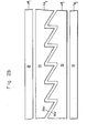
- FIG. 2a illustrates the preferred pattern of the channel stops 11, 12 and the interdigitated channel stop fingers 14-22.
- FIG. 2b illustrates the preferred pattern of the electrodes 26-32 formed in the lower level polysilicon layer.
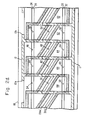
- FIG. 2c illustrates the preferred pattern of the combination of electrode portions 34-56 and diagonal connecting portions 60-68 formed in the upper polysilicon layer.
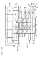
- FIG. 2d illustrates the overlay of the preferred patterns of FIGS. 2a, 2b and 2c.
- FIGS. 2a, 2b, 2c and 2d is essentially the same as the embodiment of FIG. 1 in fundamental structure.
- FIG. 2c illustrates that the diagonal connecting portions 60-68 of the preferred embodiment include each of the electrode portions 34-52 of FIG. 1 overlying the various gaps between the first level electrodes 28-32, as previously described.
- facing edges 28a, 30a of the first level electrodes 28, 30 extend along a straight line.
- facing edges 28a', 30a' extend in the same diagonal direction between each pair of adjacent channel stop fingers 14-24 as do the diagonal connecting portions 60-68.
- the diagonal connecting portions 60-68 can each assume the staircase configuration of the electrode 60' suggested in solid line in FIG. 1, in which case the facing electrode edges 28a, 30a are simply straight lines as illustrated in FIG. 1.
- the small linking portions 60" of the staircase electrode 60' of FIG. 1 must overlie and not extend beyond the underlying ones of the channel stop fingers 14-26, so that they must be quite thin. This can reduce the production yield of such devices.
- the facing edges of lower level electrodes underlying a diagonal electrode portion must themselves be diagonal.
- the facing edges of the lower level electrode pairs 30, 32 and 26, 28 are not diagonal. Accordingly, the diagonal electrode portions 60-68, as they extend over the latter facing electrode edges, become non-diagonal, or straight, and are terminated thereover.
- the serpentine CCD of FIG. 1 may be operated in an alternative mode 'as a 4-phase charge coupled device using a plurality of 4-phase clock signals ⁇ a, ⁇ b, ⁇ c, ⁇ d.
- alternate ones of the parallel electrodes 26-32 are connected to the clock signals ⁇ a , ⁇ b while alternate ones of the diagonal connecting portions 60-68 are connected to the clock signals ⁇ c , ⁇ d .
- the serpentine CCD of FIG. 1 may be used in devices other than CCD imagers.
- the serpentine CCD may be used as a means for performing series and parallel charge transfer in a CCD multiplexer.
- the serpentine CCD of FIG. 1 may be used in combination with a linear or meander channel CCD serial register as a delay line in a CCD signal processor.
- the meander channel CCD may be of the type disclosed in the above-referenced Parrish and Fletcher application.
- the delay line is illustrated in the simplified diagrams of FIGS. 3a and 3b, including a meander channel charge coupled device 100 formed on a semiconductive substrate 102 and a serpentine CCD 104 also formed on the substrate 102 in accordance with the present invention.
- the meander channel CCD 100 includes a plurality of interlaced channel stop fingers 106 formed in the substrate 102 and a pair of elongate electrodes 108, 110 overlying the substrate 102 and connected to receive the complementary clock signals ⁇ 1 , ⁇ 2 , respectively.
- the serpentine CCD 104 includes elements corresponding to those illustrated in FIGS. 2a, b, c, d, including the channel stops 11, 12, the interlaced channel stop fingers 14-24, parallel electrodes 26'-32' (with some differences discussed below) and the diagonal electrode portions 60-68.
- Openings 12a and 12b in the channel stop 12 permit the transfer of charge between the meander channel CCD 100 and the serpentine CCD 104 in the manner illustrated in FIG. 3a.
- Charge transfer from the meander channel CCD 100 into the serpentine CCD 104 occurs through the opening 12a under the control of the diagonal electrode portion 62.
- the diagonal electrode portions 60-68 extend over and beyond the parallel electrodes 28'-32' so as to overlie the gap between the meander channel electrode 110 and the parallel electrode 26' at the entrance 12a and the exit 12b.
- all of the facing electrode edges underlying the diagonal electrode portions 60-68 must themselves be diagonal. Accordingly, FIG. 3a shows that (in contrast with the embodiment of FIG. 2b) electrode edges 26a, 26b, 28a, 28b, 30a and 110a are all diagonal.
- the diagonal electrode portions 60-68 extend even further in FIG. 3a so as to overlie the gap between the CCD meander channel electrodes 108 and 110. This feature permits the diagonal electrode portions 60-68 to also control charge transfer in the meander channel CCD 100 in the manner of the interdigitated electrode fingers described in the above-referenced Parrish and Fletcher patent application.
- the charge admitted through the opening 12a is automatically returned through the opening 12b after a number of delays determined by the number of parallel electrodes 26'-32' in the serpentine CCD 104.
- the number of charge transfers occurring in the transverse direction of the serpentine CCD illustrated is six times the number of charge transfers occurring in the primary direction of the serpentine CCD. Accordingly, if the charge transfer between the openings 12a and 12b through the meander channel CCD 100 is considered to be one signal delay, then the charge transferred through the alternative path provided by the serpentine CCD 104 must go through seven delays, as indicated schematically in FIG. 3c. This may be confirmed by simply comparing the number of buckets between the openings 12a and 12b in the meander channel CCD 100 and the serpentine CCD 104.
- the serial register 100 may be a simple linear CCD serial register instead of a meander channel CCD.
- the number of parallel electrodes 28-32 in the serpentine CCD 104 of FIG. 3a may be increased to any desired number, the general result being illustrated in FIG. 4.
- the patterns of the channel stops 11, 12 and channel stop fingers 14, 16 and 22, 24 are the same as that illustrated in FIG. 2d except that the fingers are longer in FIG. 4.
- the pattern of the diagonal electrodes 6 0 -66 in FIG. 4 is also the same as in FIG. 2d except that they are longer.
- the pattern of the parallel electrodes 26, 28 in FIG. 4 is the same as in FIG . 2d.
- a plurality of sawtooth edge parallel electrodes 28' of the type illustrated in FIG. 3a are present in FIG. 4, this being a chief distinction of the embodiment of FIG. 4.
Landscapes
- Solid State Image Pick-Up Elements (AREA)
Applications Claiming Priority (2)
| Application Number | Priority Date | Filing Date | Title |
|---|---|---|---|
| US06/331,504 US4479201A (en) | 1981-12-17 | 1981-12-17 | Serpentine charge coupled device |
| US331504 | 1981-12-17 |
Publications (3)
| Publication Number | Publication Date |
|---|---|
| EP0082405A2 true EP0082405A2 (fr) | 1983-06-29 |
| EP0082405A3 EP0082405A3 (en) | 1986-01-02 |
| EP0082405B1 EP0082405B1 (fr) | 1989-09-06 |
Family
ID=23294246
Family Applications (1)
| Application Number | Title | Priority Date | Filing Date |
|---|---|---|---|
| EP82111335A Expired EP0082405B1 (fr) | 1981-12-17 | 1982-12-07 | Dispositif à charges couplées en forme de serpentin |
Country Status (6)
| Country | Link |
|---|---|
| US (1) | US4479201A (fr) |
| EP (1) | EP0082405B1 (fr) |
| JP (1) | JPS58151058A (fr) |
| AU (1) | AU563727B2 (fr) |
| DE (1) | DE3279932D1 (fr) |
| IL (1) | IL67320A0 (fr) |
Families Citing this family (2)
| Publication number | Priority date | Publication date | Assignee | Title |
|---|---|---|---|---|
| CA2135856A1 (fr) * | 1993-12-10 | 1995-06-11 | Steven Peter Allen | Dispositif de transmission de donnees adressable a faible consommation d'energie |
| US6459077B1 (en) * | 1998-09-15 | 2002-10-01 | Dalsa, Inc. | Bucket brigade TDI photodiode sensor |
Family Cites Families (6)
| Publication number | Priority date | Publication date | Assignee | Title |
|---|---|---|---|---|
| CA1023050A (fr) * | 1974-05-16 | 1977-12-20 | Western Electric Company, Incorporated | Filtres de ligne a retard pour transfert de charge |
| US3965462A (en) * | 1975-05-09 | 1976-06-22 | The United States Of America As Represented By The Secretary Of The Air Force | Serpentine charge-coupled-device memory circuit |
| JPS5332687A (en) * | 1976-09-07 | 1978-03-28 | Sony Corp | Charge transfer device |
| JPS5921189B2 (ja) * | 1978-10-30 | 1984-05-18 | 松下電子工業株式会社 | 電荷転送装置 |
| US4371885A (en) * | 1979-10-10 | 1983-02-01 | Hughes Aircraft Company | Charge coupled device improved meander channel serial register |
| US4380056A (en) * | 1980-10-10 | 1983-04-12 | Hughes Aircraft Company | Charge coupled device focal plane with serial register having interdigitated electrodes |
-
1981
- 1981-12-17 US US06/331,504 patent/US4479201A/en not_active Expired - Lifetime
-
1982
- 1982-11-22 IL IL67320A patent/IL67320A0/xx unknown
- 1982-12-07 EP EP82111335A patent/EP0082405B1/fr not_active Expired
- 1982-12-07 DE DE8282111335T patent/DE3279932D1/de not_active Expired
- 1982-12-14 AU AU91508/82A patent/AU563727B2/en not_active Ceased
- 1982-12-17 JP JP57221720A patent/JPS58151058A/ja active Granted
Also Published As
| Publication number | Publication date |
|---|---|
| DE3279932D1 (en) | 1989-10-12 |
| EP0082405B1 (fr) | 1989-09-06 |
| JPH0524663B2 (fr) | 1993-04-08 |
| IL67320A0 (en) | 1983-03-31 |
| AU9150882A (en) | 1983-06-23 |
| EP0082405A3 (en) | 1986-01-02 |
| US4479201A (en) | 1984-10-23 |
| AU563727B2 (en) | 1987-07-23 |
| JPS58151058A (ja) | 1983-09-08 |
Similar Documents
| Publication | Publication Date | Title |
|---|---|---|
| EP0313322B1 (fr) | Dispositif de prise d'images à semi-conducteur ayant plusieurs portions de transfert horizontal | |
| GB2026769A (en) | Charge transfer image sensors | |
| KR840002383A (ko) | 칼라 고체 촬상 장치 | |
| US4750042A (en) | Solid state image pickup element with dual horizontal transfer sections | |
| CA1096969A (fr) | Dispositif de transfert de charge | |
| EP0455801A1 (fr) | Capteur d'images | |
| US4870293A (en) | Extended-width CCD imager array capable of time-delay-integration operation | |
| US5040038A (en) | Solid-state image sensor | |
| US4639940A (en) | Charge coupled device with meander channel and elongated, straight, parallel gate electrodes | |
| US4757365A (en) | CCD image sensor with substantially identical integration regions | |
| US4720746A (en) | Frame transfer CCD area image sensor with improved horizontal resolution | |
| JPH0259673B2 (fr) | ||
| US4479201A (en) | Serpentine charge coupled device | |
| JPS625348B2 (fr) | ||
| US4141024A (en) | Solid state image sensing device | |
| JPH07161970A (ja) | 固体撮像装置 | |
| US4688066A (en) | Opposite direction multiple-phase clocking in adjacent CCD shift registers | |
| US5338948A (en) | Charge-coupled device with open gate structure | |
| EP0504852B1 (fr) | Dispositif à transfert de charges | |
| JPH04369268A (ja) | Ccd固体撮像素子 | |
| US4371885A (en) | Charge coupled device improved meander channel serial register | |
| JPH0337316B2 (fr) | ||
| US4277792A (en) | Piggyback readout stratified channel CCD | |
| JPH03114236A (ja) | 電荷転送装置 | |
| US4963956A (en) | Solid image pickup apparatus |
Legal Events
| Date | Code | Title | Description |
|---|---|---|---|
| PUAI | Public reference made under article 153(3) epc to a published international application that has entered the european phase |
Free format text: ORIGINAL CODE: 0009012 |
|
| AK | Designated contracting states |
Designated state(s): DE FR GB IT NL |
|
| PUAL | Search report despatched |
Free format text: ORIGINAL CODE: 0009013 |
|
| AK | Designated contracting states |
Designated state(s): DE FR GB IT NL |
|
| 17P | Request for examination filed |
Effective date: 19860619 |
|
| 17Q | First examination report despatched |
Effective date: 19870507 |
|
| RAP1 | Party data changed (applicant data changed or rights of an application transferred) |
Owner name: HUGHES AIRCRAFT COMPANY |
|
| GRAA | (expected) grant |
Free format text: ORIGINAL CODE: 0009210 |
|
| AK | Designated contracting states |
Kind code of ref document: B1 Designated state(s): DE FR GB IT NL |
|
| REF | Corresponds to: |
Ref document number: 3279932 Country of ref document: DE Date of ref document: 19891012 |
|
| ITF | It: translation for a ep patent filed | ||
| ET | Fr: translation filed | ||
| PLBE | No opposition filed within time limit |
Free format text: ORIGINAL CODE: 0009261 |
|
| STAA | Information on the status of an ep patent application or granted ep patent |
Free format text: STATUS: NO OPPOSITION FILED WITHIN TIME LIMIT |
|
| 26N | No opposition filed | ||
| PGFP | Annual fee paid to national office [announced via postgrant information from national office to epo] |
Ref country code: FR Payment date: 19911107 Year of fee payment: 10 |
|
| PGFP | Annual fee paid to national office [announced via postgrant information from national office to epo] |
Ref country code: GB Payment date: 19911114 Year of fee payment: 10 |
|
| PGFP | Annual fee paid to national office [announced via postgrant information from national office to epo] |
Ref country code: DE Payment date: 19911121 Year of fee payment: 10 |
|
| ITTA | It: last paid annual fee | ||
| PGFP | Annual fee paid to national office [announced via postgrant information from national office to epo] |
Ref country code: NL Payment date: 19911231 Year of fee payment: 10 |
|
| PG25 | Lapsed in a contracting state [announced via postgrant information from national office to epo] |
Ref country code: GB Effective date: 19921207 |
|
| PG25 | Lapsed in a contracting state [announced via postgrant information from national office to epo] |
Ref country code: NL Effective date: 19930701 |
|
| GBPC | Gb: european patent ceased through non-payment of renewal fee |
Effective date: 19921207 |
|
| NLV4 | Nl: lapsed or anulled due to non-payment of the annual fee | ||
| PG25 | Lapsed in a contracting state [announced via postgrant information from national office to epo] |
Ref country code: FR Effective date: 19930831 |
|
| PG25 | Lapsed in a contracting state [announced via postgrant information from national office to epo] |
Ref country code: DE Effective date: 19930901 |
|
| REG | Reference to a national code |
Ref country code: FR Ref legal event code: ST |