EP0082410A1 - Circuit pour supprimer des signaux dans des sections de lignes - Google Patents
Circuit pour supprimer des signaux dans des sections de lignes Download PDFInfo
- Publication number
- EP0082410A1 EP0082410A1 EP82111360A EP82111360A EP0082410A1 EP 0082410 A1 EP0082410 A1 EP 0082410A1 EP 82111360 A EP82111360 A EP 82111360A EP 82111360 A EP82111360 A EP 82111360A EP 0082410 A1 EP0082410 A1 EP 0082410A1
- Authority
- EP
- European Patent Office
- Prior art keywords
- signals
- line section
- circuit arrangement
- induction coil
- bridge
- Prior art date
- Legal status (The legal status is an assumption and is not a legal conclusion. Google has not performed a legal analysis and makes no representation as to the accuracy of the status listed.)
- Granted
Links
Images
Classifications
-
- H—ELECTRICITY
- H04—ELECTRIC COMMUNICATION TECHNIQUE
- H04B—TRANSMISSION
- H04B3/00—Line transmission systems
- H04B3/54—Systems for transmission via power distribution lines
- H04B3/56—Circuits for coupling, blocking, or by-passing of signals
-
- H—ELECTRICITY
- H04—ELECTRIC COMMUNICATION TECHNIQUE
- H04B—TRANSMISSION
- H04B2203/00—Indexing scheme relating to line transmission systems
- H04B2203/54—Aspects of powerline communications not already covered by H04B3/54 and its subgroups
- H04B2203/5404—Methods of transmitting or receiving signals via power distribution lines
- H04B2203/5425—Methods of transmitting or receiving signals via power distribution lines improving S/N by matching impedance, noise reduction, gain control
-
- H—ELECTRICITY
- H04—ELECTRIC COMMUNICATION TECHNIQUE
- H04B—TRANSMISSION
- H04B2203/00—Indexing scheme relating to line transmission systems
- H04B2203/54—Aspects of powerline communications not already covered by H04B3/54 and its subgroups
- H04B2203/5429—Applications for powerline communications
- H04B2203/5445—Local network
-
- H—ELECTRICITY
- H04—ELECTRIC COMMUNICATION TECHNIQUE
- H04B—TRANSMISSION
- H04B2203/00—Indexing scheme relating to line transmission systems
- H04B2203/54—Aspects of powerline communications not already covered by H04B3/54 and its subgroups
- H04B2203/5462—Systems for power line communications
- H04B2203/5483—Systems for power line communications using coupling circuits
Definitions
- the invention relates to a circuit arrangement for suppressing signals on line sections, an induction coil being inserted serially at the connection point of the line sections.
- signals are intentionally or unintentionally present on a part or section of this line, but for technical reasons they should be limited in their spread to this line section since they become undesirable or disruptive on further sections of this line Give effects cause.
- signals can, for example, be pure interference signals which arise from the switching of loads in the line section which is thus signal-laden.
- signals can also be, for example, frequency- or amplitude-modulated signals which are present in this line section in the broadest sense for communication purposes, for example in the context of intercom systems bound to this line section or also remote switching systems for influencing loads.
- Electrical lines are understood to mean all types of electrical lines, in particular also power supply lines, which are used, for example, in addition to their pure energy transfer function for purposes of communication and thus information transfer.
- induction coils of this type are relatively expensive since they have to have a high inductance in order to achieve a sufficiently high inductive resistance.
- the invention is based on the object of specifying a circuit arrangement of the type mentioned at the outset which reliably prevents the transfer of signals from one line section to another line section, induction coils of lower inductance being able to be used and a broadband shielding effect being achievable.
- an electrical compensation device which feeds a compensation signal compensating the signals at the junction of the induction coil with the line section on which the signals are to be suppressed.
- the signal present in a line section is thus already weakened when it passes through the induction coil.
- the remaining signal residue is then completely reduced to the value zero by a compensation signal fed in by the electrical compensation device.
- the compensation signal will therefore run in phase opposition to the residual signal.
- This compensation signal is determined by the compensation device from the signal present at the junction of the induction coil and the signal-carrying line section.
- the induction coil now only has to attenuate the signal to such an extent that the compensation device can suppress the residual signal, the induction coil can have a smaller inductance than in the prior art. Furthermore, a very broadband suppression of the signals is made possible, so that the elimination of broadband signals is also possible successfully.
- the compensation device is a Wheatstone bridge circuit that can be adjusted over a broadband range contains, in the first bridge branch of the induction coil and in the second, parallel bridge branch a capacitor is arranged, the line section having the interference signals via a third bridge branch with one connection of the capacitor and the line section to be kept free of the signals via a fourth bridge branch is connected to the other connection of the capacitor, that the compensation device further comprises a differential amplifier, the first input of which is connected to the one end of the bridge diagonal formed by the junction of the second and third bridge branches and the output of which is connected to the junction of the second and fourth bridge branches, and that the second input of the differential amplifier is connected to a reference voltage which has the value zero in the frequency range of the signals.
- the arrangement of the induction coil and the capacitor in parallel bridge branches leads to the fact that a broadband balanced bridge circuit is created, that is to say that the bridge circuit balanced for a specific frequency remains in the balanced state even when signals with a different frequency occur.
- the differential amplifier for which an operational amplifier is preferably used, is negative-coupled by the broadband-compensated bridge circuit and has to apply the power which is still required to compensate for the signal already weakened by the induction coil. There is therefore a correlation between the inductance of the induction coil and the output power of the differential amplifier in such a way that an increase in the output power of the differential amplifier becomes necessary as the inductance of the induction coil decreases.
- the components required for the compensation device are commercially available and can be obtained at low cost.
- the third and fourth bridge branches can each contain at least one ohmic resistor.
- a bridge circuit is obtained whose state of adjustment remains completely independent of the signal frequencies. This means that essentially all signals, regardless of their frequency, can be eliminated.
- the second input is connected via a parallel resonant circuit tuned to the line frequency and an ohmic resistor to the line section having the signals, and that the third and fourth bridge branches have only ohmic resistors.
- a very broadband compensation of the signals takes place, starting with signals which are significantly below the network frequency up to very high-frequency signals, signals in the vicinity of the network frequency also being compensated for.
- the differential amplifier Since the first input of the differential amplifier is fed from a superimposition of the mains frequency and the signals in the signal-laden mains line section, whereas the second input of the differential amplifier uses the parallel oscillating circuit tuned to the mains frequency to produce an ideal sinusoidal signal of the mains frequency, the differential amplifier enforces the connection point of the induction coil with the network line section to be kept free of the signals also an ideally sinusoidal signal, that is to say that this network line section no longer "feels" the signals present in the other network line section.
- a preferred embodiment of the invention for the case that the power line is used as a line is that by inserting further passive components in the third and fourth bridge branch, the bridge circuit is only adjusted for signals that are significantly above the line frequency and that the second input of the differential amplifier is connected to the neutral conductor of the network as a reference voltage source.
- capacitors can be arranged in series with the ohmic resistors. Due to the resulting RC elements, the broadband balanced bridge circuit for low signal frequencies is no longer in the balanced state, so that the compensation of signals of low frequency is suppressed and a parallel resonance circuit is no longer required to suppress the compensation of the mains frequency.
- the second input of the differential amplifier can be connected directly to the neutral conductor of the network.
- the differential amplifier can now be operated with lower supply voltages related to the neutral conductor, which simplifies the circuit or makes it possible to use a differential amplifier designed only for low voltage.
- the differential amplifier which is preferably designed as an operational amplifier, can also be replaced by a transistor. Such an arrangement behaves like a third-order low-pass filter.
- the transition from signals from the network line section with these signals to a subsequent network line section was suppressed.
- the transition of signals from the subsequent network line section which can also be signal-laden and which is referred to for this patent claim for reasons of a uniform nomenclature as "network line section to be kept free of the signals" was not suppressed in the already mentioned Signal-affected network line section, which for nomenclature reasons should apply to this claim as a "signal-affected network line section".
- this can be accomplished by arranging a further induction coil in series with the induction coil in the mains line section which is to be kept free of the signals, the induction coil's connection of which is also averted via the series connection of a capacitor and an ohmic resistor is connected to the first input of the differential amplifier.
- This circuit arrangement thus consists of two nested bridge circuits, one of which is in the above exemplary embodiments Bridge half connected to the first input of the differential amplifier, consisting of an induction coil and the series connection of capacitor and ohmic resistor, is provided a second time and is connected upstream of the induction coil. This prevents, for example, eavesdropping on network-connected intercoms from neighbors and the penetration of high-frequency network interference.
- this can be ruled out by supplying the output signal of the differential amplifier in phase opposition to the network line section having the signals. This reduces the load on the signal source arranged in the signal-carrying network line section, so that a signal of sufficient amplitude is available everywhere in this network line section. In a preferred embodiment, this can be done by connecting an inverting amplifier to the output of the differential amplifier via a resistor, the output signal of which is led via the series connection of a capacitor and a resistor to the mains line section having the signals.
- the problem with such a network used for communication purposes is that these signals also apply to network line sections in the other phases transfer.
- the signal-carrying network section of the one phase is connected by a circuit arrangement of the type mentioned in the preceding paragraph to the other network section of the same phase to be kept free of these signals.
- such a circuit arrangement can also be provided for this phase in order to couple the signals to a network line section of at least one further phase, the output signal of the differential amplifier of the circuit arrangement belonging to the one phase being conducted via a connecting line to the differential input of the reversing amplifier of the circuit arrangement assigned to the further phase is.
- the connecting line can contain a high-pass filter.
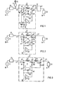
- 11 denotes a first line section, which represents the totality of the power lines installed in an apartment, for example the R phase.
- a second line section is designated by 12, which designates the network lines of the same phase which are located outside the home and are to be attributed to the power supply company.
- the network line impedance of the apartment is designated Z1
- the network line impedance of the line section located outside the apartment is designated Z2.
- a communication system for distributing information in which a transmitter T.
- the circuit arrangement S with dashed lines is provided.
- the two network line sections 11 and 12 are connected to one another by an induction coil L1 provided with a core.
- the induction coil L1 is located in the first branch 1 of a Wheatstone bridge circuit B, in the second bridge branch 2 of which a capacitor C1 is arranged in parallel.
- the connection a1 of the bridge branch 1 facing the signal-carrying network line branch 11 is connected via the third bridge branch 3 containing an ohmic resistor R1 to the terminal a2 of the second bridge branch facing the signal-carrying network line branch 11.
- connection a3 of the induction coil L1 connected to the mains line section 12 to be kept free of the signals is connected via the fourth bridge branch 4 containing an ohmic resistor R2 to the connection a4 of the bridge branch 2 facing the mains line section L2.
- This bridge circuit B consisting of the elements L1, C1, 'R1 and R2, represents a broadband-adjustable or broadband-compensated bridge circuit.
- the balancing condition for the bridge circuit in which the diagonal voltage V D occurring between the connections a2 and a3 becomes zero :
- the trimming condition is completely independent of frequency, so that the bridge circuit, once trimmed, remains in this trimmed state at all frequencies occurring at connections a1 and a4, in which the diagonal voltage V has the value zero.
- connection a2 corresponding to one connection of the bridge diagonal is led to the inverting input of an operational amplifier V1 used as a differential amplifier.
- the output of this operational amplifier V1 is connected to connection a4 of the bridge circuit B.
- the non-inverting connection of the operational amplifier V1 is connected to the one connection of the parallel resonance circuit P consisting of the capacitor C2 and the induction coil L2, the second connection of which is connected to the neutral conductor of the network.
- the non-inverting input of the operational amplifier V1 is connected to the mains line section 11 via the ohmic resistor R4. This resistor R4 determines the quality of the parallel resonance circuit P.
- the operational amplifier V1 thus represents a negative feedback network amplifier, the negative feedback branch being formed by the bridge circuit B.
- the parallel resonance circuit P is tuned to the mains frequency of 50 Hz. If the two mains line sections 11 and 12 are used not for the transmission of electrical energy but for the transmission of another AC voltage signal, the parallel resonance circuit must be tuned to the frequency of this AC voltage signal.
- this compensation circuit consisting of the bridge circuit B, the operational amplifier V1, the parallel resonance circuit P and the resistor R4 will be explained.
- the signals present on the power line section 11 would be in a frequency range of about 100 kHz.
- the capacitor C2 of the parallel resonance circuit P practically represents a short circuit, so that an ideal sinusoidal voltage with mains frequency is present at the non-inverting input of the operational amplifier V1.
- the sinusoidal mains voltage deformed by the signals present in the mains line section 11 is initially present (with fictitious ineffectiveness of V1).
- the negative feedback operational amplifier V1 now supplies such a current on the output side that the difference between the voltages present at its two inputs becomes zero. This is the case if the signal present at connection a2 of the bridge circuit B corresponds exactly to the ideal sinusoidal signal at the non-inverting input. Since the bridge circuit B is in the balanced state, in which the diagonal voltage V D occurring at the bridge diagonal between the terminals a2 and a3 becomes zero, an ideal sinusoidal voltage must also be removed at the terminal a3, free of the signals present in the first mains line section 11 to be available. Thus, under the action of the negative feedback operational amplifier V1, the signals of the power line section 11 that pass only weakly through the induction coil L1 are completely compensated. An analogous consideration applies to low-frequency signals of the mains line section 11, since they are short-circuited by the induction coil L2 of the parallel resonance circuit P.
- the full mains voltage occurs at the inputs of the operational amplifier V1, so that either an operational amplifier with corresponding voltage-proof inputs is to be used, or the operational amplifier by a supply related to the mains voltage voltage to feed.
- the induction coil L1 can therefore have a very small inductance, for example a few ⁇ H, the limit being given only by the power which the operational amplifier can provide and which is also directly dependent on the power of the signals to be compensated.
- an operational amplifier V1 of relatively low power there is no need to compensate for low-frequency signals which have the largest share of power. This can be done by bridging the capacitor C1 in the second bridge arm by an ohmic resistor. The compensation effect then occurs only from a lower cut-off frequency f, whereby is.
- the ohmic resistor R3 is shown in broken lines in FIG. 1.
- the electricity meter Z which is assigned to the apartment by the power supply company.
- FIGS. 2 to 4 the same reference numerals have been chosen for the components and structural units that correspond to FIG. 1. It should be emphasized that the circuit arrangement according to the invention, which is described in the following in connection with power lines, can also be used in connection with any electrical lines, even those which do not carry a signal a priori.
- the circuit arrangement according to the invention is outlined in dashed lines and identified by the reference symbol S '.
- the compensation of the low frequencies is suppressed.
- two additional RC elements R1C1 and R2C4 are formed in addition to the RC element C1R1 in the second bridge arm by inserting the capacitor C3 in the third bridge arm and the capacitor C4 in the fourth bridge arm of the bridge circuit B.
- the non-inverting input of the operational amplifier becomes V1 directly connected to the neutral conductor N of the electrical network, since suppression of the compensation of the network frequency by the parallel resonance circuit P is now dispensable.
- the operational amplifier V1 can now be operated with a low supply voltage related to the neutral conductor N of the network.
- the operational amplifier V1 can also be replaced by a transistor. It behaves like a third-order low-pass filter.
- the operational amplifier V1 forces - which applies high-frequency signals in the kHz range - in connection a3, in which the induction coil L1 is connected to the line section 12 to be kept free of these signals, the zero amplitude of these high-frequency signals, since the voltage is also zero at its non-inverting input is pending, and since the bridge circuit B is two-band, but only adjusted for the high frequency range mentioned.
- the compensation effect is suppressed in the range of low frequencies and thus also in the frequency range of the mains voltage.
- the circuit arrangement S ′′ which is framed by dashed lines, additionally has a further induction coil L11, which is connected upstream of the induction coil L1 with respect to the power line section 12.
- the connection a5 in which the additional induction coil L11 is connected to the power line section 12, is connected to the connection a2 and thus to the inverting input of the operational amplifier V1 via the ohmic resistor R11 and the capacitor C31 optionally arranged in series therewith.
- the inverting input of the operational amplifier V1 also "sees" the high-frequency signals arriving from the mains line section 12, so that these signals are also suppressed under point a3 under the negative feedback effect of the operational amplifier V1.
- the passage of these signals through the induction coil L1 into the power line section 11 is thus effectively suppressed.
- the signals from intercoms bound to the line section 12 can no longer be listened to in the line section 11.
- 1 bound communication system - be it an intercom or a remote switchgear -, when choosing an induction coil L1 of very small inductance there is a risk that the signal source T is too heavily loaded, so that considerable losses in intensity in the signal level occur, which the proper functioning of these communication systems can affect.
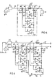
- the circuit arrangement S ''' comprises the circuit arrangement S' shown in FIG. 2, which, however, is supplemented here by further circuit-related measures.
- an inverting amplifier U is provided, which is connected to the output of the operational amplifier V1 via the ohmic resistor R5.
- the reversing amplifier U comprises an operational amplifier V2, the non-inverting input of which is connected to the neutral conductor of the electrical network, whereas the inverting input is connected to the ohmic resistor R5.
- the ohmic resistor R6 is arranged in the bridging branch of the operational amplifier V2.
- the output signal of the reversing amplifier U is led via the series circuit of an ohmic resistor R7 and a capacitor C5 to the connection a6, which is equivalent to the connection a1, of the signal-carrying line section 11.
- the compensation current supplied to the connection a3 is thus supplied in phase opposition to the connection a6, so that the signal source T coupled to the line section 11 in the context of a communication system is loaded only to a lesser extent.
- the resistor R1 which can be selected with a high resistance.
- the signal-carrying line section 11 and the line section 12 to be kept free from these signals belong to the network phase R.
- the signals carrying the information can be tapped not only from one network phase, but from all network phases.
- the transmission of the signals present in line section 11 of network phase R to network line section 11 'of phase S selected as an example is illustrated in FIG. 5.
- the two network line sections 11 and 12 of the network phase R are each connected to one another by a circuit arrangement illustrated in FIG. 4.
- the two line sections 11 'and 12' of the network phase S are connected to one another by an identical circuit arrangement, the elements which correspond to the aforementioned circuit arrangement being provided only with a reference symbol supplemented by an apostrophe.
- the output signal of the operational amplifier V1 which belongs to the circuit arrangement assigned to phase R, is connected via the connecting line 5 to the inverting input of the inverter U' Operational amplifier V2 ', which belongs to the circuit arrangement assigned to phase S, is supplied.
- the capacitor C6 and the ohmic resistor R9 are arranged in series as a high-pass filter.
Landscapes
- Engineering & Computer Science (AREA)
- Power Engineering (AREA)
- Computer Networks & Wireless Communication (AREA)
- Signal Processing (AREA)
- Cable Transmission Systems, Equalization Of Radio And Reduction Of Echo (AREA)
- Amplifiers (AREA)
Priority Applications (1)
| Application Number | Priority Date | Filing Date | Title |
|---|---|---|---|
| AT82111360T ATE18838T1 (de) | 1981-12-23 | 1982-12-08 | Schaltungsanordnung zur unterdrueckung von signalen auf leitungsabschnitten. |
Applications Claiming Priority (2)
| Application Number | Priority Date | Filing Date | Title |
|---|---|---|---|
| DE3151143 | 1981-12-23 | ||
| DE3151143A DE3151143C2 (de) | 1981-12-23 | 1981-12-23 | Schaltungsanordnung zur Unterdrückung von Signalen auf Leitungsabschnitten |
Publications (2)
| Publication Number | Publication Date |
|---|---|
| EP0082410A1 true EP0082410A1 (fr) | 1983-06-29 |
| EP0082410B1 EP0082410B1 (fr) | 1986-03-26 |
Family
ID=6149584
Family Applications (1)
| Application Number | Title | Priority Date | Filing Date |
|---|---|---|---|
| EP82111360A Expired EP0082410B1 (fr) | 1981-12-23 | 1982-12-08 | Circuit pour supprimer des signaux dans des sections de lignes |
Country Status (3)
| Country | Link |
|---|---|
| EP (1) | EP0082410B1 (fr) |
| AT (1) | ATE18838T1 (fr) |
| DE (2) | DE3151143C2 (fr) |
Cited By (1)
| Publication number | Priority date | Publication date | Assignee | Title |
|---|---|---|---|---|
| WO1993014550A1 (fr) * | 1992-01-10 | 1993-07-22 | Easy Shopping Ab | Agencement pour appareil electronique a protection par code |
Families Citing this family (1)
| Publication number | Priority date | Publication date | Assignee | Title |
|---|---|---|---|---|
| GB9616142D0 (en) | 1996-08-01 | 1996-09-11 | Northern Telecom Ltd | Distribution network |
Citations (6)
| Publication number | Priority date | Publication date | Assignee | Title |
|---|---|---|---|---|
| DE1147267B (de) * | 1960-08-30 | 1963-04-18 | Siemens Ag | Schaltungsanordnung zur traegerfrequenten UEbertragung von Nachrichtenzeichen ueber eine Hoch-spannungsleitung zwischen mindestens drei Stationen |
| GB1237029A (en) * | 1968-06-21 | 1971-06-30 | Baum Elektrophysik Gmbh | Circuit protecting telecommunication cables against fields of neighbouring power equipment |
| GB1271129A (en) * | 1968-11-07 | 1972-04-19 | Baum Elektrophysik Gmbh | Circuit or cable installation for reducing interference in telecommunication cables |
| DE2202896A1 (de) * | 1972-01-18 | 1973-07-19 | Licentia Gmbh | Schaltung zur unterdrueckung eines in einen elektrischen verstaerker eingestreuten stoersignals |
| DE2253861A1 (de) * | 1972-11-03 | 1974-05-09 | Wolfgang Dr Rer Nat Usinger | Verfahren und anordnung zum kompensieren von sinusfoermigen wechselspannungsueberlagerungen |
| GB2048622A (en) * | 1979-04-06 | 1980-12-10 | Electricity Council | Current reducing device |
Family Cites Families (1)
| Publication number | Priority date | Publication date | Assignee | Title |
|---|---|---|---|---|
| DE2952036C2 (de) * | 1979-12-22 | 1984-05-03 | Brown, Boveri & Cie Ag, 6800 Mannheim | Sperrfilter |
-
1981
- 1981-12-23 DE DE3151143A patent/DE3151143C2/de not_active Expired
-
1982
- 1982-12-08 DE DE8282111360T patent/DE3270174D1/de not_active Expired
- 1982-12-08 EP EP82111360A patent/EP0082410B1/fr not_active Expired
- 1982-12-08 AT AT82111360T patent/ATE18838T1/de not_active IP Right Cessation
Patent Citations (6)
| Publication number | Priority date | Publication date | Assignee | Title |
|---|---|---|---|---|
| DE1147267B (de) * | 1960-08-30 | 1963-04-18 | Siemens Ag | Schaltungsanordnung zur traegerfrequenten UEbertragung von Nachrichtenzeichen ueber eine Hoch-spannungsleitung zwischen mindestens drei Stationen |
| GB1237029A (en) * | 1968-06-21 | 1971-06-30 | Baum Elektrophysik Gmbh | Circuit protecting telecommunication cables against fields of neighbouring power equipment |
| GB1271129A (en) * | 1968-11-07 | 1972-04-19 | Baum Elektrophysik Gmbh | Circuit or cable installation for reducing interference in telecommunication cables |
| DE2202896A1 (de) * | 1972-01-18 | 1973-07-19 | Licentia Gmbh | Schaltung zur unterdrueckung eines in einen elektrischen verstaerker eingestreuten stoersignals |
| DE2253861A1 (de) * | 1972-11-03 | 1974-05-09 | Wolfgang Dr Rer Nat Usinger | Verfahren und anordnung zum kompensieren von sinusfoermigen wechselspannungsueberlagerungen |
| GB2048622A (en) * | 1979-04-06 | 1980-12-10 | Electricity Council | Current reducing device |
Cited By (1)
| Publication number | Priority date | Publication date | Assignee | Title |
|---|---|---|---|---|
| WO1993014550A1 (fr) * | 1992-01-10 | 1993-07-22 | Easy Shopping Ab | Agencement pour appareil electronique a protection par code |
Also Published As
| Publication number | Publication date |
|---|---|
| EP0082410B1 (fr) | 1986-03-26 |
| DE3151143C2 (de) | 1983-10-27 |
| DE3270174D1 (en) | 1986-04-30 |
| ATE18838T1 (de) | 1986-04-15 |
| DE3151143A1 (de) | 1983-07-14 |
Similar Documents
| Publication | Publication Date | Title |
|---|---|---|
| DE102014116594A1 (de) | Spannungssteuerschaltkreis für einen Feldgerätekoppler | |
| EP3378198B1 (fr) | Dispositifs et procédé de transmission d'un signal de communication et d'une puissance électrique entre des stations d'abonné d'un système de bus | |
| EP0212172B1 (fr) | Procédé et dispositif de compensation d'oscillations de courant | |
| DE102014109206B4 (de) | Sensorschnittstellensysteme und -verfahren | |
| EP1206846A1 (fr) | Dispositif de couplage pour systeme de transmission de donnees pour reseaux basse tension | |
| EP0004054B1 (fr) | Circuit d'égalisation automatique d'un signal | |
| EP0082410B1 (fr) | Circuit pour supprimer des signaux dans des sections de lignes | |
| DE4138065A1 (de) | Einrichtung zum uebertragen von daten und energie ueber eine leitung | |
| DE69803573T2 (de) | Netzfilterschaltungsanordnung | |
| EP0054811A1 (fr) | Egaliseur pour l'égalisation de signaux présentant une distorsion non-linéaire | |
| AT17225U1 (de) | Stromzähler zum Aufzeichnen des elektrischen Energieverbrauchs und ein Anpassungsmodul dafür | |
| EP0656696A2 (fr) | Dispositif de couplage d'énergie en courant continu à un bus à deux fils pour la transmission d'énergie et de données | |
| DE102008011582B4 (de) | Datenübertragungseinrichtung und Anlage | |
| DE2314418C3 (de) | Spulenloses kanonisches Bandfilter | |
| EP0923212A2 (fr) | Coupleur de bus | |
| WO2006105747A1 (fr) | Systeme electrique a plusieurs conducteurs pour la transmission symetrique de signaux, dote d'un element amortissant ou filtrant, et bus de transmission de donnees | |
| DE102006011595B4 (de) | Busankoppler für ein Bussystem, insbesondere EIB-Bussystem | |
| DE3033762A1 (de) | Entzerrerschaltung fuer nachrichtensignale | |
| EP0477660B1 (fr) | Circuit de reception d'informations transmises sur les lignes de puissance | |
| DE4412921C2 (de) | Verfahren und Schaltungsanordnung zur gleichzeitigen Übertragung von Daten und Hilfsenergie | |
| CH662021A5 (de) | Bandsperre mit einer hoeheren daempfung als 40 db zum sperren einer uebertragungsrichtung eines durch einen generator erzeugten hilfssignals in einem uebertragungssystem. | |
| DE102012205645A1 (de) | Übertragen von Daten über eine differentielle Datenleitung, insbesondere im Rahmen einer Fahrzeugkommunikation | |
| DE1110249B (de) | Gegentakt-Modulator | |
| DE102019133237B4 (de) | Störungsunterdrückung in einem Stromversorgungsnetz eines Fahrzeugs mittels steuerbarem Widerstand | |
| EP1816755A2 (fr) | Circuiterie pour transmettre des signaux de données depuis et/ou vers des appareils electromenager |
Legal Events
| Date | Code | Title | Description |
|---|---|---|---|
| PUAI | Public reference made under article 153(3) epc to a published international application that has entered the european phase |
Free format text: ORIGINAL CODE: 0009012 |
|
| AK | Designated contracting states |
Designated state(s): AT CH DE FR GB IT LI SE |
|
| 17P | Request for examination filed |
Effective date: 19831213 |
|
| ITF | It: translation for a ep patent filed | ||
| GRAA | (expected) grant |
Free format text: ORIGINAL CODE: 0009210 |
|
| AK | Designated contracting states |
Kind code of ref document: B1 Designated state(s): AT CH DE FR GB IT LI SE |
|
| REF | Corresponds to: |
Ref document number: 18838 Country of ref document: AT Date of ref document: 19860415 Kind code of ref document: T |
|
| REF | Corresponds to: |
Ref document number: 3270174 Country of ref document: DE Date of ref document: 19860430 |
|
| ET | Fr: translation filed | ||
| PGFP | Annual fee paid to national office [announced via postgrant information from national office to epo] |
Ref country code: AT Payment date: 19861128 Year of fee payment: 5 |
|
| PLBE | No opposition filed within time limit |
Free format text: ORIGINAL CODE: 0009261 |
|
| 26N | No opposition filed | ||
| ITTA | It: last paid annual fee | ||
| PGFP | Annual fee paid to national office [announced via postgrant information from national office to epo] |
Ref country code: DE Payment date: 19890223 Year of fee payment: 7 |
|
| PGFP | Annual fee paid to national office [announced via postgrant information from national office to epo] |
Ref country code: CH Payment date: 19890323 Year of fee payment: 7 |
|
| PG25 | Lapsed in a contracting state [announced via postgrant information from national office to epo] |
Ref country code: GB Effective date: 19891208 Ref country code: AT Effective date: 19891208 |
|
| PG25 | Lapsed in a contracting state [announced via postgrant information from national office to epo] |
Ref country code: SE Effective date: 19891209 |
|
| PG25 | Lapsed in a contracting state [announced via postgrant information from national office to epo] |
Ref country code: LI Effective date: 19891231 Ref country code: CH Effective date: 19891231 |
|
| GBPC | Gb: european patent ceased through non-payment of renewal fee | ||
| PG25 | Lapsed in a contracting state [announced via postgrant information from national office to epo] |
Ref country code: FR Effective date: 19900831 |
|
| REG | Reference to a national code |
Ref country code: CH Ref legal event code: PL |
|
| PG25 | Lapsed in a contracting state [announced via postgrant information from national office to epo] |
Ref country code: DE Effective date: 19900901 |
|
| REG | Reference to a national code |
Ref country code: FR Ref legal event code: ST |
|
| EUG | Se: european patent has lapsed |
Ref document number: 82111360.2 Effective date: 19900829 |