EP0083060A2 - Dispositif semi-conducteur comportant une diode de protection contre les surtensions - Google Patents
Dispositif semi-conducteur comportant une diode de protection contre les surtensions Download PDFInfo
- Publication number
- EP0083060A2 EP0083060A2 EP82111854A EP82111854A EP0083060A2 EP 0083060 A2 EP0083060 A2 EP 0083060A2 EP 82111854 A EP82111854 A EP 82111854A EP 82111854 A EP82111854 A EP 82111854A EP 0083060 A2 EP0083060 A2 EP 0083060A2
- Authority
- EP
- European Patent Office
- Prior art keywords
- region
- semiconductor substrate
- transistor
- protection diode
- base
- Prior art date
- Legal status (The legal status is an assumption and is not a legal conclusion. Google has not performed a legal analysis and makes no representation as to the accuracy of the status listed.)
- Granted
Links
Images


Classifications
-
- H—ELECTRICITY
- H10—SEMICONDUCTOR DEVICES; ELECTRIC SOLID-STATE DEVICES NOT OTHERWISE PROVIDED FOR
- H10D—INORGANIC ELECTRIC SEMICONDUCTOR DEVICES
- H10D8/00—Diodes
- H10D8/20—Breakdown diodes, e.g. avalanche diodes
- H10D8/25—Zener diodes
-
- H—ELECTRICITY
- H10—SEMICONDUCTOR DEVICES; ELECTRIC SOLID-STATE DEVICES NOT OTHERWISE PROVIDED FOR
- H10D—INORGANIC ELECTRIC SEMICONDUCTOR DEVICES
- H10D12/00—Bipolar devices controlled by the field effect, e.g. insulated-gate bipolar transistors [IGBT]
- H10D12/211—Gated diodes
-
- H—ELECTRICITY
- H10—SEMICONDUCTOR DEVICES; ELECTRIC SOLID-STATE DEVICES NOT OTHERWISE PROVIDED FOR
- H10D—INORGANIC ELECTRIC SEMICONDUCTOR DEVICES
- H10D89/00—Aspects of integrated devices not covered by groups H10D84/00 - H10D88/00
- H10D89/60—Integrated devices comprising arrangements for electrical or thermal protection, e.g. protection circuits against electrostatic discharge [ESD]
Definitions
- the present invention relates to a semiconductor device having a circuit which includes at least one transistor and, more particularly, to a semiconductor device having a transistor circuit of a high withstand voltage which includes an overvoltage protection diode with a controlled breakdown voltage.
- a combination of overvoltage protection diodes is used to protect the transistor elements. These protection diodes must be connected to the collector-base paths of the transistors on one chip. Furthermore, a breakdown voltage V zof the protection diode must be lower than a DC collector- to-emitter voltage (base open) V CEO .
- Such a protection diode is connected to the collector-base path of the transistor on one chip in the following manner.
- An impurity is deeply diffused from part of an inactive base region to a collector region of a high concentration, thereby determining the breakdown voltage V Z .
- an impurity is ion-implanted in part of the inactive base region to form a high-impurity region of the same conductivity type as that of the collector region, thus determining the breakdown voltage V Z .
- the protection diode of the type described above must be formed in a separate process from a process for forming a general transistor. Furthermore, in the case of an ignitor output circuit for an ignition control circuit of an internal combustion engine, the breakdown voltage of the protection diode must fall within a range of 360 V +10%. It is very difficult to set the breakdown voltage in the above range.
- the overvoltage protection diode built into the semiconductor device according to the present invention has a first region spaced apart from a second region in one major surface of the semiconductor substrate.
- the first region has a conductivity type opposite to that of the semiconductor substrate.
- the second region has the same conductivity as that of the semiconductor substrate and an impurity concentration higher than that of the substrate.
- a protection insulating film is formed to cover the entire surface including the first and second regions.
- a conductive film is then deposited on a portion of the protection insulating film so as to partially overlap the first and second regions. This conductive film then serves as a gate electrode.
- Fig. 1 shows an overvoltage protection diode formed in a semiconductor device.
- the semiconductor device has an n-type semiconductor substrate 10.
- a first region 11 which serves as a p-type anode region is formed on one major surface of the semiconductor substrate 10.
- a second region 12 which serves as a cathode region is also formed on the one major surface of the semiconductor substrate 10, spaced apart from the first region 11.
- the second region 12 has an impurity concentration higher than that of the first region 11 or an n +- type conductivity.
- An insulating film 13 such as a silicon oxide film is formed to cover the entire surface.
- a conductive film 14 is selectively formed on the insulating film 13. The conductive film 14 partially overlaps both first and second regions 11 and 12 through the insulating film 13, and is thus simultaneously surrounded by the first and second regions 11 and 12.
- the first region 11 functions as an anode electrode 15 and is connected as an anode to a lead wire.
- the conductive film 14 functions as a gate electrode and is connected as a gate to a lead wire.
- a conductive film 16 is then deposited on the other major surface of the semiconductor substrate 10 and is connected as a cathode to a lead wire.
- a power source E is connected between the gate and the anode, as shown in Fig. 2.
- a reverse-bias voltage is then applied to the anode.
- a gate voltage V G is set at 0 V.
- an inverted layer 17 is formed in a surface layer of the semiconductor substrate 10 beneath the conductive film 14 as the gate electrode.
- the inverted layer 17 extends between the first region 11 and the second region 12.
- a potential difference between the gate and the semiconductor substrate 10 in this state is defined as V T .
- a breakdown voltage V Z is always lower than an inherent withstand voltage of the semiconductor substrate 10. According to an experiment by the present inventors, the breakdown voltage V zi about one-third of the withstand voltage described above. Therefore, a transistor protection diode having the above-mentioned breakdown voltage can be suitably formed in a semiconductor device on a single chip.
- controllability of the breakdown voltage V may seem to depend upon a distance between the first region 11 and the second region 12.
- the inverted layer 17 is formed between the first region 11 and the second region 12 and is kept at a constant voltage. Therefore, the distance between the first and second regions 11 and 12 bears no relationship to the breakdown voltage, and may be determined only so as to obtain a required dielectric resistance or withstand voltage.
- the distance between the first and second regions 11 and 12 need not be precisely determined.
- the variation in the breakdown voltage V of this diode is about one-fifth of that of the conventional protection diode. This effect is called a buffer effect of the inverted layer.
- the active surface portion of the diode is shielded by the conductive film 14 through the insulating film 13. For this reason, influence of the external electric charge on the diode can be properly eliminated. Therefore, the breakdown voltage V z becomes stable, without any change over time.
- the semiconductor substrate 10 has an n-type conductivity and an impurity concentration of 1.5 x 10 14 atoms/cm 3 .
- the first region 11 comprises a p-type diffusion layer and has a surface concentration of 1 x 10 13 atoms/cm 3 .
- the depth of the diffusion layer is 30 ⁇ m.
- the second region 12 comprises an n-type diffusion layer and has a surface concentration of 2 x 10 19 atoms/cm 3 .
- the depth of the second region 12 is 18 ⁇ m.
- the insulating film 13 comprises a silicon oxide film (SiO 2 ) formed by phosphorus getter sputtering to a thickness of 4.0 ⁇ m.
- the conductive film 14 and the anode electrode 15 respectively comprise aluminum deposition films each having a thickness of 4.0 ⁇ m.
- the protection diode of the type described above When the protection diode of the type described above is used for protecting an output transistor circuit such as an ignitor of an internal combustion engine, the first region 11 is formed simultaneously with the formation of the base of the transistor element, whereas the second region 12 is formed when the emitter of the transistor element is formed.
- the field oxide film may be used as the insulating film 13.
- the conductive films or electrodes can be formed at the same time as the base and emitter electrodes of the transistor element are formed. In other words, when the protection diode is formed together with the transistor on the single chip, special steps for forming the protection diode are not required.
- the gate is directly connected by aluminum wiring to the first region 11. Furthermore, an inactive portion of the base region of the transistor formed in the semiconductor substrate 10 may also be used as the first region 11.
- a withstand voltage V BLUCK inherent in the semiconductor substrate is about 1,000 V.
- the collector- to-emitter voltage (base open) V CEO of the transistor having the base and emitter which are formed in the above-mentioned semiconductor substrate is about 400 V.
- the breakdown voltage V z of the protection diode shown in Fig. 1 is found to be given by the following equation: When a surface charge density Q SS of the insulating film 13 is given as 2 x 10 11 atoms/cm 3 , VT is given as about 50 V. Therefore, the breakdown voltage V Z turns out to be about 383 V.
- This breakdown voltage satisfies a rated range of 330 V ⁇ V z ⁇ V CEO for a protection Zener diode used for the output transistor circuit of the conventional ignitor. Furthermore, a change in the breakdown voltage V z falls within +5% due to the buffer effect of the inverted layer 17, which is not dependent upon the distance between the anode and the cathode.
- the stability of the breakdown voltage V z over time is considered.
- the active portion is shielded by the conductive film 14 from the external electric charge.
- the mobile electric charge within the insulating film 13 comprises positive electric charge such as Na + ions when getter sputtering is performed.
- the semiconductor substrate 10 has an n-type conductivity and the gate and the anode are commonly used with the base of the transistor. Therefore, the gate is kept at a negative potential. The positive electric charge described above is thus attracted to the gate and does not influence the active portion of the diode in the semiconductor substrate 10; thus a stable breakdown voltage V Z is constantly obtained.
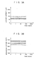
- Fig. 3A is a graph for explaining a leakage current I as a function of time when a BT test of the semiconductor device obtained in the above embodiment as a sample is made at a reverse-bias voltage of 300 V and at a high temperature of 170°C.
- Fig. 3B is a graph for explaining the breakdown voltage V as a function of time when the same test is performed under the same conditions as in Fig. 3A.
- the leakage current I and the breakdown voltage V z are stably maintained without variations.
- F ig. 4 shows the relationship between a current I AC and a voltage V AC between the anode and the cathode when the gate voltage V G in an equivalent circuit shown in Fig. 2 is changed using the test sample as described above.
- the breakdown voltage V is expressed by the following equation:
- the breakdown voltage V Z varies linearly with respect to the voltage V G.A between the gate and the anode, the breakdown voltage V can be arbitrarily set by setting the gate voltage.
- the diode thus breaks down with a minimum area of the depletion region 18 due to the buffer effect of the inverted layer 17. If the same operation area is given, it is confirmed by experiment that the operation resistance, or Zener diode, can be decreased to between half and one-fifth of that of a diffusion region obtained by diffusing an impurity in the conventional base region, or of that of an impurity-doped region obtained by ion-implanting an impurity in part of the inactive base region.
- FIGs. 5A and 5B show a transistor device including a protection diode.
- a semiconductor substrate 10 has an n-type conductivity and its impurity concentration is 1.4 x 10 14 atoms/cm 3 .
- An n +- type diffusion/collector region 20 is formed in the rear surface (the other major surface) of the semiconductor substrate 10.
- a p - type base region 21 is formed in the front surface (one major surface) of the semiconductor substrate 10.
- a first region 11 which corresponds to a p-type anode region of the diode is formed to surround the base region 21. The first region 11 is formed to be spaced apart from the base region 21. If parasitic capacitance need not be considered, the inactive region of the base region 21 may be also used as the first region 11.
- An n-type emitter region 22 is formed in the base region 21.
- a second region 12 which has an n-type conductivity is formed together with the emitter region 22 so. as to surround the first region 11.
- the second region 12 serves as the cathode region of the protection diode.
- the second region 12 is spaced apart from the first region 11 by a predetermined distance.
- An insulating film 13 which comprises a silicon oxide film is formed on the front surface of the semiconductor substrate 10.
- a conductive layer 14 is formed on the insulating layer 13 so as to partially overlap the first and second regions 11 and 12.
- the conductive film 14 is formed by deposition of aluminum together with a base electrode 23 and an emitter electrode 24 and is electrically connected to the first region 11.
- Fig. 6 shows an equivalent circuit of the transistor circuit shown in Figs. 5A and 5B.
- the semiconductor device of the type described above can be manufactured in the same manner as described above even if it has regions (including the semiconductor substrate) which are of opposite conductivity types to those of the regions shown in Figs. 5A and 5B.
- the diode tends to receive an effect of the positive mobile electric charge in the insulating film 13, as compared with the n-type semiconductor substrate.
- the anode and cathode regions may comprise buried epitaxial layers, respectively. Furthermore, the anode and cathode regions need not be formed simultaneously with the base and emitter of the transistor.
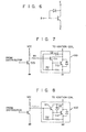
- Fig. 7 shows a Darlington circuit 100 which is arranged as an ignitor output circuit of the type described above.
- the Darlington circuit 100 has a drive transistor Trl and an output transistor Tr2 which are Darlington-connected.
- a protection diode D z is connected between the collector and base of the transistor Trl.
- a control signal to the transistor Trl is produced from the collector of a control transistor Tr3 and is supplied to the base of the transistor Trl through a resistor Ri.
- Figs. 9A and 9B show a semiconductor device having. the Darlington circuit 100 shown in Fig. 8.
- An n-type semiconductor substrate 10 has an impurity concentration of 1 x 10 14 to 2 x 10 14 atoms/cm 3 .
- An n +- type diffusion/collector region 20 is formed to cover the entire rear surface (the other major surface) of the semiconductor substrate 10.
- P-type base regions 21a and 21b of drive and output transistors are formed in the front surface (one major surface) of the semiconductor substrate 10.
- a first region 11 which has the same conductivity type as that of the base regions 21a and 21b is formed at the same time as the base regions 21a and 21b to surround them.
- the first region 11 functions as the anode region of the protection diode.
- n +- type second region 12 which is spaced apart from the first region 11 is formed to surround the first region 11.
- the second region 12 serves as the cathode region of the protection diode.
- the second region 12 is formed simultaneously with n-type emitter regions 22a and 22b.
- Phosphorus getter sputtering is performed to form an insulating film 13 to a thickness of 4 ⁇ m, using mainly silicon oxide (Si0 2 ), on the front surface of the semiconductor substrate 10 including the base regions 21a and 21b and the first and second regions 11 and 12.
- a conductive film 14 is formed on the insulating film 13 so as to partially overlap both first and second regions 11 and 12.
- the conductive film 14 is electrically connected to the first region 11 serving as the anode region, and is used as the anode electrode of the protection diode. At the same time, the conductive film 14 serves as a gate electrode of the protection diode by partially overlapping the second region 12 which serves as the cathode region of the protection diode. An aluminum base electrode 25 of the drive transistor, and an emitter electrode 26 and a collector electrode 27 of the output transistor are formed. The conductive film 14 which serves as the anode electrode of the protection diode is commonly connected to an emitter electrode 28 of the drive transistor and a base electrode 29 of the output transistor.
- the semiconductor device of the type described above has a Darlington circuit (Fig. 8) which is integrally formed on a single chip. Electrical characteristics of the Darlington transistor device including the protection diode are shown as follows.
- the withstand voltage of the semiconductor substrate 10 is about 1,000 V
- the withstand voltage between the collector and the emitter of the transistor is 450 V.
- the breakdown voltage at the base end portion which is surrounded by a guard ring can be more than 600 V by a cancelling effect of electric fields when the depletion region extending from the anode region of the protection diode overlaps the depletion region extending from the transistor. Therefore, this breakdown voltage is sufficiently large to satisfy the conventional requirement of the breakdown operation voltage (340 to 380 V) of the protection diode of the ignitor output circuit.
- the first region 11 which serves as the anode region of the protection diode can be formed simultaneously with the formation of the base regions 21a and 21b of the transistor.
- the second region 12 which serves as the cathode region can be formed simultaneously with the formation of the emitter regions 22a and 22b of the transistor.
- a portion of the insulating film 13 which is under the conductive film 14 as the gate electrode of the protection diode may be substituted by a field oxide film used for forming the transistor.
- the Darlington transistor circuit including the monolithic protection diode can be manufactured during the same process as is used for forming the conventional transistor.
- the conductive film 14 which is electrically connected to the first region 11 can be connected to the aluminum base electrode 25 of the drive transistor. In this case, the base electrode 29 of the output transistor is isolated from the conductive film 14.
- the Darlington circuit having a protection diode can be manufactured with the same process as is used for forming the transistor. Furthermore, regardless of the presence or absence of the pad portion, the diode can be formed together with the transistor on the same, single chip. Therefore, the number of externally connected components can be eliminated. Even if the protection diode is connected between the collector and the base of the output transistor (the base region of the output transistor does not have a pad portion), the chip size need not be increased.
Landscapes
- Bipolar Integrated Circuits (AREA)
- Bipolar Transistors (AREA)
Applications Claiming Priority (4)
| Application Number | Priority Date | Filing Date | Title |
|---|---|---|---|
| JP56215649A JPS58111369A (ja) | 1981-12-24 | 1981-12-24 | 半導体装置 |
| JP215649/81 | 1981-12-24 | ||
| JP17085/82 | 1982-02-05 | ||
| JP57017085A JPS58134467A (ja) | 1982-02-05 | 1982-02-05 | 半導体装置 |
Publications (4)
| Publication Number | Publication Date |
|---|---|
| EP0083060A2 true EP0083060A2 (fr) | 1983-07-06 |
| EP0083060A3 EP0083060A3 (en) | 1984-08-22 |
| EP0083060B1 EP0083060B1 (fr) | 1987-04-15 |
| EP0083060B2 EP0083060B2 (fr) | 1992-08-05 |
Family
ID=26353555
Family Applications (1)
| Application Number | Title | Priority Date | Filing Date |
|---|---|---|---|
| EP82111854A Expired EP0083060B2 (fr) | 1981-12-24 | 1982-12-21 | Dispositif semi-conducteur comportant une diode de protection contre les surtensions |
Country Status (3)
| Country | Link |
|---|---|
| US (1) | US5596217A (fr) |
| EP (1) | EP0083060B2 (fr) |
| DE (1) | DE3276091D1 (fr) |
Cited By (4)
| Publication number | Priority date | Publication date | Assignee | Title |
|---|---|---|---|---|
| DE3411878A1 (de) * | 1983-03-31 | 1984-10-04 | Nippondenso Co., Ltd., Kariya, Aichi | Halbleiterschaltkreis mit ueberspannungs-schutzeinrichtung |
| EP0408124A3 (en) * | 1989-07-11 | 1991-03-20 | Sgs-Thomson Microelectronics S.R.L. | Circuit for protection against negative overvoltages across the power supply of an integrated circuit comprising a power device with related control circuit |
| US5210675A (en) * | 1989-07-11 | 1993-05-11 | Sgs-Thomson Microelectronics S.R.L. | Circuit for protection against negative overvoltages across the power supply of an integrated circuit comprising a power device with related control circuit |
| EP0746031A3 (fr) * | 1995-05-31 | 2000-06-14 | Nec Corporation | Dispositif semi-conducteur du type silicium sur isolant |
Families Citing this family (4)
| Publication number | Priority date | Publication date | Assignee | Title |
|---|---|---|---|---|
| US6380570B1 (en) * | 2000-04-21 | 2002-04-30 | International Business Machines Corporation | Gate overvoltage control networks |
| US7265740B2 (en) * | 2002-08-30 | 2007-09-04 | Toshiba Matsushita Display Technology Co., Ltd. | Suppression of leakage current in image acquisition |
| KR101043737B1 (ko) * | 2007-02-15 | 2011-06-24 | 주식회사 하이닉스반도체 | 정전기 방전 보호 소자 |
| US20090118984A1 (en) * | 2007-11-05 | 2009-05-07 | Xiuyu Che | Ignition Method with Energy Conservation and Environmental Protection for Gasoline Engine |
Family Cites Families (9)
| Publication number | Priority date | Publication date | Assignee | Title |
|---|---|---|---|---|
| NL6904619A (fr) * | 1969-03-25 | 1970-09-29 | ||
| US3648340A (en) * | 1969-08-11 | 1972-03-14 | Gen Motors Corp | Hybrid solid-state voltage-variable tuning capacitor |
| JPS50137478A (fr) * | 1974-04-18 | 1975-10-31 | ||
| JPS573225B2 (fr) * | 1974-08-19 | 1982-01-20 | ||
| US4037140A (en) * | 1976-04-14 | 1977-07-19 | Rca Corporation | Protection circuit for insulated-gate field-effect transistors (IGFETS) |
| JPS5556656A (en) * | 1978-10-23 | 1980-04-25 | Nec Corp | Semiconductor device |
| JPS5580352A (en) * | 1978-12-12 | 1980-06-17 | Fuji Electric Co Ltd | Transistor with high breakdown voltage |
| JPS55125678A (en) * | 1979-03-23 | 1980-09-27 | Nec Corp | Zener diode |
| DE3117804A1 (de) * | 1981-05-06 | 1982-11-25 | Robert Bosch Gmbh, 7000 Stuttgart | "planare transistorstruktur" |
-
1982
- 1982-12-21 DE DE8282111854T patent/DE3276091D1/de not_active Expired
- 1982-12-21 EP EP82111854A patent/EP0083060B2/fr not_active Expired
-
1989
- 1989-09-14 US US07/407,157 patent/US5596217A/en not_active Expired - Lifetime
Cited By (4)
| Publication number | Priority date | Publication date | Assignee | Title |
|---|---|---|---|---|
| DE3411878A1 (de) * | 1983-03-31 | 1984-10-04 | Nippondenso Co., Ltd., Kariya, Aichi | Halbleiterschaltkreis mit ueberspannungs-schutzeinrichtung |
| EP0408124A3 (en) * | 1989-07-11 | 1991-03-20 | Sgs-Thomson Microelectronics S.R.L. | Circuit for protection against negative overvoltages across the power supply of an integrated circuit comprising a power device with related control circuit |
| US5210675A (en) * | 1989-07-11 | 1993-05-11 | Sgs-Thomson Microelectronics S.R.L. | Circuit for protection against negative overvoltages across the power supply of an integrated circuit comprising a power device with related control circuit |
| EP0746031A3 (fr) * | 1995-05-31 | 2000-06-14 | Nec Corporation | Dispositif semi-conducteur du type silicium sur isolant |
Also Published As
| Publication number | Publication date |
|---|---|
| EP0083060A3 (en) | 1984-08-22 |
| EP0083060B2 (fr) | 1992-08-05 |
| DE3276091D1 (en) | 1987-05-21 |
| US5596217A (en) | 1997-01-21 |
| EP0083060B1 (fr) | 1987-04-15 |
Similar Documents
| Publication | Publication Date | Title |
|---|---|---|
| US4595941A (en) | Protection circuit for integrated circuit devices | |
| US4044373A (en) | IGFET with gate protection diode and antiparasitic isolation means | |
| US5072273A (en) | Low trigger voltage SCR protection device and structure | |
| US5932916A (en) | Electrostatic discharge protection circuit | |
| US4697199A (en) | Semiconductor protection device having a bipolar transistor and an auxiliary field effect transistor | |
| US4786956A (en) | Input protection device for integrated circuits | |
| US6268628B1 (en) | Depletion type MOS semiconductor device and MOS power IC | |
| US3739238A (en) | Semiconductor device with a field effect transistor | |
| US3999212A (en) | Field effect semiconductor device having a protective diode | |
| US4631562A (en) | Zener diode structure | |
| US4937639A (en) | Input protector device for semiconductor device | |
| KR20030096026A (ko) | 정전기 방전 보호 소자 | |
| EP0103306B1 (fr) | Dispositif semi-conducteur de protection | |
| US6046476A (en) | SOI input protection circuit | |
| US5895958A (en) | Input protection circuit for use in semiconductor device having an improved electrostatic breakdown voltage | |
| EP0083060B1 (fr) | Dispositif semi-conducteur comportant une diode de protection contre les surtensions | |
| US6373672B1 (en) | Static and monolithic current limiter and circuit-breaker component | |
| US4672402A (en) | Semiconductor circuit device including an overvoltage protection element | |
| US5109266A (en) | Semiconductor integrated circuit device having high breakdown-voltage to applied voltage | |
| US4651178A (en) | Dual inverse zener diode with buried junctions | |
| US4649414A (en) | PNPN semiconductor switches | |
| US6127723A (en) | Integrated device in an emitter-switching configuration | |
| EP0472592B1 (fr) | Structure et dispositif de protection muni d'un redresseur au silicium commande a basse tension de declenchement | |
| US4438449A (en) | Field effect semiconductor device having a protective diode with reduced internal resistance | |
| JPH01140757A (ja) | 半導体入力保護装置 |
Legal Events
| Date | Code | Title | Description |
|---|---|---|---|
| PUAI | Public reference made under article 153(3) epc to a published international application that has entered the european phase |
Free format text: ORIGINAL CODE: 0009012 |
|
| AK | Designated contracting states |
Designated state(s): DE FR GB |
|
| PUAL | Search report despatched |
Free format text: ORIGINAL CODE: 0009013 |
|
| AK | Designated contracting states |
Designated state(s): DE FR GB |
|
| 17P | Request for examination filed |
Effective date: 19841013 |
|
| 17Q | First examination report despatched |
Effective date: 19860123 |
|
| GRAA | (expected) grant |
Free format text: ORIGINAL CODE: 0009210 |
|
| AK | Designated contracting states |
Kind code of ref document: B1 Designated state(s): DE FR GB |
|
| REF | Corresponds to: |
Ref document number: 3276091 Country of ref document: DE Date of ref document: 19870521 |
|
| ET | Fr: translation filed | ||
| PLBI | Opposition filed |
Free format text: ORIGINAL CODE: 0009260 |
|
| 26 | Opposition filed |
Opponent name: ROBERT BOSCH GMBH Effective date: 19880111 |
|
| PUAH | Patent maintained in amended form |
Free format text: ORIGINAL CODE: 0009272 |
|
| STAA | Information on the status of an ep patent application or granted ep patent |
Free format text: STATUS: PATENT MAINTAINED AS AMENDED |
|
| 27A | Patent maintained in amended form |
Effective date: 19920805 |
|
| AK | Designated contracting states |
Kind code of ref document: B2 Designated state(s): DE FR GB |
|
| ET3 | Fr: translation filed ** decision concerning opposition | ||
| PGFP | Annual fee paid to national office [announced via postgrant information from national office to epo] |
Ref country code: FR Payment date: 20011212 Year of fee payment: 20 |
|
| PGFP | Annual fee paid to national office [announced via postgrant information from national office to epo] |
Ref country code: GB Payment date: 20011219 Year of fee payment: 20 |
|
| REG | Reference to a national code |
Ref country code: GB Ref legal event code: IF02 |
|
| PGFP | Annual fee paid to national office [announced via postgrant information from national office to epo] |
Ref country code: DE Payment date: 20020109 Year of fee payment: 20 |
|
| PG25 | Lapsed in a contracting state [announced via postgrant information from national office to epo] |
Ref country code: GB Free format text: LAPSE BECAUSE OF EXPIRATION OF PROTECTION Effective date: 20021220 |
|
| REG | Reference to a national code |
Ref country code: GB Ref legal event code: PE20 Effective date: 20021220 |