EP0083181A2 - Intergrierte logische Schaltung - Google Patents
Intergrierte logische Schaltung Download PDFInfo
- Publication number
- EP0083181A2 EP0083181A2 EP82306768A EP82306768A EP0083181A2 EP 0083181 A2 EP0083181 A2 EP 0083181A2 EP 82306768 A EP82306768 A EP 82306768A EP 82306768 A EP82306768 A EP 82306768A EP 0083181 A2 EP0083181 A2 EP 0083181A2
- Authority
- EP
- European Patent Office
- Prior art keywords
- gate
- field effect
- effect transistors
- fet
- normally
- Prior art date
- Legal status (The legal status is an assumption and is not a legal conclusion. Google has not performed a legal analysis and makes no representation as to the accuracy of the status listed.)
- Granted
Links
- 230000005669 field effect Effects 0.000 claims description 21
- 239000002184 metal Substances 0.000 claims description 4
- 229910001218 Gallium arsenide Inorganic materials 0.000 description 13
- 238000010586 diagram Methods 0.000 description 8
- 239000007787 solid Substances 0.000 description 5
- 229910052710 silicon Inorganic materials 0.000 description 2
- XUIMIQQOPSSXEZ-UHFFFAOYSA-N Silicon Chemical compound [Si] XUIMIQQOPSSXEZ-UHFFFAOYSA-N 0.000 description 1
- 150000001875 compounds Chemical class 0.000 description 1
- 230000000694 effects Effects 0.000 description 1
- 230000004941 influx Effects 0.000 description 1
- 238000004519 manufacturing process Methods 0.000 description 1
- 230000004048 modification Effects 0.000 description 1
- 238000012986 modification Methods 0.000 description 1
- 238000009877 rendering Methods 0.000 description 1
- 239000010703 silicon Substances 0.000 description 1
- 239000000758 substrate Substances 0.000 description 1
Images

Classifications
-
- H—ELECTRICITY
- H03—ELECTRONIC CIRCUITRY
- H03K—PULSE TECHNIQUE
- H03K19/00—Logic circuits, i.e. having at least two inputs acting on one output; Inverting circuits
- H03K19/02—Logic circuits, i.e. having at least two inputs acting on one output; Inverting circuits using specified components
- H03K19/08—Logic circuits, i.e. having at least two inputs acting on one output; Inverting circuits using specified components using semiconductor devices
- H03K19/094—Logic circuits, i.e. having at least two inputs acting on one output; Inverting circuits using specified components using semiconductor devices using field-effect transistors
- H03K19/09403—Logic circuits, i.e. having at least two inputs acting on one output; Inverting circuits using specified components using semiconductor devices using field-effect transistors using junction field-effect transistors
- H03K19/09407—Logic circuits, i.e. having at least two inputs acting on one output; Inverting circuits using specified components using semiconductor devices using field-effect transistors using junction field-effect transistors of the same canal type
-
- H—ELECTRICITY
- H03—ELECTRONIC CIRCUITRY
- H03K—PULSE TECHNIQUE
- H03K19/00—Logic circuits, i.e. having at least two inputs acting on one output; Inverting circuits
- H03K19/02—Logic circuits, i.e. having at least two inputs acting on one output; Inverting circuits using specified components
- H03K19/08—Logic circuits, i.e. having at least two inputs acting on one output; Inverting circuits using specified components using semiconductor devices
- H03K19/094—Logic circuits, i.e. having at least two inputs acting on one output; Inverting circuits using specified components using semiconductor devices using field-effect transistors
- H03K19/0952—Logic circuits, i.e. having at least two inputs acting on one output; Inverting circuits using specified components using semiconductor devices using field-effect transistors using Schottky type FET MESFET
Definitions
- This invention relates to an integrated logic circuit employing normally-off type field effect transistors such as metal Schottky-barrier-gate FET's (Si MESFET's and compound MESFET's) and junction gate FET's (JFET's).
- normally-off type field effect transistors such as metal Schottky-barrier-gate FET's (Si MESFET's and compound MESFET's) and junction gate FET's (JFET's).
- GaAs FET's An integrated logic circuit employing GaAs FET's is receiving a great deal of attention as a high-speed data processing IC.
- Basic logic gate circuits employing GaAs FET's include those which use normally-on type GaAs FET's and those which use normally-off type GaAs FET's. Although circuits of the latter category involve difficult manufacturing procedures, they can be realized by the simplest configuration. The latter logic circuits are therefore expected to realize an highly integrated logic circuit employing GaAs FET's.
- An integrated logic circuit employing GaAs FET's generally comprises metal Schottky-barrier-gate FET's or Schottky-gate FET's (to be referred to as MESFET's hereinafter), or junction gate FET's (to be referred to as JFET's hereinafter).
- MESFET's Schottky-barrier-gate FET's
- JFET's junction gate FET's
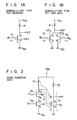
- a forward current may flow from the gate tc a grounded source electrode. Accordingly the gate potential is clamped to the voltage determined by the rise voltage of this forward current (about 0.7 V in the case of a MESFET and about 1.2 V in the case of a JFET). If a NAND gate constructed by normally-off type MESFET's, Si MESFET's or JFET's, the following problem is encountered. Fig.
- NAND gate 2 shows a NAND gate consisting of normally-off type FET's Ql and Q2 and a resistor Rl; and an inverter consisting of an FET Q3 and a resistor R2, this inverter being connected to receive an output from the. NAND gate.
- the NAND gate shown in Fig. 2 when the input logic level of the gate input terminal INl of the FET Ql is LOW ("0") to turn it off, and when the logic level of the gate input terminal IN2 of the FET Q2 at the side of a power supply VDD is HIGH (“1") to turn it on, a forward current Il of the gate input terminal IN1 is not allowed to flow into the source of the FET Ql since it turns OFF.
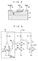
- the MESFET comprises, as shown in Fig. 3, a gate electrode 16 for defining a Schottky contact 14 with the surface of an active layer 12 formed on a substrate 10, and a source electrode 18 and a drain electrode 20 for defining ohmic contact with the layer 12. Since the active layer 12 is very thin, a considerably large series resistance Rs is present, as schematically shown in Fig. 3. Therefore, in the state of the circuit shown in Fig. 2, the effective source potential of the FET Q3 is given by Rs.(Il + 12 + 13).
- the potential of the source S3 of the FET Q3 (inverter) receiving signals from the output terminal of the NAND gate is further increased by the voltage defined by Rs-11, compared with in the case of sole NOR gate or inverter, rendering the holding of the "0" level difficult. For this reason, a NAND gate employing normally-off type GaAs FET's has not be used in an integrated logic circuit.
- an integrated logic circuit which comprises:
- the problem can be solved which is usually encountered when normally-off type field effect transistors are integrated to construct a NAND gate or an AND gate. That is, an undesirable increase in the logic level of a given stage due to the influx of the current from a previous stage can be prevented. Accordingly, stable logic operation of the IC is ensured.
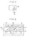
- Fic. 8 shows a circuit diagram of a frequency divider circuit employing AND/NOR gates according to the present invention.
- Fig. 4 shows a circuit diagram of one p referrec embodiment wnere the state of current flow in an integrated logic circuit employing GaAs FET's is illustrated comparing with Fig. 2.
- the GaAs integrated logic circuit is constructed by a NOR gate 30, one gate of which is additionally connected to the conventional NAND/INVERTER as shown in Fig. 2.
- This NOR gate is constructed by a fourth FET Q4 of MESFET or JFET type, a fifth FET Q5, and a resistor R3, the source-to-drain current path of the fourth FET Q4 being connected parallel to that of the fifth FET Q5, and the resistor R3 being connected between one power supply terminal VDD and the node made between the drains D4 and D5 of the FET's Q4 and Q5, respectively.
- the NAND aate of the normally-off type logic IC can be realized by constructing the circuitry as shown in Fi g. 4. That is, the gate of the second FET Q2 particially constructing the NAND gate, which is not connected to the ground (VSS), is connected to the gate of the fourth FET Q4 particially constructing the NOR gate, the source of the last-mentioned FET being connected to the ground ( V SS) so as to by-pass the gate-forward current of the FET (Q2) through the gate-to-source path of the FET Q4.
- a plurality of input terminals of the NAND gate (or the AND/NOR gate) in a normally-off type logic IC are not mutually equivalent in view of the gate connection, and those of the FET's constructing the NAND or AND/NOR gate at the ground side must be distinquished from those of the other FET's.
- Representation of the NAND gate as shown in Fig. 5(A) must therefore be given, for example, as shown in Fig. 5(B) in order to distinguish between the two input gates.
- the input terminal IN1,(indicated by a solid "dot" at the side of the one power supply terminal VDD (not the side of the around) is necessarily connected in parallel with the input terminal of other NOR gate (not shown) or the inverter.
- a parallel multiplier is widely adopted as a basic logic arithmetic device and generally is categorized to a full adder and a half adder.
- the half adder may be easily obtained from a combination of NOR gates and inverters, the full adder would have a considerably complex configuration if it were constructed by only these two types of logic gates. So if an AND/NOR gate can be used as one of modifica- rions of the NAND gate, the full adder may be obtained with a smaller number of NAND (i.e., AND/NOR) gates as shown in Fig. 6. Referring to Fig. 6, all gates 41 to 47 are constructed by normally-off type MFSFET's .
- Input signals to be added together are supplied to two input terminals X and Y of a first NOR gate 41.
- the output terminal of this NOR gate 41 is connected to one AND input terminal of a first AND/NOR gate 42.
- the other AND input terminal of the first AND/NOR gate 42 is connected to one input terminal of a second NOR gate 43, which also receives a carry signal.
- the output terminal of the second NOR gate 43 is connected to one input terminal of a NOR gate of a second AND/NOR gate 45.
- a carry bit signal is produced from an output terminal C' of the second AND/NOR gate 45.
- One AND input terminal of a third AND/NOR gate 47 is connected to the input terminal of an inverter 44.
- the summation resulted from the previous stage (not shown) is supplied to a common connection terminal K.
- the other AND input terminal of the third AND/NOR gate 47 is connected to one input terminal of a third NOR gate 46, as well as to one AND input terminal of the second AND/NOR gate 45 and further to the output terminal of the first AND/NOR gate 42.
- the summation resulted from this full adder is produced from an output terminal S of the third AND/NOR gate 47.
- both AND input terminals of the first and third AND/NOR gates 42 and 47 are connected in parallel with the input terminal of the separate NOR gates 43 and.46 respectively. Under this condition, the previously explained forward current may not flow from the present stage to the next stage. However, one of the AND input terminals of the second AND/NOR gate 45 is connected in parallel with the NOP gate 46, while the other one is not.
- the present invention provides advantages in this condition. More specifically, the one AND input terminal (indicated by a solid "dot") of the second AND/NOR gate 45 at tne side of the power supply is selected to be connected in parallel with the NOR gate 46 with respect to the ground.
- the forward current may be passed to the second NOR gate 46, so that the overall circuit may operate stably.
- the forward current shall flow from the output terminal C' of the second AND/NOR gate 45 to the next stage (not shown), so that its logic level "0" will rise to from 0.2 to 0.3 V, which is approximately 0.1 V higher than the general logic level "0" voltage (g 0.1 V), resulting in error operation.
- the one AND input terminal (indicated by a solid "dot") of the AND/NOR gate 45 at the side of the power supply is connected to the NOR gate 46 constructing its own IC to achieve the effect of the present invention.
- the present invention may be practiced by adding an inverter independently which has no relation to the original logic function of the IC. For example, as shown in Fig.
- a flip-flop * logic circuit constituted as a frequency divider that employs two normally-off type AND/NOR gates according to the present invention.
- a flip-flop logic circuit 60 comprises a master portion 62 and a slave portion 64.
- each one input terminal (indicated by a solid "dot") of AND gates 66 and 68 belonging to the master portion 62 is necessarily connected to the corresponding one input terminal of each of NOR gates 72 and 74 belonging to the slave portion 64 respectively.
- each one input terminal (indicated by solid "dot") of AND gate 76 and 78 is necessary to be connected to the corresponding input terminal of each of NOR gates 82 and 84 respectively.
- a clock signal (T) is usually supplied to an input IN3 of the master portion 62 and an inverted clock signal (T) is to an input IN4 of the slave portion 64. Accordingly, the aforementioned conventional drawbacks of the normally-off type NAND gate can be avoided by the circuit in Fig. 8.
- the NAND gate has only two input terminals.
- the NAND gate may have 3 or more input terminals.
- the input terminals of the respective gates excluding those of the FET whose source is grounded may be connected to corresponding separate NOR gates.
Landscapes
- Engineering & Computer Science (AREA)
- Power Engineering (AREA)
- Physics & Mathematics (AREA)
- Computer Hardware Design (AREA)
- Computing Systems (AREA)
- General Engineering & Computer Science (AREA)
- Mathematical Physics (AREA)
- Logic Circuits (AREA)
Applications Claiming Priority (2)
| Application Number | Priority Date | Filing Date | Title |
|---|---|---|---|
| JP56214911A JPS58114528A (ja) | 1981-12-26 | 1981-12-26 | GaAs論理集積回路 |
| JP214911/81 | 1981-12-26 |
Publications (3)
| Publication Number | Publication Date |
|---|---|
| EP0083181A2 true EP0083181A2 (de) | 1983-07-06 |
| EP0083181A3 EP0083181A3 (en) | 1984-08-01 |
| EP0083181B1 EP0083181B1 (de) | 1986-10-29 |
Family
ID=16663608
Family Applications (1)
| Application Number | Title | Priority Date | Filing Date |
|---|---|---|---|
| EP82306768A Expired EP0083181B1 (de) | 1981-12-26 | 1982-12-17 | Intergrierte logische Schaltung |
Country Status (5)
| Country | Link |
|---|---|
| US (1) | US4518871A (de) |
| EP (1) | EP0083181B1 (de) |
| JP (1) | JPS58114528A (de) |
| CA (1) | CA1189579A (de) |
| DE (1) | DE3274040D1 (de) |
Cited By (3)
| Publication number | Priority date | Publication date | Assignee | Title |
|---|---|---|---|---|
| FR2573591A1 (fr) * | 1984-11-21 | 1986-05-23 | Sony Corp | Circuit logique a semi-conducteurs a transistors fet a couplage direct |
| FR2574605A1 (fr) * | 1984-12-07 | 1986-06-13 | Labo Electronique Physique | Circuit integre du type bascule bistable |
| EP0282249A3 (en) * | 1987-03-11 | 1989-11-08 | Fujitsu Limited | Logic circuit employing field effect transistor having junction with rectifying characteristic between gate and source |
Families Citing this family (9)
| Publication number | Priority date | Publication date | Assignee | Title |
|---|---|---|---|---|
| FR2559323B1 (fr) * | 1984-02-08 | 1986-06-20 | Labo Electronique Physique | Circuit logique elementaire realise a l'aide de transistors a effet de champ en arseniure de gallium et compatible avec la technologie ecl 100 k |
| US4695743A (en) * | 1985-10-23 | 1987-09-22 | Hughes Aircraft Company | Multiple input dissymmetric latch |
| US4705967A (en) * | 1985-10-31 | 1987-11-10 | Hazeltine Corporation | Multifunction floating FET circuit |
| US4877976A (en) * | 1987-03-13 | 1989-10-31 | Gould Inc. | Cascade FET logic circuits |
| US4800303A (en) * | 1987-05-19 | 1989-01-24 | Gazelle Microcircuits, Inc. | TTL compatible output buffer |
| US4845681A (en) * | 1987-10-02 | 1989-07-04 | Honeywell Inc. | GaAs SCFL RAM |
| US5099148A (en) * | 1990-10-22 | 1992-03-24 | Sgs-Thomson Microelectronics, Inc. | Integrated circuit having multiple data outputs sharing a resistor network |
| JP3270801B2 (ja) * | 1995-04-11 | 2002-04-02 | 富士通株式会社 | アッテネータユニット及びこれを有するステップアッテネータ並びにステップアッテネータを有する電子機器 |
| US9819316B2 (en) * | 2015-04-20 | 2017-11-14 | Lockheed Martin Corporation | Apparatus and method for gallium nitride (GaN) amplifiers |
Family Cites Families (4)
| Publication number | Priority date | Publication date | Assignee | Title |
|---|---|---|---|---|
| US4038563A (en) * | 1975-10-03 | 1977-07-26 | Mcdonnell Douglas Corporation | Symmetrical input nor/nand gate circuit |
| US4417162A (en) * | 1979-01-11 | 1983-11-22 | Bell Telephone Laboratories, Incorporated | Tri-state logic buffer circuit |
| FR2483146A1 (fr) * | 1980-05-23 | 1981-11-27 | Thomson Csf | Operateur logique rapide, a grande entrance, a fonction logique complexe, utilisant au moins un transistor a effet de champ a faible tension de seuil |
| US4405870A (en) * | 1980-12-10 | 1983-09-20 | Rockwell International Corporation | Schottky diode-diode field effect transistor logic |
-
1981
- 1981-12-26 JP JP56214911A patent/JPS58114528A/ja active Granted
-
1982
- 1982-12-15 US US06/449,997 patent/US4518871A/en not_active Expired - Lifetime
- 1982-12-17 EP EP82306768A patent/EP0083181B1/de not_active Expired
- 1982-12-17 DE DE8282306768T patent/DE3274040D1/de not_active Expired
- 1982-12-24 CA CA000418567A patent/CA1189579A/en not_active Expired
Cited By (4)
| Publication number | Priority date | Publication date | Assignee | Title |
|---|---|---|---|---|
| FR2573591A1 (fr) * | 1984-11-21 | 1986-05-23 | Sony Corp | Circuit logique a semi-conducteurs a transistors fet a couplage direct |
| US4752701A (en) * | 1984-11-21 | 1988-06-21 | Sony Corporation | Direct coupled semiconductor logic circuit |
| FR2574605A1 (fr) * | 1984-12-07 | 1986-06-13 | Labo Electronique Physique | Circuit integre du type bascule bistable |
| EP0282249A3 (en) * | 1987-03-11 | 1989-11-08 | Fujitsu Limited | Logic circuit employing field effect transistor having junction with rectifying characteristic between gate and source |
Also Published As
| Publication number | Publication date |
|---|---|
| EP0083181A3 (en) | 1984-08-01 |
| CA1189579A (en) | 1985-06-25 |
| EP0083181B1 (de) | 1986-10-29 |
| US4518871A (en) | 1985-05-21 |
| JPH0421371B2 (de) | 1992-04-09 |
| JPS58114528A (ja) | 1983-07-07 |
| DE3274040D1 (en) | 1986-12-04 |
Similar Documents
| Publication | Publication Date | Title |
|---|---|---|
| US4575648A (en) | Complementary field effect transistor EXCLUSIVE OR logic gates | |
| US4514649A (en) | High-entrance high-speed logic operator which has a complex digital function and utilizes at least one quasi-normally off MESFET | |
| US4491747A (en) | Logic circuit using depletion mode field effect switching transistors | |
| EP0085569A2 (de) | Galliumarsenide logische Schaltung | |
| US4922140A (en) | CMOS/NMOS integrated circuit with supply voltage delay variation compensation | |
| US4621338A (en) | CMOS adder using exclusive OR and/or exclusive-NOR gates | |
| EP0083181A2 (de) | Intergrierte logische Schaltung | |
| US4749886A (en) | Reduced parallel EXCLUSIVE or and EXCLUSIVE NOR gate | |
| EP0084844B1 (de) | FET-Schaltungen | |
| JPS61251228A (ja) | 複数入力論理集積回路 | |
| US3016466A (en) | Logical circuit | |
| EP0196391B1 (de) | Integrierte Schaltung mit einem Gallium-Arsenid-Gate-Array unter Verwendung von NAND-Gattern in direkt gekoppelter Feldeffekttransistorlogik | |
| US4712022A (en) | Multiple input OR-AND circuit for FET logic | |
| US4297591A (en) | Electronic counter for electrical digital pulses | |
| US4583192A (en) | MOS full adder circuit | |
| US3582683A (en) | Optionally clocked transistor circuits | |
| US6489811B2 (en) | Logic gate with symmetrical propagation delay from any input to any output and a controlled output pulse width | |
| EP0170134B1 (de) | Schottky-Dioden und Feldeffekt-Transistoren verwendende Logikschaltung | |
| EP0249040B1 (de) | Booth-Wandlerschaltung | |
| US3215861A (en) | Binary inverter circuit employing field effect transistors | |
| US3873852A (en) | Binary frequency divider circuit | |
| EP0138126A2 (de) | Logische Schaltung mit Niedrigstromstruktur | |
| GB1086097A (en) | Improvements in or relating to tunnel diode circuits | |
| JPS5961317A (ja) | 論理回路 | |
| JPH0377537B2 (de) |
Legal Events
| Date | Code | Title | Description |
|---|---|---|---|
| PUAI | Public reference made under article 153(3) epc to a published international application that has entered the european phase |
Free format text: ORIGINAL CODE: 0009012 |
|
| 17P | Request for examination filed |
Effective date: 19821223 |
|
| AK | Designated contracting states |
Designated state(s): DE FR GB IT NL |
|
| PUAL | Search report despatched |
Free format text: ORIGINAL CODE: 0009013 |
|
| AK | Designated contracting states |
Designated state(s): DE FR GB IT NL |
|
| RAP1 | Party data changed (applicant data changed or rights of an application transferred) |
Owner name: KABUSHIKI KAISHA TOSHIBA |
|
| RBV | Designated contracting states (corrected) |
Designated state(s): DE FR GB |
|
| GRAA | (expected) grant |
Free format text: ORIGINAL CODE: 0009210 |
|
| AK | Designated contracting states |
Kind code of ref document: B1 Designated state(s): DE FR GB |
|
| ET | Fr: translation filed | ||
| REF | Corresponds to: |
Ref document number: 3274040 Country of ref document: DE Date of ref document: 19861204 |
|
| PLBE | No opposition filed within time limit |
Free format text: ORIGINAL CODE: 0009261 |
|
| STAA | Information on the status of an ep patent application or granted ep patent |
Free format text: STATUS: NO OPPOSITION FILED WITHIN TIME LIMIT |
|
| 26N | No opposition filed | ||
| PGFP | Annual fee paid to national office [announced via postgrant information from national office to epo] |
Ref country code: GB Payment date: 19961209 Year of fee payment: 15 |
|
| PGFP | Annual fee paid to national office [announced via postgrant information from national office to epo] |
Ref country code: FR Payment date: 19961211 Year of fee payment: 15 |
|
| PGFP | Annual fee paid to national office [announced via postgrant information from national office to epo] |
Ref country code: DE Payment date: 19961223 Year of fee payment: 15 |
|
| PG25 | Lapsed in a contracting state [announced via postgrant information from national office to epo] |
Ref country code: GB Free format text: LAPSE BECAUSE OF NON-PAYMENT OF DUE FEES Effective date: 19971217 |
|
| PG25 | Lapsed in a contracting state [announced via postgrant information from national office to epo] |
Ref country code: FR Free format text: THE PATENT HAS BEEN ANNULLED BY A DECISION OF A NATIONAL AUTHORITY Effective date: 19971231 |
|
| GBPC | Gb: european patent ceased through non-payment of renewal fee |
Effective date: 19971217 |
|
| PG25 | Lapsed in a contracting state [announced via postgrant information from national office to epo] |
Ref country code: DE Free format text: LAPSE BECAUSE OF NON-PAYMENT OF DUE FEES Effective date: 19980901 |
|
| REG | Reference to a national code |
Ref country code: FR Ref legal event code: ST |