EP0083706A1 - Convertisseur numerique-analogique - Google Patents
Convertisseur numerique-analogique Download PDFInfo
- Publication number
- EP0083706A1 EP0083706A1 EP82110447A EP82110447A EP0083706A1 EP 0083706 A1 EP0083706 A1 EP 0083706A1 EP 82110447 A EP82110447 A EP 82110447A EP 82110447 A EP82110447 A EP 82110447A EP 0083706 A1 EP0083706 A1 EP 0083706A1
- Authority
- EP
- European Patent Office
- Prior art keywords
- converter
- digital
- step size
- output
- converters
- Prior art date
- Legal status (The legal status is an assumption and is not a legal conclusion. Google has not performed a legal analysis and makes no representation as to the accuracy of the status listed.)
- Granted
Links
- 238000006243 chemical reaction Methods 0.000 description 2
- 238000009499 grossing Methods 0.000 description 2
- 230000007704 transition Effects 0.000 description 2
- 230000005540 biological transmission Effects 0.000 description 1
- 238000010276 construction Methods 0.000 description 1
- 238000011161 development Methods 0.000 description 1
- 230000018109 developmental process Effects 0.000 description 1
- 238000010586 diagram Methods 0.000 description 1
- 230000000694 effects Effects 0.000 description 1
- 238000004519 manufacturing process Methods 0.000 description 1
- 230000002123 temporal effect Effects 0.000 description 1
- 238000003079 width control Methods 0.000 description 1
Images

Classifications
-
- H—ELECTRICITY
- H03—ELECTRONIC CIRCUITRY
- H03J—TUNING RESONANT CIRCUITS; SELECTING RESONANT CIRCUITS
- H03J7/00—Automatic frequency control; Automatic scanning over a band of frequencies
- H03J7/18—Automatic scanning over a band of frequencies
- H03J7/20—Automatic scanning over a band of frequencies where the scanning is accomplished by varying the electrical characteristics of a non-mechanically adjustable element
- H03J7/28—Automatic scanning over a band of frequencies where the scanning is accomplished by varying the electrical characteristics of a non-mechanically adjustable element using counters or frequency dividers
-
- H—ELECTRICITY
- H03—ELECTRONIC CIRCUITRY
- H03M—CODING; DECODING; CODE CONVERSION IN GENERAL
- H03M1/00—Analogue/digital conversion; Digital/analogue conversion
- H03M1/66—Digital/analogue converters
- H03M1/74—Simultaneous conversion
Definitions
- the invention is based on a digital / analog converter according to the preamble of the main claim.
- switchable resistance networks for the digital / analog conversion of signals, in which the resistance values are graded exponentially. Although these transducers are simple in construction and inexpensive to manufacture, they are usually subject to considerable tolerances in the step size.
- digital / analog converters are also known which operate on the principle of pulse width control, but these converters require a considerable amount of circuitry and are also particularly sensitive to interference, such as can occur in message transmission devices, in particular car radios.
- the digital / analog converter according to the invention with the characterizing features of the main claim has the advantage that an overall converter with high resolution is created by interconnecting two simple and interference-insensitive converters.
- the converter according to the invention is particularly well suited for generating a ramp function for a search run, for example a station search run in a car radio, since it is thus possible to reliably avoid skipping stations.
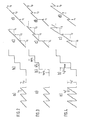
- FIG. 1 shows a block diagram of an embodiment of a digital / analog converter according to the invention
- Figures 2a to d to 4a to d temporal waveforms to explain the embodiment shown in Figure 1.
- 10 denotes a data line on which a digital input signal is present.
- the data line 10 leads to a first n-bit converter 11 and to a second n-bit converter 12.
- the converters 11, 12 have resistance networks R, 2R, 4R, 8R ..., the resistance values of which are graded exponentially.
- the resistors can be switched on by switches, so that a digital / analog conversion of the input signal is possible in this manner known per se.
- the converter 11 is assigned an output resistor R 1
- the converter 12 is assigned an output resistor R 2
- the resistors R1 , R2 lead to a common output 13.
- the step size of the transducers 11, 12 can be set by dimensioning the resistors R 13 R 2 , the step size being understood to mean the rise in the output signal which occurs when the input is supplied with a digital clock signal.
- a staircase-shaped signal is produced at the output 13, as will be described in detail below. which can be converted into a ramp-shaped signal by smoothing measures.
- this ramp-shaped signal is used to control a station search of a car radio 14.
- the signal at output 13 according to the invention can also be used to control other device functions. Since, as also described in detail below, measures according to the invention can be reliably prevented that the ramp function has forward jumps however, the signal at output 13 is particularly well suited for searches, since this ensures that no areas to be covered by the search are skipped. As a result, the voltage at the output 13 can also be used particularly advantageously for measuring purposes, for example in locating devices or analytical measuring devices.
- FIG. 2a shows the output signal of the first converter 11 when a clock signal is applied to it from the data line 10.
- a staircase function that is reset periodically, a step size S 11 being set by dimensioning the resistor R 1 .
- a step-shaped output signal at the output of the second converter 12 is set accordingly to an amount S 12 which corresponds to the total step size of the first converter 11 up to the overflow.
- the time duration of the individual steps of the second converter 12 is adjusted by suitable cycle measures so that each ramp-up to the overflow of the first converter 11 corresponds to one step of the second converter 12.
- both converters 11, 12 are designed as n-bit converters and 2 n steps S 11 of the first converter 11 correspond exactly to one step S 12 of the second converter 12, a staircase voltage is produced by combining the output signals, as is shown in FIG. 2c.
- t, t 2 , t 3 are the times at which the second converter 12 takes over the output signal of the first converter 11, so that the uniform staircase voltage shown in FIG. 2c results overall.
- the course of the voltage in FIG. 2c can now be converted into one according to FIG. 2d. Since the assignments of step number and step size described above ensure a monotonous course of the signal course according to FIG. 2c, the overall result is a strict linear ramp function according to FIG. 2d.
- step size When using simple converters 11, 12 with switched, exponentially stepped resistance networks, however, considerable tolerances can occur in the step size, as is schematically illustrated in FIG. 3b.
- the three steps shown there are 150%, 70% and 100% of the target step size.
- the step size of the first converter 11 according to FIG. 3a is assumed to be constant, a staircase function as shown in FIG. 3c or a smoothed ramp function derived therefrom according to FIG. 3d results. Since the first step is greatly increased in step size by 150%, there is a forward jump in the ramp function according to FIG. 3d at time t 1 .
- the reduced second step size results in a jump back at time t 2 , while at the end of the third jump, which has the target width at 100%, there is a monotonous transition at time t 3 .
- the discontinuities occurring at times t 1 and t 2 can have a disruptive effect when the ramp function according to FIG. 3 is used in a search run if areas to be covered are skipped. This is the case for the forward jump at time t 1 , while the backward jump at time t 2 is only for As a result, a certain area is covered again.
- this second error is not critical, for example, when searching for a station in a car radio, while the first error should be avoided at time t 1 , since this forward jump may mean that important radio stations, for example those that can be skipped by traffic radio.
- the step size S 11 is set by adjusting the resistor R 1 so that an overall increment is calculated up to the overflow of the first transducer 11 of R 12 ', that the maximum expected pitch S 12max corresponds or can be larger. This then results in a staircase function according to FIG. 4c or a smoothed ramp function according to FIG. 4d.
- steps S 11 ' only backward jumps appear at times t 1' t 3 ' while when the maximum step size S 12max of second converter 12 occurs at time t 2, a monotonous transition of the functions according to FIG 4c and d appearance. In this way, it is thus ensured that all areas of the search to be covered are covered and that no more individual areas are skipped.
Landscapes
- Analogue/Digital Conversion (AREA)
- Radar Systems Or Details Thereof (AREA)
- Channel Selection Circuits, Automatic Tuning Circuits (AREA)
Priority Applications (1)
| Application Number | Priority Date | Filing Date | Title |
|---|---|---|---|
| AT82110447T ATE24806T1 (de) | 1982-01-13 | 1982-11-12 | Digital/analog-wandler. |
Applications Claiming Priority (2)
| Application Number | Priority Date | Filing Date | Title |
|---|---|---|---|
| DE19823200748 DE3200748A1 (de) | 1982-01-13 | 1982-01-13 | Digital-analog-wandler |
| DE3200748 | 1982-01-13 |
Publications (2)
| Publication Number | Publication Date |
|---|---|
| EP0083706A1 true EP0083706A1 (fr) | 1983-07-20 |
| EP0083706B1 EP0083706B1 (fr) | 1987-01-07 |
Family
ID=6152946
Family Applications (1)
| Application Number | Title | Priority Date | Filing Date |
|---|---|---|---|
| EP82110447A Expired EP0083706B1 (fr) | 1982-01-13 | 1982-11-12 | Convertisseur numerique-analogique |
Country Status (4)
| Country | Link |
|---|---|
| EP (1) | EP0083706B1 (fr) |
| JP (1) | JPS58123229A (fr) |
| AT (1) | ATE24806T1 (fr) |
| DE (1) | DE3200748A1 (fr) |
Cited By (2)
| Publication number | Priority date | Publication date | Assignee | Title |
|---|---|---|---|---|
| FR2550031A1 (fr) * | 1983-07-28 | 1985-02-01 | Rca Corp | Convertisseur numerique-analogique utile dans un televiseur |
| EP0164748A3 (en) * | 1984-06-13 | 1989-12-13 | Tektronix, Inc. | Method and apparatus for processing an analog signal |
Families Citing this family (2)
| Publication number | Priority date | Publication date | Assignee | Title |
|---|---|---|---|---|
| US4595910A (en) * | 1983-07-28 | 1986-06-17 | Rca Corporation | Digital-to-analog converter useful in a television receiver |
| JP2763273B2 (ja) * | 1995-03-20 | 1998-06-11 | 富士通テン株式会社 | 電子同調ラジオ受信機 |
Citations (5)
| Publication number | Priority date | Publication date | Assignee | Title |
|---|---|---|---|---|
| DE1926077A1 (de) * | 1968-09-27 | 1970-04-02 | Zentrallaboratorium Rundfunk | Schaltungsanordnung zur automatischen Sendersuche |
| FR1593778A (fr) * | 1968-11-28 | 1970-06-01 | ||
| FR2125717A5 (fr) * | 1971-02-18 | 1972-09-29 | Socrat | |
| US3995266A (en) * | 1974-05-17 | 1976-11-30 | Siemens Aktiengesellschaft | Device for setting an electric command variable |
| FR2490429A1 (fr) * | 1980-09-16 | 1982-03-19 | Nippon Telegraph & Telephone | Convertisseur numerique-analogique |
-
1982
- 1982-01-13 DE DE19823200748 patent/DE3200748A1/de not_active Withdrawn
- 1982-11-12 EP EP82110447A patent/EP0083706B1/fr not_active Expired
- 1982-11-12 AT AT82110447T patent/ATE24806T1/de not_active IP Right Cessation
-
1983
- 1983-01-11 JP JP58001810A patent/JPS58123229A/ja active Pending
Patent Citations (5)
| Publication number | Priority date | Publication date | Assignee | Title |
|---|---|---|---|---|
| DE1926077A1 (de) * | 1968-09-27 | 1970-04-02 | Zentrallaboratorium Rundfunk | Schaltungsanordnung zur automatischen Sendersuche |
| FR1593778A (fr) * | 1968-11-28 | 1970-06-01 | ||
| FR2125717A5 (fr) * | 1971-02-18 | 1972-09-29 | Socrat | |
| US3995266A (en) * | 1974-05-17 | 1976-11-30 | Siemens Aktiengesellschaft | Device for setting an electric command variable |
| FR2490429A1 (fr) * | 1980-09-16 | 1982-03-19 | Nippon Telegraph & Telephone | Convertisseur numerique-analogique |
Cited By (2)
| Publication number | Priority date | Publication date | Assignee | Title |
|---|---|---|---|---|
| FR2550031A1 (fr) * | 1983-07-28 | 1985-02-01 | Rca Corp | Convertisseur numerique-analogique utile dans un televiseur |
| EP0164748A3 (en) * | 1984-06-13 | 1989-12-13 | Tektronix, Inc. | Method and apparatus for processing an analog signal |
Also Published As
| Publication number | Publication date |
|---|---|
| ATE24806T1 (de) | 1987-01-15 |
| JPS58123229A (ja) | 1983-07-22 |
| EP0083706B1 (fr) | 1987-01-07 |
| DE3200748A1 (de) | 1983-07-21 |
Similar Documents
| Publication | Publication Date | Title |
|---|---|---|
| DE3902313C3 (de) | Analog /Digitalwandler | |
| DE2622956C2 (de) | Elektrische Schaltung zum Melden der Kanalwahl bei einem abstimmbaren Empfänger | |
| DE3003099C2 (de) | Digital-Analog-Wandler mit Kompensationsschaltung | |
| DE69015373T2 (de) | Digital-analog-wandler mit grossem dynamikbereich, hoher genauigkeit und hoher geschwindigkeit. | |
| DE3879250T2 (de) | Ansteuerungsvorrichtung fuer einen halbleiterlaser. | |
| DE3715237A1 (de) | Mit bereichsteilung arbeitender analog/digital-wandler | |
| DE2333299C3 (de) | Schaltungsanordnung zur Umsetzung von Analog-Signalen in PCM-Signale und von PCM-Signalen in Analog-Signale | |
| DE3149494C2 (fr) | ||
| EP0472555B1 (fr) | Convertisseur numerique-analogique a haute linearite | |
| DE3427852C2 (fr) | ||
| DE2201939C3 (de) | A-Codierer mit automatischem Ladungsabgleich | |
| EP0083706A1 (fr) | Convertisseur numerique-analogique | |
| DE2704756C2 (de) | Digital-Analog-Umsetzer | |
| DE2632025A1 (de) | Abstimmschaltung fuer hochfrequenzempfangsgeraete nach dem ueberlagerungsprinzip | |
| DE2821240C2 (de) | Optoelektronische Abtasteinrichtung | |
| DE2740833C2 (de) | Schaltungsanordnung zum Betreiben elektromechanischer Schaltwerke | |
| DE2424930C3 (de) | Anordnung zur Analog/Digitalumwandlung | |
| DE2337132A1 (de) | Dezimale grenzwerteinstellung zum vergleich mit einem binaeren digitalsignal | |
| DE2606230C3 (de) | Abstimmschaltung für Überlagerungsempfänger | |
| DE1142385B (de) | Anordnung zur nichtlinearen Codierung und Decodierung | |
| DE4106431C1 (fr) | ||
| DE2627206C3 (de) | Schaltung zur Erzeugung von Pulsfolgen | |
| DE2319986C3 (de) | Digital-Analog-Umsetzer | |
| DE3037021C2 (fr) | ||
| DE2848943C2 (de) | Anordnung zum stochastischen Kodieren von mindestens zwei Größen |
Legal Events
| Date | Code | Title | Description |
|---|---|---|---|
| PUAI | Public reference made under article 153(3) epc to a published international application that has entered the european phase |
Free format text: ORIGINAL CODE: 0009012 |
|
| AK | Designated contracting states |
Designated state(s): AT FR IT |
|
| 17P | Request for examination filed |
Effective date: 19831223 |
|
| GRAA | (expected) grant |
Free format text: ORIGINAL CODE: 0009210 |
|
| AK | Designated contracting states |
Kind code of ref document: B1 Designated state(s): AT FR IT |
|
| REF | Corresponds to: |
Ref document number: 24806 Country of ref document: AT Date of ref document: 19870115 Kind code of ref document: T |
|
| ET | Fr: translation filed | ||
| ITF | It: translation for a ep patent filed | ||
| PLBE | No opposition filed within time limit |
Free format text: ORIGINAL CODE: 0009261 |
|
| STAA | Information on the status of an ep patent application or granted ep patent |
Free format text: STATUS: NO OPPOSITION FILED WITHIN TIME LIMIT |
|
| 26N | No opposition filed | ||
| PG25 | Lapsed in a contracting state [announced via postgrant information from national office to epo] |
Ref country code: AT Effective date: 19881112 |
|
| PG25 | Lapsed in a contracting state [announced via postgrant information from national office to epo] |
Ref country code: FR Free format text: LAPSE BECAUSE OF NON-PAYMENT OF DUE FEES Effective date: 19890731 |
|
| REG | Reference to a national code |
Ref country code: FR Ref legal event code: ST |